US8208883B2 - Receiver with low power consumption - Google Patents
Receiver with low power consumption Download PDFInfo
- Publication number
- US8208883B2 US8208883B2 US12/369,948 US36994809A US8208883B2 US 8208883 B2 US8208883 B2 US 8208883B2 US 36994809 A US36994809 A US 36994809A US 8208883 B2 US8208883 B2 US 8208883B2
- Authority
- US
- United States
- Prior art keywords
- gain
- amplifier
- programmable
- bandwidth product
- intermediate frequency
- Prior art date
- Legal status (The legal status is an assumption and is not a legal conclusion. Google has not performed a legal analysis and makes no representation as to the accuracy of the status listed.)
- Expired - Fee Related, expires
Links
- 238000013507 mapping Methods 0.000 claims description 13
- 230000003247 decreasing effect Effects 0.000 abstract description 4
- 238000010586 diagram Methods 0.000 description 6
- 239000003990 capacitor Substances 0.000 description 4
- 238000004891 communication Methods 0.000 description 4
- 238000013461 design Methods 0.000 description 2
- 238000012986 modification Methods 0.000 description 2
- 230000004048 modification Effects 0.000 description 2
- 238000012546 transfer Methods 0.000 description 2
- 230000006835 compression Effects 0.000 description 1
- 238000007906 compression Methods 0.000 description 1
- 230000007423 decrease Effects 0.000 description 1
Images


Classifications
-
- H—ELECTRICITY
- H04—ELECTRIC COMMUNICATION TECHNIQUE
- H04B—TRANSMISSION
- H04B1/00—Details of transmission systems, not covered by a single one of groups H04B3/00 - H04B13/00; Details of transmission systems not characterised by the medium used for transmission
- H04B1/06—Receivers
-
- H—ELECTRICITY
- H03—ELECTRONIC CIRCUITRY
- H03G—CONTROL OF AMPLIFICATION
- H03G3/00—Gain control in amplifiers or frequency changers
- H03G3/20—Automatic control
- H03G3/30—Automatic control in amplifiers having semiconductor devices
- H03G3/3052—Automatic control in amplifiers having semiconductor devices in bandpass amplifiers (H.F. or I.F.) or in frequency-changers used in a (super)heterodyne receiver
- H03G3/3068—Circuits generating control signals for both R.F. and I.F. stages
Definitions
- the present invention relates to a receiver in a communication system, and more particularly to a receiver with low power consumption, wherein the receiver with low power consumption controls the gain of a programmable gain amplifier (PGA) based on the automatic gain control, and a current-adjusting unit optimizes the gain bandwidth for adjusting the current provided for the programmable gain amplifier (PGA) in order to minimize the power consumption of the receiver.
- PGA programmable gain amplifier
- FIG. 1 it is a schematic block diagram of a conventional receiver 100 with a programmable gain amplifier 105 .
- the receiver 100 includes an antenna 101 , a low noise amplifier (LNA) 102 , a frequency converter 103 , a channel selection filter (CSF) 104 and a programmable gain amplifier (PGA) 105 .
- LNA low noise amplifier
- CSF channel selection filter
- PGA programmable gain amplifier
- the receiver 100 receives the ultra-high signal by the antenna 101 and the low noise amplifier (LNA) 102 amplifies the received signal.
- the frequency converter 103 down-converts the frequency of the received signal.
- the channel selection filter (CSF) 104 filters away the interference signal of the received signal.
- the programmable gain amplifier (PGA) 105 composed of amplifiers amplifies the received signal and outputs a signal at a predetermined value.
- the receiver 100 further includes a radio frequency automatic gain control (RF AGC) 107 and an intermediate frequency automatic gain control (IF AGC) 108 .
- the radio frequency automatic gain control (RF AGC) 107 automatically adjusts the gain of the low noise amplifier (LNA) 102 and the frequency converter 103 to maintain the ultra-high signal before being inputted to the channel selection filter (CSF) 104 at a predetermined value.
- the intermediate frequency automatic gain control (IF AGC) 108 automatically adjusts the gain of the channel selection filter (CSF) 104 and the programmable gain amplifier (PGA) 105 to maintain the signal after being outputted from the channel selection filter (CSF) 104 at a predetermined value.
- the programmable gain amplifier (PGA) 105 While the signal inputted to the programmable gain amplifier (PGA) 105 is too low, the programmable gain amplifier (PGA) 105 increases the gain for the signal under the control of the intermediate frequency automatic gain control (IF AGC) 108 . While the signal inputted to the programmable gain amplifier (PGA) 105 is too high, the programmable gain amplifier (PGA) 105 decreases the gain for the signal to maintain the signal at the predetermined value.
- IF AGC intermediate frequency automatic gain control
- FIG. 2 It is a schematic view of a conventional programmable gain amplifier (PGA) 105 implemented by operational amplifiers.
- the programmable gain amplifier (PGA) 105 includes a first operational amplifier 201 , a second amplifier 202 , and a plurality of resistors R 201 , R 202 , and R 203 .
- the transfer function of the programmable gain amplifier (PGA) 105 is represented as formula 1 (E1):
- V o V i R 202 ⁇ R 204 R 201 ⁇ R 203 ( E1 )
- Vo Vop ⁇ Vom
- Vi Vip ⁇ Vim
- the programmable gain amplifier (PGA) 105 performs mapping for the gain which is inversely proportional to the input signal in the communication system.
- the high level signal is corresponding to low gain
- low level signal is corresponding to high gain so that the outputted signal is maintained at the predetermined value.
- the frequency bandwidth, noise characteristic, 1 dB output gain compression point, and 3 rd output intercept point (OIP 3 ) meet the specification requirement of the communication system.
- FIG. 5 It is a schematic view of the relationship between the gain and frequency bandwidth of the conventional programmable gain amplifier (PGA) 105 .
- the relationship between the gain and frequency bandwidth (BW) of the programmable gain amplifier (PGA) 105 is represented as formula 2 (E2), and the gain is inversely proportional to the frequency bandwidth (BW):
- the frequency bandwidth (BW) is decreased when the gain of the programmable gain amplifier 105 is increased.
- the programmable gain amplifier (PGA) 105 is constructed as the following design rule. In the worst case, the programmable gain amplifier (PGA) 105 is designed on the basis of the high gain rule first, and the gain bandwidth product is then determined.
- the greater current is provided to the operational amplifiers thereby the programmable gain amplifier (PGA) 105 is operated in the status of high gain. Even though the programmable gain amplifier (PGA) 105 is only required to be operated in the status of low gain, or the outputted signal of the programmable gain amplifier (PGA) 105 is maintained at the predetermined value, the greater current is always provided to the operational amplifiers, thereby resulting in excessive power consumption with respect to the receiver 100 .
- the programmable gain amplifier (PGA) 105 has to be operated in high gain in only a few cases that the inputted signal is in very low level, it is necessary to provide the greater current for the programmable gain amplifier (PGA) 105 all the time.
- the gain of the programmable gain amplifier (PGA) 105 is designed by a gain margin so that the greater current is provided for the programmable gain amplifier (PGA) 105 all the time. Therefore, it is required to supply more current to the programmable gain amplifier (PGA) 105 , thereby resulting in a problem of unnecessary power consumption.
- the first objective of the present invention is to provide a receiver with low power consumption.
- the receiver with low power consumption controls the gain of a programmable gain amplifier (PGA) based on the automatic gain control.
- a current-adjusting unit optimizes the gain bandwidth product for adjusting the current exerted on the first stage amplifier of at least two stage amplifiers in the programmable gain amplifier (PGA) based on the gain bandwidth product in order to minimize the power consumption of the receiver due to undue current.
- the present invention sets forth a receiver with low power consumption.
- the receiver includes an antenna, a low noise amplifier (LNA), a frequency converter, a channel selection filter (CSF), a programmable gain amplifier (PGA), a radio frequency automatic gain control (RF AGC), and an intermediate frequency automatic gain control (IF AGC).
- the low noise amplifier (LNA) amplifies an ultra-high frequency signal received from the antenna.
- the frequency converter down-converts a frequency of the ultra-high frequency signal.
- the channel selection filter (CSF) filters away an interference signal from the down-converted signal from the channel selection filter.
- the programmable gain amplifier (PGA) amplifies the down-converted signal for outputting a gain-amplified signal having a predetermined constant value to the output end.
- the intermediate frequency automatic gain control (IF AGC) generates intermediate frequency automatic gain control information based on an inputted signal of the programmable gain amplifier to adjust the gain of the programmable gain amplifier (PGA).
- the receiver further includes a current-adjusting unit.
- the current-adjusting unit is coupled to the intermediate frequency automatic gain control (IF AGC) and the programmable gain amplifier (PGA).
- the current-adjusting unit receives the intermediate frequency automatic gain control information and determines an optimal gain bandwidth product of the programmable gain amplifier according to the intermediate frequency automatic gain control information.
- the current-adjusting unit further adjusts the current of the programmable gain amplifier (PGA) based on the optimal gain bandwidth product, wherein the optimal gain bandwidth product includes a first gain bandwidth product and a second gain bandwidth product which is less than the first gain bandwidth product.
- FIG. 1 is a schematic block diagram of a conventional receiver with a programmable gain amplifier
- FIG. 2 is a schematic view of a conventional programmable gain amplifier implemented by operational amplifiers
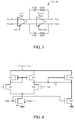
- FIG. 3 is a schematic view of a two-stage operational amplifier of a programmable gain amplifier according to one embodiment of the present invention
- FIG. 4 is a schematic circuit view of the two-stage operational amplifier according to one embodiment of the present invention.
- FIG. 5 is a schematic view of the relationship between the gain and frequency bandwidth of the conventional programmable gain amplifier
- FIG. 6 is a schematic block diagram of a receiver with a current-adjusting unit according to one embodiment of the present invention.
- FIG. 7 is a schematic view diagram of the current-adjusting unit according to one embodiment of the present invention.
- FIG. 6 It is a schematic block diagram of a receiver 600 with a current-adjusting unit for reducing power consumption by optimizing the gain bandwidth product according to one embodiment of the present invention.
- the receiver 600 includes an antenna 601 , a low noise amplifier (LNA) 602 , a frequency converter 603 , a channel selection filter (CSF) 604 , a programmable gain amplifier (PGA) 605 , a radio frequency automatic gain control (RF AGC) 607 , and an intermediate frequency automatic gain control (IF AGC) 608 .
- the low noise amplifier (LNA) 602 amplifies an ultra-high frequency signal received from the antenna 601 .
- the frequency converter 603 down-converts a frequency of the ultra-high frequency signal.
- the channel selection filter (CSF) 604 filters away an interference signal from the down-converted signal.
- the programmable gain amplifier (PGA) 605 amplifies the down-converted signal from channel selection filter (CSF) 604 for outputting a gain-amplified signal having a predetermined constant value to the output end 606 .
- the intermediate frequency automatic gain control (IF AGC) 608 generates intermediate frequency automatic gain control information based on an inputted signal of the programmable gain amplifier (PGA) 605 to adjust the gain of the programmable gain amplifier (PGA) 605 .
- the receiver 600 further includes a current-adjusting unit 700 .
- the current-adjusting unit 700 is coupled to the intermediate frequency automatic gain control (IF AGC) 608 and the programmable gain amplifier (PGA) 605 .
- the current-adjusting unit 700 receives the intermediate frequency automatic gain control information and determines an optimal gain bandwidth product of the programmable gain amplifier according to the intermediate frequency automatic gain control information.
- the current-adjusting unit 700 further adjusts the current of the programmable gain amplifier (PGA) 605 based on the optimal gain bandwidth product, wherein the optimal gain bandwidth product includes a first gain bandwidth product and a second gain bandwidth product which is less than the first gain bandwidth product.
- PGA programmable gain amplifier
- FIG. 7 is a schematic view diagram of the current-adjusting unit 700 according to one embodiment of the present invention.
- the current-adjusting unit 700 further includes an information-receiving module 710 for intermediate frequency automatic gain control, a gain bandwidth product mapping module 720 , and a reference current control module 730 .
- the information-receiving module 710 for intermediate frequency automatic gain control is coupled to the intermediate frequency automatic gain control 608 and receives the intermediate frequency automatic gain control information.
- the intermediate frequency automatic gain control information is a gain control signal which is adjusted according to the inputted signal of the programmable gain amplifier (PGA) 605 .
- the gain bandwidth product mapping module 720 determines the optimal gain bandwidth product based on the intermediate frequency automatic gain control information.
- the reference current control module 730 generates a reference current which is corresponding to the optimal gain bandwidth product and supplies the reference current to the programmable gain amplifier (PGA) 605 .
- FIG. 3 is a schematic view of a two-stage operational amplifier of the programmable gain amplifier (PGA) 605 according to one embodiment of the present invention.
- FIG. 2 is one embodiment in FIG. 3 of the present invention.
- the programmable gain amplifier (PGA) 605 includes a first operational amplifier 201 and a second operational amplifier 202 , which are a two-stage amplifier.
- the two-stage amplifier includes a loop circuit comprising capacitors C 301 and resistors R 301 and has input signals (Vip, Vim). The input signals (Vip, Vim) are directly inputted to the first stage circuit.
- the loop circuit composed of capacitors C 301 and resistors R 301 outputs the signal (Vip, Vim) from the second stage circuit.
- the first reference current (iref 1 ) is exerted on the first stage circuit
- the second reference current (iref 2 ) is exerted on the second stage circuit.
- FIG. 4 is a schematic view of the circuit of the two-stage operational amplifier according to one embodiment of the present invention.
- FIG. 4 is one embodiment in FIG. 3 of the present invention.
- the two-stage amplifier from the first transistor “M 1 ” to fifth transistor “M 5 ” (i.e. “M 1 ”, “M 2 ”, “M 3 ”, “M 4 ”, and “M 5 ”) constructs a current mirror.
- the two-stage amplifier further includes a sixth transistor “M 6 ” and seventh transistor “M 7 ”.
- the common electrode of the first transistor “M 1 ” and the second transistor “M 2 ” is connected to one electrode of the transistor “M 5 ”, wherein the gate of transistor “M 5 ” is controlled by the voltage “Vbias”. Additionally, another electrode of the transistor “M 2 ” is connected to the gate of the transistor “M 6 ”. A capacitor “C c ” is positioned between the gate and one electrode of the transistor “M 6 ”. That is, one electrode of capacitor “C c ” is connected to one electrode of transistor “M 6 ”. The voltage “Vbias” is applied to the gate of transistor “M 7 ”.
- the gain of the two-stage amplifier is proportional to the transconductance “g m ” of the transistor “M 1 ”.
- the transconductance g m of the transistor “M 1 ” is proportional to the square root of current “I” of transistor “M 5 ”.
- the transfer function of the programmable gain amplifier (PGA) 605 is represented by a plurality of resistors, which is uncorrelated with the gain of the operational amplifier. Therefore, while the supplied current is reduced by the present invention, the performance of the programmable gain amplifier (PGA) 605 is kept in a better mode all the time.
- the programmable gain amplifier (PGA) 605 utilizes the intermediate frequency automatic gain control information to control the gain for determining the reference current of the optimal gain bandwidth product.
- the reference current control module 730 provides the reference current to a first stage amplifier of a two-stage amplifier in the programmable gain amplifier (PGA) 605 .
- the information-receiving module 710 for the intermediate frequency automatic gain control receives the intermediate frequency automatic gain control information.
- the intermediate frequency automatic gain control information is the gain value of the programmable gain amplifier (PGA) 605 .
- the gain value can be adjusted by the intermediate frequency automatic gain control (IF AGC) 608 according to the inputted signal of the programmable gain amplifier (PGA) 605 . In other words, when the inputted signal of the programmable gain amplifier (PGA) 605 is in low level, the gain value of the programmable gain amplifier (PGA) 605 is increased. When the inputted signal of the programmable gain amplifier (PGA) 605 is in high level, the gain value of the programmable gain amplifier (PGA) 605 is decreased.
- IF AGC intermediate frequency automatic gain control
- the gain value of the programmable gain amplifier (PGA) 605 is constant, and the programmable gain amplifier (PGA) 605 is operated according to the constant gain value while the intermediate frequency automatic gain control (IF AGC) 608 is in an idle status. Therefore, based on the statuses of the inputted and outputted signals, the intermediate frequency automatic gain control information, e.g. the high gain, the low gain, or the constant gain, is received.
- the intermediate frequency automatic gain control information e.g. the high gain, the low gain, or the constant gain
- the gain bandwidth product mapping module 720 determines the optimal gain bandwidth product by mapping the gain used in the programmable gain amplifier (PGA) 605 . While the programmable gain amplifier (PGA) 605 is in a status of high gain based on the intermediate frequency automatic gain control information, the gain bandwidth product mapping module 720 maps out the first gain bandwidth product, and the reference current control module 730 provides a high current, serving as the reference current, to the programmable gain amplifier (PGA) 605 based on the first gain bandwidth.
- the gain bandwidth product mapping module 720 maps out the second gain bandwidth
- the reference current control module 730 provides a low current, serving as the reference current, to the programmable gain amplifier (PGA) 605 based on the second gain bandwidth. Since the mapping between the gain and the frequency bandwidth is performed in the present invention, the reduced (smaller) gain bandwidth product can satisfy the requirement of predetermined bandwidth (BW).
- the reference current control module 730 controls the reference current of the first stage circuit in the two-stage amplifier.
- the reference current control module 730 provides a higher current, serving as the reference current, to the first stage circuit of the programmable gain amplifier (PGA) 605 based on the first gain bandwidth product.
- the higher current is computed by gain and bandwidth, i.e. the reference current can satisfy the requirement of the gain bandwidth product.
- the reference current control module 730 provides a lower current, serving as the reference current, to the first stage circuit of the programmable gain amplifier (PGA) 605 based on the second gain bandwidth product.
- the receiver with low power consumption controls the gain of a programmable gain amplifier (PGA) 605 based on the input signal of the programmable gain amplifier (PGA) 605 to determine the gain bandwidth product.
- the determined gain bandwidth product is implemented by adjusting the reference current exerted on the first stage amplifier of at least two stage amplifiers in the programmable gain amplifier (PGA) 605 . Therefore, a sufficient gain bandwidth product can be applied according to different gains, and minimizing the power consumption of the receiver due to undue current.
Landscapes
- Engineering & Computer Science (AREA)
- Computer Networks & Wireless Communication (AREA)
- Signal Processing (AREA)
- Circuits Of Receivers In General (AREA)
- Control Of Amplification And Gain Control (AREA)
- Superheterodyne Receivers (AREA)
- Input Circuits Of Receivers And Coupling Of Receivers And Audio Equipment (AREA)
Abstract
Description
Claims (4)
Applications Claiming Priority (2)
| Application Number | Priority Date | Filing Date | Title |
|---|---|---|---|
| KR1020080013267A KR100966767B1 (en) | 2008-02-14 | 2008-02-14 | 수신기 Receiver with current regulator to reduce power consumption through optimization |
| KR10-2008-0013267 | 2008-02-14 |
Publications (2)
| Publication Number | Publication Date |
|---|---|
| US20090209221A1 US20090209221A1 (en) | 2009-08-20 |
| US8208883B2 true US8208883B2 (en) | 2012-06-26 |
Family
ID=40955588
Family Applications (1)
| Application Number | Title | Priority Date | Filing Date |
|---|---|---|---|
| US12/369,948 Expired - Fee Related US8208883B2 (en) | 2008-02-14 | 2009-02-12 | Receiver with low power consumption |
Country Status (4)
| Country | Link |
|---|---|
| US (1) | US8208883B2 (en) |
| KR (1) | KR100966767B1 (en) |
| CN (1) | CN101510786B (en) |
| TW (1) | TWI388131B (en) |
Cited By (1)
| Publication number | Priority date | Publication date | Assignee | Title |
|---|---|---|---|---|
| US12074577B2 (en) | 2022-06-27 | 2024-08-27 | Renesas Design Technology Inc. | Active filter |
Families Citing this family (6)
| Publication number | Priority date | Publication date | Assignee | Title |
|---|---|---|---|---|
| JP2014107730A (en) * | 2012-11-28 | 2014-06-09 | Yamaha Corp | Signal processing device and amplifier |
| CN104253591B (en) * | 2013-06-28 | 2017-10-17 | 成都振芯科技股份有限公司 | Suitable for the automatic controlling method for gain of big input dynamic range |
| CN104579390B (en) * | 2014-02-17 | 2017-07-07 | 上海奎信微电子技术有限公司 | ASK wireless receivers and its auto gain control method |
| CN107994878B (en) * | 2017-11-28 | 2021-10-29 | 中科亿海微电子科技(苏州)有限公司 | Low-noise amplifier for analog bus receiver and analog bus receiver |
| US11570709B2 (en) * | 2019-01-14 | 2023-01-31 | The Regents Of The University Of California | BLE and/or WiFi compliant and blocker-resilient wake-up receiver and method |
| CN113904694A (en) * | 2021-10-29 | 2022-01-07 | 上海力通通信有限公司 | Gain control circuit, device and radio frequency signal processing system |
Citations (12)
| Publication number | Priority date | Publication date | Assignee | Title |
|---|---|---|---|---|
| US6278325B1 (en) * | 2000-12-13 | 2001-08-21 | Industrial Technology Research Institute | Programmable gain amplifier with a large extent for the variation of gains |
| US20030181179A1 (en) * | 2002-03-25 | 2003-09-25 | Hooman Darabi | Analog power detection for gain control operations |
| US6683925B1 (en) * | 1999-02-24 | 2004-01-27 | Mitsubishi Denki Kabushiki Kaisha | Wireless terminal device |
| US20040061554A1 (en) * | 2002-09-26 | 2004-04-01 | Hitachi, Ltd. | Variable gain amplifier for use in communications |
| CN1529947A (en) | 2001-07-27 | 2004-09-15 | ���µ�����ҵ��ʽ���� | receivers and communication terminals |
| US20050107054A1 (en) * | 2003-09-16 | 2005-05-19 | Sony Ericsson Mobile Communications Japan, Inc. | Variable gain control circuit and receiver apparatus using the circuit |
| US6968166B2 (en) * | 2002-01-22 | 2005-11-22 | George L. Yang | Method and apparatus of a fast digital automatic gain control circuit |
| US6993291B2 (en) * | 2001-10-11 | 2006-01-31 | Nokia Corporation | Method and apparatus for continuously controlling the dynamic range from an analog-to-digital converter |
| US20070026837A1 (en) * | 2005-07-29 | 2007-02-01 | Broadcom Corporation, A California Corporation | MIMO radio interfaces |
| US7292101B2 (en) * | 2005-04-27 | 2007-11-06 | Broadcom Corporation | Digitally adjustable variable gain amplifier (VGA) using switchable differential pairs |
| US7469134B2 (en) * | 2003-12-01 | 2008-12-23 | Sony Ericsson Mobile Communications Japan, Inc. | Mobile communication terminal apparatus, a variable gain amplifier circuit and a gain control circuit |
| US7676206B2 (en) * | 2005-12-05 | 2010-03-09 | Sigmatel, Inc. | Low noise, low distortion radio receiver front-end |
Family Cites Families (1)
| Publication number | Priority date | Publication date | Assignee | Title |
|---|---|---|---|---|
| US5722061A (en) | 1994-12-16 | 1998-02-24 | Qualcomm Incorporated | Method and apparatus for increasing receiver immunity to interference |
-
2008
- 2008-02-14 KR KR1020080013267A patent/KR100966767B1/en not_active Expired - Fee Related
- 2008-12-16 CN CN2008101884733A patent/CN101510786B/en not_active Expired - Fee Related
-
2009
- 2009-01-07 TW TW098100373A patent/TWI388131B/en not_active IP Right Cessation
- 2009-02-12 US US12/369,948 patent/US8208883B2/en not_active Expired - Fee Related
Patent Citations (13)
| Publication number | Priority date | Publication date | Assignee | Title |
|---|---|---|---|---|
| US6683925B1 (en) * | 1999-02-24 | 2004-01-27 | Mitsubishi Denki Kabushiki Kaisha | Wireless terminal device |
| US6278325B1 (en) * | 2000-12-13 | 2001-08-21 | Industrial Technology Research Institute | Programmable gain amplifier with a large extent for the variation of gains |
| CN1529947A (en) | 2001-07-27 | 2004-09-15 | ���µ�����ҵ��ʽ���� | receivers and communication terminals |
| US20040218576A1 (en) | 2001-07-27 | 2004-11-04 | Yasumi Imagawa | Receiver and communication terminal |
| US6993291B2 (en) * | 2001-10-11 | 2006-01-31 | Nokia Corporation | Method and apparatus for continuously controlling the dynamic range from an analog-to-digital converter |
| US6968166B2 (en) * | 2002-01-22 | 2005-11-22 | George L. Yang | Method and apparatus of a fast digital automatic gain control circuit |
| US20030181179A1 (en) * | 2002-03-25 | 2003-09-25 | Hooman Darabi | Analog power detection for gain control operations |
| US20040061554A1 (en) * | 2002-09-26 | 2004-04-01 | Hitachi, Ltd. | Variable gain amplifier for use in communications |
| US20050107054A1 (en) * | 2003-09-16 | 2005-05-19 | Sony Ericsson Mobile Communications Japan, Inc. | Variable gain control circuit and receiver apparatus using the circuit |
| US7469134B2 (en) * | 2003-12-01 | 2008-12-23 | Sony Ericsson Mobile Communications Japan, Inc. | Mobile communication terminal apparatus, a variable gain amplifier circuit and a gain control circuit |
| US7292101B2 (en) * | 2005-04-27 | 2007-11-06 | Broadcom Corporation | Digitally adjustable variable gain amplifier (VGA) using switchable differential pairs |
| US20070026837A1 (en) * | 2005-07-29 | 2007-02-01 | Broadcom Corporation, A California Corporation | MIMO radio interfaces |
| US7676206B2 (en) * | 2005-12-05 | 2010-03-09 | Sigmatel, Inc. | Low noise, low distortion radio receiver front-end |
Cited By (1)
| Publication number | Priority date | Publication date | Assignee | Title |
|---|---|---|---|---|
| US12074577B2 (en) | 2022-06-27 | 2024-08-27 | Renesas Design Technology Inc. | Active filter |
Also Published As
| Publication number | Publication date |
|---|---|
| TWI388131B (en) | 2013-03-01 |
| CN101510786B (en) | 2013-01-23 |
| KR20090087990A (en) | 2009-08-19 |
| KR100966767B1 (en) | 2010-06-29 |
| US20090209221A1 (en) | 2009-08-20 |
| CN101510786A (en) | 2009-08-19 |
| TW200935768A (en) | 2009-08-16 |
Similar Documents
| Publication | Publication Date | Title |
|---|---|---|
| US8208883B2 (en) | Receiver with low power consumption | |
| US7427897B2 (en) | Power amplifier with close-loop adaptive voltage supply | |
| US7800450B2 (en) | Re-configurable low noise amplifier utilizing feedback capacitors | |
| US6885246B2 (en) | High frequency amplifier | |
| US8260225B2 (en) | Power amplifier controller circuit | |
| US20090021303A1 (en) | Distortion-Driven Power Amplifier Power Supply Controller | |
| US6690237B2 (en) | High frequency power amplifier, and communication apparatus | |
| US8653891B2 (en) | Collector boost | |
| US20100194476A1 (en) | Amplifier compression adjustment circuit | |
| US8525595B2 (en) | Vramp limiting using resistors | |
| US7265627B2 (en) | Self adaptable bias circuit for enabling dynamic control of quiescent current in a linear power amplifier | |
| US9705536B2 (en) | Tunable balun | |
| US7548116B2 (en) | High-frequency circuit of reduced circuit scale | |
| US10367466B2 (en) | Hybrid variable gain amplifier | |
| US12244269B2 (en) | Power amplifier | |
| JP3854832B2 (en) | High frequency power amplifier and communication terminal | |
| US7706761B2 (en) | Power amplifying circuit in mobile terminal | |
| US7250817B2 (en) | Linear power efficient radio frequency (RF) driver system and method with power level control | |
| KR20000018301A (en) | Device and a method thereof for receiving efficiency and a high dynamic range in a mobile communications terminal device | |
| JP2006020035A (en) | Wireless communication device | |
| JP2000216652A (en) | Automatic gain control amplifier |
Legal Events
| Date | Code | Title | Description |
|---|---|---|---|
| AS | Assignment |
Owner name: SILICON MOTION, INC., TAIWAN Free format text: ASSIGNMENT OF ASSIGNORS INTEREST;ASSIGNORS:JEONG, SEONG-HEON;BECK, SUNG-HO;HWANG, MYUNG-WOON;REEL/FRAME:022249/0822 Effective date: 20081027 |
|
| ZAAA | Notice of allowance and fees due |
Free format text: ORIGINAL CODE: NOA |
|
| ZAAB | Notice of allowance mailed |
Free format text: ORIGINAL CODE: MN/=. |
|
| STCF | Information on status: patent grant |
Free format text: PATENTED CASE |
|
| FPAY | Fee payment |
Year of fee payment: 4 |
|
| AS | Assignment |
Owner name: FCI INC., KOREA, REPUBLIC OF Free format text: ASSIGNMENT OF ASSIGNORS INTEREST;ASSIGNOR:SILICON MOTION, INC.;REEL/FRAME:049163/0626 Effective date: 20181231 |
|
| FEPP | Fee payment procedure |
Free format text: ENTITY STATUS SET TO SMALL (ORIGINAL EVENT CODE: SMAL); ENTITY STATUS OF PATENT OWNER: SMALL ENTITY |
|
| MAFP | Maintenance fee payment |
Free format text: PAYMENT OF MAINTENANCE FEE, 8TH YR, SMALL ENTITY (ORIGINAL EVENT CODE: M2552); ENTITY STATUS OF PATENT OWNER: SMALL ENTITY Year of fee payment: 8 |
|
| AS | Assignment |
Owner name: DIALOG SEMICONDUCTOR KOREA INC., KOREA, REPUBLIC OF Free format text: ASSIGNMENT OF ASSIGNORS INTEREST;ASSIGNOR:FCI INC.;REEL/FRAME:053702/0013 Effective date: 20200728 |
|
| FEPP | Fee payment procedure |
Free format text: MAINTENANCE FEE REMINDER MAILED (ORIGINAL EVENT CODE: REM.); ENTITY STATUS OF PATENT OWNER: SMALL ENTITY |
|
| LAPS | Lapse for failure to pay maintenance fees |
Free format text: PATENT EXPIRED FOR FAILURE TO PAY MAINTENANCE FEES (ORIGINAL EVENT CODE: EXP.); ENTITY STATUS OF PATENT OWNER: SMALL ENTITY |
|
| STCH | Information on status: patent discontinuation |
Free format text: PATENT EXPIRED DUE TO NONPAYMENT OF MAINTENANCE FEES UNDER 37 CFR 1.362 |
|
| FP | Lapsed due to failure to pay maintenance fee |
Effective date: 20240626 |