US8206023B2 - Backlight assembly and display device having the same - Google Patents
Backlight assembly and display device having the same Download PDFInfo
- Publication number
- US8206023B2 US8206023B2 US12/584,520 US58452009A US8206023B2 US 8206023 B2 US8206023 B2 US 8206023B2 US 58452009 A US58452009 A US 58452009A US 8206023 B2 US8206023 B2 US 8206023B2
- Authority
- US
- United States
- Prior art keywords
- lamp
- generating unit
- light generating
- wire
- backlight assembly
- Prior art date
- Legal status (The legal status is an assumption and is not a legal conclusion. Google has not performed a legal analysis and makes no representation as to the accuracy of the status listed.)
- Expired - Fee Related, expires
Links
Images


Classifications
-
- G—PHYSICS
- G02—OPTICS
- G02B—OPTICAL ELEMENTS, SYSTEMS OR APPARATUS
- G02B6/00—Light guides; Structural details of arrangements comprising light guides and other optical elements, e.g. couplings
- G02B6/0001—Light guides; Structural details of arrangements comprising light guides and other optical elements, e.g. couplings specially adapted for lighting devices or systems
- G02B6/0011—Light guides; Structural details of arrangements comprising light guides and other optical elements, e.g. couplings specially adapted for lighting devices or systems the light guides being planar or of plate-like form
- G02B6/0081—Mechanical or electrical aspects of the light guide and light source in the lighting device peculiar to the adaptation to planar light guides, e.g. concerning packaging
- G02B6/0086—Positioning aspects
- G02B6/009—Positioning aspects of the light source in the package
-
- G—PHYSICS
- G02—OPTICS
- G02F—OPTICAL DEVICES OR ARRANGEMENTS FOR THE CONTROL OF LIGHT BY MODIFICATION OF THE OPTICAL PROPERTIES OF THE MEDIA OF THE ELEMENTS INVOLVED THEREIN; NON-LINEAR OPTICS; FREQUENCY-CHANGING OF LIGHT; OPTICAL LOGIC ELEMENTS; OPTICAL ANALOGUE/DIGITAL CONVERTERS
- G02F1/00—Devices or arrangements for the control of the intensity, colour, phase, polarisation or direction of light arriving from an independent light source, e.g. switching, gating or modulating; Non-linear optics
- G02F1/01—Devices or arrangements for the control of the intensity, colour, phase, polarisation or direction of light arriving from an independent light source, e.g. switching, gating or modulating; Non-linear optics for the control of the intensity, phase, polarisation or colour
- G02F1/13—Devices or arrangements for the control of the intensity, colour, phase, polarisation or direction of light arriving from an independent light source, e.g. switching, gating or modulating; Non-linear optics for the control of the intensity, phase, polarisation or colour based on liquid crystals, e.g. single liquid crystal display cells
- G02F1/133—Constructional arrangements; Operation of liquid crystal cells; Circuit arrangements
- G02F1/1333—Constructional arrangements; Manufacturing methods
- G02F1/1335—Structural association of cells with optical devices, e.g. polarisers or reflectors
-
- G—PHYSICS
- G02—OPTICS
- G02B—OPTICAL ELEMENTS, SYSTEMS OR APPARATUS
- G02B6/00—Light guides; Structural details of arrangements comprising light guides and other optical elements, e.g. couplings
- G02B6/0001—Light guides; Structural details of arrangements comprising light guides and other optical elements, e.g. couplings specially adapted for lighting devices or systems
- G02B6/0011—Light guides; Structural details of arrangements comprising light guides and other optical elements, e.g. couplings specially adapted for lighting devices or systems the light guides being planar or of plate-like form
- G02B6/0066—Light guides; Structural details of arrangements comprising light guides and other optical elements, e.g. couplings specially adapted for lighting devices or systems the light guides being planar or of plate-like form characterised by the light source being coupled to the light guide
- G02B6/007—Incandescent lamp or gas discharge lamp
- G02B6/0071—Incandescent lamp or gas discharge lamp with elongated shape, e.g. tube
-
- G—PHYSICS
- G02—OPTICS
- G02F—OPTICAL DEVICES OR ARRANGEMENTS FOR THE CONTROL OF LIGHT BY MODIFICATION OF THE OPTICAL PROPERTIES OF THE MEDIA OF THE ELEMENTS INVOLVED THEREIN; NON-LINEAR OPTICS; FREQUENCY-CHANGING OF LIGHT; OPTICAL LOGIC ELEMENTS; OPTICAL ANALOGUE/DIGITAL CONVERTERS
- G02F1/00—Devices or arrangements for the control of the intensity, colour, phase, polarisation or direction of light arriving from an independent light source, e.g. switching, gating or modulating; Non-linear optics
- G02F1/01—Devices or arrangements for the control of the intensity, colour, phase, polarisation or direction of light arriving from an independent light source, e.g. switching, gating or modulating; Non-linear optics for the control of the intensity, phase, polarisation or colour
- G02F1/13—Devices or arrangements for the control of the intensity, colour, phase, polarisation or direction of light arriving from an independent light source, e.g. switching, gating or modulating; Non-linear optics for the control of the intensity, phase, polarisation or colour based on liquid crystals, e.g. single liquid crystal display cells
- G02F1/133—Constructional arrangements; Operation of liquid crystal cells; Circuit arrangements
- G02F1/1333—Constructional arrangements; Manufacturing methods
-
- G—PHYSICS
- G02—OPTICS
- G02B—OPTICAL ELEMENTS, SYSTEMS OR APPARATUS
- G02B6/00—Light guides; Structural details of arrangements comprising light guides and other optical elements, e.g. couplings
- G02B6/0001—Light guides; Structural details of arrangements comprising light guides and other optical elements, e.g. couplings specially adapted for lighting devices or systems
- G02B6/0011—Light guides; Structural details of arrangements comprising light guides and other optical elements, e.g. couplings specially adapted for lighting devices or systems the light guides being planar or of plate-like form
- G02B6/0081—Mechanical or electrical aspects of the light guide and light source in the lighting device peculiar to the adaptation to planar light guides, e.g. concerning packaging
- G02B6/0083—Details of electrical connections of light sources to drivers, circuit boards, or the like
-
- G—PHYSICS
- G02—OPTICS
- G02F—OPTICAL DEVICES OR ARRANGEMENTS FOR THE CONTROL OF LIGHT BY MODIFICATION OF THE OPTICAL PROPERTIES OF THE MEDIA OF THE ELEMENTS INVOLVED THEREIN; NON-LINEAR OPTICS; FREQUENCY-CHANGING OF LIGHT; OPTICAL LOGIC ELEMENTS; OPTICAL ANALOGUE/DIGITAL CONVERTERS
- G02F1/00—Devices or arrangements for the control of the intensity, colour, phase, polarisation or direction of light arriving from an independent light source, e.g. switching, gating or modulating; Non-linear optics
- G02F1/01—Devices or arrangements for the control of the intensity, colour, phase, polarisation or direction of light arriving from an independent light source, e.g. switching, gating or modulating; Non-linear optics for the control of the intensity, phase, polarisation or colour
- G02F1/13—Devices or arrangements for the control of the intensity, colour, phase, polarisation or direction of light arriving from an independent light source, e.g. switching, gating or modulating; Non-linear optics for the control of the intensity, phase, polarisation or colour based on liquid crystals, e.g. single liquid crystal display cells
- G02F1/133—Constructional arrangements; Operation of liquid crystal cells; Circuit arrangements
- G02F1/1333—Constructional arrangements; Manufacturing methods
- G02F1/1335—Structural association of cells with optical devices, e.g. polarisers or reflectors
- G02F1/1336—Illuminating devices
- G02F1/133615—Edge-illuminating devices, i.e. illuminating from the side
-
- G—PHYSICS
- G02—OPTICS
- G02F—OPTICAL DEVICES OR ARRANGEMENTS FOR THE CONTROL OF LIGHT BY MODIFICATION OF THE OPTICAL PROPERTIES OF THE MEDIA OF THE ELEMENTS INVOLVED THEREIN; NON-LINEAR OPTICS; FREQUENCY-CHANGING OF LIGHT; OPTICAL LOGIC ELEMENTS; OPTICAL ANALOGUE/DIGITAL CONVERTERS
- G02F2201/00—Constructional arrangements not provided for in groups G02F1/00 - G02F7/00
- G02F2201/46—Fixing elements
Definitions
- Embodiments of the present invention relate to a backlight assembly and a display device having the same and, in particular for example, to a backlight assembly and a display device having a light generating unit, a receiving container having a light generating unit cover member, and a fixing member fixing an end portion of the light generating unit.
- the flat panel display for example a liquid crystal display (LCD), comprises a liquid crystal display panel, a light generating unit, a light guide plate, an optical sheet, a top chassis, and a bottom chassis.
- the light generating unit generally comprises a lamp, a lamp reflector, and a lamp cover.
- the LCD device with a configuration of these elements, is manufactured at an increased cost and complexity.
- the present invention in accordance with one or more embodiments, provides a backlight assembly and a display device including the backlight assembly, where the display device is slim, lightweight, and requires low manufacturing costs, because the device integrates a receiving container and a light generating unit cover member.
- the present invention in one embodiment, discloses a backlight assembly including a first light generating unit, a wire electrically connected to the first light generating unit, a first fixing member including a groove to fix a first end portion of the first light generating unit and a wire outlet drawing out the wire from the first fixing member, and a receiving container comprising a light generating unit cover member.
- the first fixing member includes a protruding portion extending outwardly from the receiving container and the wire outlet formed on the protruding portion.
- the present invention in one embodiment, discloses a display device including a display panel, a first lamp including a first electrode at an end portion thereof, a wire electrically connected to the electrode, a lamp holder disposed in the bottom chassis fixing an end portion of the first lamp and guiding the wire, the lamp holder including a protruding portion extending outwardly from the bottom chassis, a wire outlet formed on the protruding portion drawing out the wire from the lamp holder, and a bottom chassis comprising a lamp cover.
- FIG. 1 is an exploded perspective view showing an LCD device, according to an exemplary embodiment of the present invention
- FIG. 2 is a perspective view showing a lamp holder accommodated in a bottom chassis as shown in FIG. 1 , according to an embodiment of the present invention
- FIG. 3 is a perspective view showing another lamp holder accommodated in a bottom chassis, as shown in FIG. 1 , according to an embodiment of the present invention
- FIG. 4 is a cross-sectional view taken along the line I-I′ of FIG. 2 , according to an embodiment of the present invention
- FIG. 5 is a cross-sectional view showing lamps accommodated in a bottom chassis, according to an exemplary embodiment of the present invention.
- FIG. 6 is a perspective view showing a lamp holder accommodated in a bottom chassis, according to an exemplary embodiment of the present invention.
- FIG. 7 is a cross-sectional view taken along the line II-II′, according to an embodiment of the present invention.
- FIG. 8 is a perspective view showing a lamp holder accommodated in a bottom chassis, according to an exemplary embodiment of the present invention.
- FIG. 9 is a cross-sectional view taken along the line III-III′, according to an embodiment of the present invention.
- FIG. 10 is a perspective view showing a lamp holder accommodated in a bottom chassis, according to an embodiment of the present invention.
- FIG. 11 is a perspective view showing the lamp holder accommodated in a bottom chassis, according to the exemplary embodiment of the present invention, as shown in FIG. 10 , e.g., in another angle.
- FIG. 12 is an exploded perspective view showing an LCD device, according to an exemplary embodiment of the present invention.
- FIG. 13 is a cross-sectional view taken along the line IV-IV′, according to an embodiment of the present invention.
- FIG. 14 is an exploded perspective view showing a backlight assembly, according to an exemplary embodiment of the present invention.
- first, second, third etc. may be used herein to describe various elements, components, regions and/or sections, these elements, components, regions and/or sections should not be limited by these terms. These terms are only used to distinguish one element, component, region or section from another element, component, region or section. Thus, a first element, component, region or section discussed below could be termed a second element, component, region, layer or section without departing from the teachings of the present invention.
- spatially relative terms such as “below,” “lower,” “above,” “upper” and the like, may be used herein for ease of description to describe one element or feature's relationship to another element(s) or feature(s) as illustrated in the figures. It will be understood that the spatially relative terms are intended to encompass different orientations of the device in use or operation in addition to the orientation depicted in the figures. For example, if the device in the figures is turned over, elements described as “below” or “lower” than other elements or features would then be oriented “above” or “upper” relative to the other elements or features. Thus, the exemplary term “below” can encompass both an orientation of above and below. The device may be otherwise oriented (rotated 90 degrees or at other orientations) and the spatially relative descriptors used herein interpreted accordingly.
- FIG. 1 is an exploded perspective view showing an LCD device, according to an exemplary embodiment of the present invention.
- FIG. 2 is a perspective view showing a lamp holder accommodated in a bottom chassis, as shown in FIG. 1 , according to an embodiment of the present invention.
- FIG. 3 is a perspective view showing another lamp holder accommodated in a bottom chassis, as shown in FIG. 1 , according to an embodiment of the present invention.
- FIG. 4 is a cross-sectional view taken along the line I-I′ of FIG. 2 , according to an embodiment of the present invention.
- the LCD device includes an LCD panel 600 , a light generating unit 200 , a light guiding unit 300 , a mold frame 500 , a top chassis 700 , and a bottom chassis 100 .
- the LCD panel 600 includes a thin film transistor (TFT) substrate 601 and a color filter substrate 602 .
- the LCD panel 600 may include a printed circuit board (PCB) 603 and a flexible printed circuit 604 electrically connecting the PCB 603 to the TFT substrate 601 .
- the PCB 603 generates signals for driving the LCD panel 600
- the flexible printed circuit 604 delivers the signals to the TFT substrate 601 .
- the PCB 603 and the flexible printed circuit 604 may be substituted by a flexible printed circuit board (FPCB) generating signals to drive the LCD panel 600 and delivering the signals to the TFT substrate 601 .
- FPCB flexible printed circuit board
- the mold frame 500 receives the LCD panel 600 .
- the mold frame 500 includes a plate 501 having an opening and a plurality of sidewalls 502 extended from the plate 501 .
- the plate 501 may include a groove for fixing the LCD panel 600 .
- the mold frame 500 is coupled to the bottom chassis 100 to accommodate the light generating unit 200 and the light guiding unit 300 .
- the PCB 603 may be fixed to an outer surface of the sidewall 502 .
- the light generating unit 200 includes a first lamp 201 , a second lamp 202 , a first lamp holder 203 , a second lamp holder 204 , first wires 205 , and second wires 206 .
- the light guiding unit 300 includes a light guide plate 301 and a plurality of optical sheets 302 .
- the light guide plate 301 includes a light incident surface receiving light generated from the lamps 201 , 202 and a light emitting surface emitting the light to the LCD to the plurality of optical sheets 302 .
- the plurality of optical sheets 302 is disposed over the light guide plate 301 receiving the light emitted from the light guide plate 301 , improving the quality of the light such as uniformity and delivering the improved light to the LCD panel 600 .
- the bottom chassis 100 includes a base plate 103 and a lamp cover 104 .
- the lamp cover 104 is integrally formed with the bottom chassis 100 by extending a portion of the base plate 103 and bending the extended portion of the base plate 103 .
- the bottom chassis 100 including the integrally formed lamp cover 104 simplifies the assembly process, in comparison with a bottom chassis with a separate type lamp cover, and does not require additional parts for coupling the lamp cover to the bottom chassis, such as screws or adhesive tapes.
- the bottom chassis 100 may be divided into a first bottom chassis 101 and a second bottom chassis 102 . In the assembly process of the LCD device, the upper portion of the lamp cover 104 may be blocked during the step of disposing the light generating unit 200 and the light guiding unit 300 .
- the divisional type bottom chassis with the lamp cover integrally formed therewith makes the assembly process easier.
- the assembly process includes the steps of disposing a light generating unit and a light guiding unit in a first divided bottom chassis and coupling a second divided bottom chassis to the first divided bottom chassis to accommodate the light generating unit and the light guiding unit.
- the first divided bottom chassis and the second divided bottom chassis may be coupled to each other by an adhesive tape, a fixing member such as a hook integrally formed on the divided bottom chassis or an additional fixing part such as screws.
- the light generating unit 200 and the light guiding unit 300 is disposed in the first divided bottom chassis before coupling the first and second bottom chassis, so the upper portion of the lamp cover 104 does not block the light generating unit 200 and the light guiding unit 300 during the assembling process.
- the bottom chassis 100 may include a plurality of sidewalls 105 extended from the base plate 103 to fix the light guiding unit 300 and develop intensity of the bottom chassis 100 .
- the bottom chassis 100 may include a groove formed on the upper surface of the lamp cover 104 . The groove is substantially parallel with the first lamp 201 and accommodates the first wires 205 .
- a reflective sheet 400 may be disposed on an inner surface of the bottom chassis 100 to reflect the light emitted from the lamp 201 , 202 to the inner surface of the lamp cover 104 and the light emitted from the light guide plate 300 to the opposite direction of the LCD panel 600 .
- the bottom chassis 100 may be made of a material with good reflectivity to develop the reflectivity of the bottom chassis 100 . It may be possible to coat the inner surface of the bottom chassis 100 with a reflective material.
- the top chassis 700 is disposed over the LCD panel 600 and coupled to the bottom chassis 100 . Meanwhile, the top chassis 700 may be coupled to the mold frame 500 .
- the first lamp holder 203 fixes end portions of the first and second lamps 202 , 203 and guides the first wires 205 .
- the first lamp holder 203 is disposed in an edge portion of the lamp cover 104 and includes a protruding portion 207 .
- the protruding portion 207 is exposed outwardly from the upper surface of the lamp cover 104 and a wire outlet 208 formed on the upper surface of the first lamp holder 203 .
- One end of the first wires 205 are connected to an electrode of the first and second lamp 201 , 202 and another end of the first wires 205 are electrically connected to a lamp driving unit providing power to drive the first and second lamp 201 , 202 .
- the first wires 205 are passed through the wire outlet 208 and bent to the direction where the second lamp holder 204 is disposed.
- the second lamp holder 204 fixes other end portions of the first and second lamps 201 , 202 , receiving the first wires 205 , and guiding the first wires 205 and the second wires 206 .
- the second lamp holder 204 is disposed in another edge portion of the lamp cover 104 and includes a protruding portion 209 .
- the protruding portion 209 is exposed outwardly from the upper surface of the lamp cover 104 .
- a wire inlet 210 formed on the upper surface of the second lamp holder 204 .
- the upper surface of the second lamp holder 204 may include a wire guiding groove 211 to guide the first wire 205 to the wire inlet 210 .
- a first wire outlet 213 and a second wire outlet 212 are formed on a side surface of the second lamp holder 204 .
- the first wires 205 enter the second lamp holder 204 by the wire inlet 210 and exit from the second lamp holder 204 by the first wire outlet 213 .
- the second wires 206 are connected to another electrode of the first lamp 203 and deliver power provided by the lamp driving unit.
- FIG. 4 is a cross-sectional view taken along the line I-I′ of FIG. 2 , according to an embodiment of the present invention.
- the first lamp holder 203 includes a first lamp fixing groove 214 and a second lamp fixing groove 215 .
- the first lamp fixing groove 214 fixes an end portion of the first lamp 201
- the second lamp fixing groove 215 fixes an end portion of the second lamp 202 disposed below the first lamp 201 .
- the depth of the second lamp fixing groove 215 is deeper than that of the first lamp fixing groove 214 , so the end portion of the second lamp 202 enters into the first lamp holder 203 more deeply than the end portion of the first lamp 201 .
- the electrode of the first lamp 216 , the first wire connected thereto 205 a and the end portion of the first lamp does not interfere with the first wire connected to the electrode of the second lamp 205 b.
- both of the first wires 205 a , 205 b are passed through the wire outlet 208 formed directly on the upper surface of the first lamp holder 203 without interfering with each other and do not need an additional space for bypassing. Electrodes of the lamp and wires are generally coupled to each other by soldering. If the distance between the solder of each of the lamps gets closer, the possibility of causing a spark will increase. Also, the voltage may exceed the withstanding voltage of the solder because of the interference between the solder of each lamps.
- the end portion of the second lamp 202 enters into the first lamp holder 203 more deeply than the end portion of the first lamp 201 , so the possibility of causing a spark and exceeding the withstanding voltage of the solder will decrease with the extended distance between the solder of the first and the second lamp 201 , 202 .
- the second lamp holder 204 includes a first lamp fixing groove 218 , a second lamp fixing groove 219 , and the depth of the first lamp fixing groove 218 is deeper than that of the second lamp fixing groove 219 .
- the second wire outlet 212 is formed on a side surface of the second lamp holder 204 , so the second wire connected to the electrode of the first lamp 206 a and the second wire connected to the electrode of the second lamp 206 b do not interfere with each other.
- FIG. 5 is a cross-sectional view showing lamps accommodated in a bottom chassis, according to an exemplary embodiment of the present invention.
- the lamp holder 203 includes a first lamp fixing groove 214 and a second lamp fixing groove 215 .
- the depth of the first lamp fixing groove 214 and the second lamp fixing groove 215 are substantially the same.
- the electrode of the first lamp 216 is shorter than the electrode of the second lamp 217 , so the first wire connected to the electrode of the first lamp 205 a , and the first wire connected to the electrode of the second lamp 205 b , do not interfere with each other.
- FIG. 6 is a perspective view showing a lamp holder accommodated in a bottom chassis, according to an exemplary embodiment of the present invention.
- FIG. 7 is a cross-sectional view taken along the line II-II′, according to an embodiment of the present invention.
- a lamp cover 104 is integrally formed with a bottom chassis 100 .
- the lamp cover 104 includes a bottom portion 106 , a first bending portion 107 , and a second bending portion 108 .
- the bottom portion 106 includes an exposed portion 109 .
- the exposed portion 109 does not overlap with the second bending portion 108 .
- a lamp holder 203 is disposed on an edge of the bottom portion, and at least a portion of the lamp holder 203 overlaps with the exposed portion 109 .
- the lamp holder includes lamp fixing grooves 214 , 215 and wire outlets 208 .
- the lamp fixing grooves 214 , 215 and the wire outlets 208 face the same direction.
- First wires 205 are connected to electrodes of the first and second lamps 216 , 217 and pass through the wire outlets 208 .
- the thickness of the lamp holder 203 is larger than that of the lamp cover 104 . More specifically, the thickness of the lamp holder 203 is larger than the sum of the thickness of the lamp cover and the diameter of the first wires 205 .
- the wire outlets 208 are formed on an area of the side surface above the second bending portion 108 to prevent the first wires 205 from being damaged by the sharp edge of the second bending portion 108 .
- the lamp holder includes a coupling portion 224 contacting the bottom portion 106 , the first bending portion 107 , and the second bending portion 108 .
- the first wires 205 do not require an additional bending portion after passing through the wire outlet 208 , because the wire outlet 208 aims in a direction where the first wires extend.
- FIG. 8 is a perspective view showing a lamp holder accommodated in a bottom chassis, according to an exemplary embodiment of the present invention.
- FIG. 9 is a cross-sectional view taken along the line III-III′, according to an embodiment of the present invention.
- a groove 220 is formed on an inner surface of the lamp holder.
- the groove 220 is disposed on an area between a lamp fixing portion including lamp fixing grooves 214 , 215 and a wire guiding portion including wire outlets 208 .
- a first wire 205 is not damaged by a sharp edge of the lamp cover 104 after passing through the lamp holder 203 .
- the lamp holder 203 is also coupled to the lamp cover 104 more stably.
- FIG. 10 is a perspective view showing a lamp holder accommodated in a bottom chassis, according to an exemplary embodiment of the present invention.
- FIG. 11 is a perspective showing the lamp holder accommodated in a bottom chassis, according to the exemplary embodiment of the present invention, for example as shown in FIG. 10 , in another angle.
- a lamp holder 203 includes a protruding portion 207 exposed outwardly from a lower surface of bottom chassis 100 .
- a wire outlet 208 is formed on a lower surface of the lamp holder 203 .
- Another lamp holder 204 also includes a protruding portion 209 exposed outwardly from the lower surface of the bottom chassis 100 .
- the lamp holder 204 includes a through hole and a wire guide groove 211 .
- An adhesive tape 221 is attached to the first wires 205 and the wire guide groove 211 to fix the first wires 205 to the wire guide groove 211 more stably.
- the wire guide groove 211 fixes and protects a bending portion of the first wires 230 .
- FIG. 12 is an exploded perspective view showing an LCD device, according to an exemplary embodiment of the present invention.
- FIG. 13 is a cross-sectional view taken along the line IV-IV′, according to an embodiment of the present invention.
- a first lamp holder 203 fixes end portions of the first and second lamps 201 , 202 and guides wires 231 , 232 connected to corresponding ends of the first lamp 201 and the second lamp 202 .
- the first lamp holder 203 including a protruding portion 207 is disposed on an edge of the lamp cover 104 .
- the protruding portion 207 is exposed outwardly from the upper surface of the lamp cover 104 and a wire outlet 208 formed on the upper surface of the first lamp holder 203 .
- a second lamp holder 204 fixes other end portions of the first and second lamps 201 , 202 and guides wires 233 , 234 connected to corresponding ends of the first lamp 201 and the second lamp 202 .
- the second lamp holder 204 includes a protruding portion exposed outwardly from the upper surface of the lamp cover 104 and a wire outlet formed on the upper surface of the second lamp holder 204 .
- the wires 231 , 232 , 233 , 234 guided and passed through the first and second lamp holder 203 , 204 , are extended from the first and second lamp holder 203 , 204 and are substantially parallel with the first and second lamps 201 , 202 .
- the wires 231 , 232 , 233 , 234 meet in the upper surface of a lamp cover 104 and bend outwardly to be connected to a lamp driving unit providing power for driving the first and second lamps 201 , 202 .
- the first and second lamp holders 203 , 204 include a first lamp fixing groove 214 , 218 and a second lamp fixing groove 215 , 219 .
- the depth of the first lamp fixing groove 214 , 218 and the second lamp fixing groove 215 , 219 are substantially the same.
- the electrodes of the first lamp 216 , 222 are shorter than the electrodes of the second lamp 217 , 223 , so the wires connected to the electrodes of the first lamp 231 , 233 and the wires connected to the electrodes of the second lamp 232 , 234 do not interfere with each other.
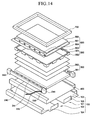
- FIG. 14 is an exploded perspective view showing a backlight assembly, according to an exemplary embodiment of the present invention.
- a board 240 including a plurality of light emitting diodes (LEDs) 241 mounted on a surface thereof is illustrated.
- the LEDs 241 face a light incident surface of a light guide plate 301 .
- First and second holder 243 , 244 are disposed in the bottom chassis 100 and fix each end portion of the board 240 .
- Wires 245 are connected to the board 240 and a driving unit providing power for driving the LEDs 241 .
- the wires 245 electrically connect the board 240 to the driving unit and deliver power to provide by a driving unit.
- the first holder 243 includes a groove for fixing one end of the board 240 .
- the second holder 244 includes a groove for fixing another end of the board 240 and a wire outlet for guiding the wires 245 .
- the wire outlet is formed on a protruding portion of the second holder 244 .
- the protruding portion is exposed outwardly from the lower surface of the bottom chassis 100 .
Landscapes
- Physics & Mathematics (AREA)
- General Physics & Mathematics (AREA)
- Optics & Photonics (AREA)
- Nonlinear Science (AREA)
- Mathematical Physics (AREA)
- Chemical & Material Sciences (AREA)
- Crystallography & Structural Chemistry (AREA)
- Planar Illumination Modules (AREA)
Abstract
Description
Claims (25)
Applications Claiming Priority (2)
| Application Number | Priority Date | Filing Date | Title |
|---|---|---|---|
| KR20080088287A KR101507737B1 (en) | 2008-09-08 | 2008-09-08 | backlight assembly and display device having the same |
| KR10-2008-0088287 | 2008-09-08 |
Publications (2)
| Publication Number | Publication Date |
|---|---|
| US20100061117A1 US20100061117A1 (en) | 2010-03-11 |
| US8206023B2 true US8206023B2 (en) | 2012-06-26 |
Family
ID=41799132
Family Applications (1)
| Application Number | Title | Priority Date | Filing Date |
|---|---|---|---|
| US12/584,520 Expired - Fee Related US8206023B2 (en) | 2008-09-08 | 2009-09-08 | Backlight assembly and display device having the same |
Country Status (2)
| Country | Link |
|---|---|
| US (1) | US8206023B2 (en) |
| KR (1) | KR101507737B1 (en) |
Cited By (4)
| Publication number | Priority date | Publication date | Assignee | Title |
|---|---|---|---|---|
| US20110222286A1 (en) * | 2010-03-12 | 2011-09-15 | Omron Corporation | Illuminating device and method for manufacturing thereof |
| US8545036B2 (en) * | 2011-11-18 | 2013-10-01 | Shenzhen China Star Optoelectronics Technology Co., Ltd. | Back frame and backlight system thereof |
| US20150131319A1 (en) * | 2013-11-11 | 2015-05-14 | Samsung Display Co., Ltd | Backlight assembly and display apparatus having the same |
| US20160120045A1 (en) * | 2014-10-23 | 2016-04-28 | Samsung Display Co., Ltd. | Display device |
Citations (8)
| Publication number | Priority date | Publication date | Assignee | Title |
|---|---|---|---|---|
| US20020034064A1 (en) * | 2000-04-07 | 2002-03-21 | Young-Su Kim | Structure for preventing wires from being damaged |
| US20030117544A1 (en) * | 2001-12-26 | 2003-06-26 | Hyo Jin Kim | Structure for assembling lamp wire for backlight assembly into liquid crystal display module |
| US20050042913A1 (en) * | 2003-08-20 | 2005-02-24 | Hong-Tien Yu | Mounting structure for lamp wires of a back light module |
| US7011443B2 (en) * | 2003-09-12 | 2006-03-14 | Quanta Display Inc. | Backlight module with side fixing frames and assembly methods thereof |
| US7048418B2 (en) * | 2001-12-26 | 2006-05-23 | Lg.Philips Lcd Co., Ltd. | Structure for holding lamp wire in liquid crystal display device |
| US7116385B2 (en) * | 2003-06-03 | 2006-10-03 | Lg.Philips Lcd Co., Ltd. | Backlight assembly with frame housing comprising a guide portion for guiding the light unit wires and liquid crystal display device having the same |
| US7190424B2 (en) * | 2003-06-10 | 2007-03-13 | Samsung Electronics Co., Ltd. | Lamp wires of a liquid crystal display secured in trenches extending at an angle to a plate sidewall |
| US7717606B2 (en) * | 2006-06-15 | 2010-05-18 | Chunghwa Picture Tubes, Ltd. | Cables fixing apparatus for backlight module |
Family Cites Families (1)
| Publication number | Priority date | Publication date | Assignee | Title |
|---|---|---|---|---|
| KR20060021074A (en) * | 2004-09-02 | 2006-03-07 | 삼성전자주식회사 | Liquid crystal display |
-
2008
- 2008-09-08 KR KR20080088287A patent/KR101507737B1/en not_active Expired - Fee Related
-
2009
- 2009-09-08 US US12/584,520 patent/US8206023B2/en not_active Expired - Fee Related
Patent Citations (9)
| Publication number | Priority date | Publication date | Assignee | Title |
|---|---|---|---|---|
| US20020034064A1 (en) * | 2000-04-07 | 2002-03-21 | Young-Su Kim | Structure for preventing wires from being damaged |
| US20030117544A1 (en) * | 2001-12-26 | 2003-06-26 | Hyo Jin Kim | Structure for assembling lamp wire for backlight assembly into liquid crystal display module |
| US7048418B2 (en) * | 2001-12-26 | 2006-05-23 | Lg.Philips Lcd Co., Ltd. | Structure for holding lamp wire in liquid crystal display device |
| US7116385B2 (en) * | 2003-06-03 | 2006-10-03 | Lg.Philips Lcd Co., Ltd. | Backlight assembly with frame housing comprising a guide portion for guiding the light unit wires and liquid crystal display device having the same |
| US7190424B2 (en) * | 2003-06-10 | 2007-03-13 | Samsung Electronics Co., Ltd. | Lamp wires of a liquid crystal display secured in trenches extending at an angle to a plate sidewall |
| US20050042913A1 (en) * | 2003-08-20 | 2005-02-24 | Hong-Tien Yu | Mounting structure for lamp wires of a back light module |
| US7011443B2 (en) * | 2003-09-12 | 2006-03-14 | Quanta Display Inc. | Backlight module with side fixing frames and assembly methods thereof |
| US7717606B2 (en) * | 2006-06-15 | 2010-05-18 | Chunghwa Picture Tubes, Ltd. | Cables fixing apparatus for backlight module |
| US7810966B2 (en) * | 2006-06-15 | 2010-10-12 | Chunghwa Picture Tubes, Ltd. | Cables fixing apparatus for backlight module |
Cited By (9)
| Publication number | Priority date | Publication date | Assignee | Title |
|---|---|---|---|---|
| US20110222286A1 (en) * | 2010-03-12 | 2011-09-15 | Omron Corporation | Illuminating device and method for manufacturing thereof |
| US8491157B2 (en) * | 2010-03-12 | 2013-07-23 | Omron Corporation | Illuminating device and method for manufacturing thereof |
| US8545036B2 (en) * | 2011-11-18 | 2013-10-01 | Shenzhen China Star Optoelectronics Technology Co., Ltd. | Back frame and backlight system thereof |
| US20150131319A1 (en) * | 2013-11-11 | 2015-05-14 | Samsung Display Co., Ltd | Backlight assembly and display apparatus having the same |
| KR20150054307A (en) * | 2013-11-11 | 2015-05-20 | 삼성디스플레이 주식회사 | Back light assembly and display apparatus having the same |
| US9354382B2 (en) * | 2013-11-11 | 2016-05-31 | Samsung Display Co., Ltd. | Backlight assembly and display apparatus having the same |
| KR102073649B1 (en) | 2013-11-11 | 2020-02-06 | 삼성디스플레이 주식회사 | Back light assembly and display apparatus having the same |
| US20160120045A1 (en) * | 2014-10-23 | 2016-04-28 | Samsung Display Co., Ltd. | Display device |
| US9746702B2 (en) * | 2014-10-23 | 2017-08-29 | Samsung Display Co., Ltd. | Display device |
Also Published As
| Publication number | Publication date |
|---|---|
| KR20100029481A (en) | 2010-03-17 |
| KR101507737B1 (en) | 2015-04-03 |
| US20100061117A1 (en) | 2010-03-11 |
Similar Documents
| Publication | Publication Date | Title |
|---|---|---|
| US8430551B2 (en) | Display apparatus and method of assembling the same | |
| US9329330B2 (en) | Backlight unit and liquid crystal display having the same | |
| US7607805B2 (en) | Backlight assembly and liquid crystal display thereof | |
| US8021034B2 (en) | Backlight assembly and display device having the same | |
| US7887210B2 (en) | Display apparatus and method of assembling the same | |
| US20090080148A1 (en) | Device and manufacturing method thereof | |
| US20080002099A1 (en) | Multilevel tool tree | |
| US9482914B2 (en) | Liquid crystal display and display apparatus set having the same | |
| US20020034064A1 (en) | Structure for preventing wires from being damaged | |
| US8734001B2 (en) | Backlight assembly including a light source cover including a sidewall cover portion which contacts with an exterior surface of a sidewall of a receiving container and a light source cover portion which covers a light source and a portion of the exiting surface of a light guide plate, display device having the same and method of assembling the display device | |
| KR20090100201A (en) | Liquid Crystal Display and Manufacturing Method Thereof | |
| KR20120030802A (en) | Liquid crystal display module and liquid crystal display device having the same | |
| US8648851B2 (en) | Liquid crystal display device | |
| US8206023B2 (en) | Backlight assembly and display device having the same | |
| US7298433B2 (en) | Liquid crystal display module having structure for preventing wires from being damaged and method of fabricating the same | |
| US7567315B2 (en) | Liquid crystal display module including hook assembly | |
| US8049857B2 (en) | Liquid crystal display device | |
| KR101245086B1 (en) | Backlight unit and liquid crystal display device having thereof | |
| KR20150130210A (en) | Display apparatus | |
| CN101114079A (en) | Backlight assembly and display device with the backlight assembly | |
| US8537306B2 (en) | Backlight assembly for liquid crystal display | |
| US20060158714A1 (en) | Wire fixing member and display device having the same | |
| KR20070115318A (en) | LCD Display | |
| KR20050040954A (en) | Liquid crystal display device module | |
| KR20070074383A (en) | LCD Display |
Legal Events
| Date | Code | Title | Description |
|---|---|---|---|
| AS | Assignment |
Owner name: SAMSUNG ELECTRONICS CO., LTD.,KOREA, REPUBLIC OF Free format text: ASSIGNMENT OF ASSIGNORS INTEREST;ASSIGNORS:KANG, SANG-MIN;SON, JUN-HEE;KIM, JYEONG-MIN;REEL/FRAME:023249/0933 Effective date: 20090904 Owner name: SAMSUNG ELECTRONICS CO., LTD., KOREA, REPUBLIC OF Free format text: ASSIGNMENT OF ASSIGNORS INTEREST;ASSIGNORS:KANG, SANG-MIN;SON, JUN-HEE;KIM, JYEONG-MIN;REEL/FRAME:023249/0933 Effective date: 20090904 |
|
| FEPP | Fee payment procedure |
Free format text: PAYOR NUMBER ASSIGNED (ORIGINAL EVENT CODE: ASPN); ENTITY STATUS OF PATENT OWNER: LARGE ENTITY |
|
| AS | Assignment |
Owner name: SAMSUNG DISPLAY CO., LTD., KOREA, REPUBLIC OF Free format text: ASSIGNMENT OF ASSIGNORS INTEREST;ASSIGNOR:SAMSUNG ELECTRONICS CO., LTD.;REEL/FRAME:029008/0876 Effective date: 20120904 |
|
| REMI | Maintenance fee reminder mailed | ||
| LAPS | Lapse for failure to pay maintenance fees | ||
| STCH | Information on status: patent discontinuation |
Free format text: PATENT EXPIRED DUE TO NONPAYMENT OF MAINTENANCE FEES UNDER 37 CFR 1.362 |
|
| STCH | Information on status: patent discontinuation |
Free format text: PATENT EXPIRED DUE TO NONPAYMENT OF MAINTENANCE FEES UNDER 37 CFR 1.362 |
|
| FP | Lapsed due to failure to pay maintenance fee |
Effective date: 20160626 |