US8102948B2 - Carrier recovery apparatus and method thereof - Google Patents
Carrier recovery apparatus and method thereof Download PDFInfo
- Publication number
- US8102948B2 US8102948B2 US12/393,023 US39302309A US8102948B2 US 8102948 B2 US8102948 B2 US 8102948B2 US 39302309 A US39302309 A US 39302309A US 8102948 B2 US8102948 B2 US 8102948B2
- Authority
- US
- United States
- Prior art keywords
- input signal
- pilot
- carrier recovery
- lock loop
- control signal
- Prior art date
- Legal status (The legal status is an assumption and is not a legal conclusion. Google has not performed a legal analysis and makes no representation as to the accuracy of the status listed.)
- Expired - Fee Related, expires
Links
- 238000011084 recovery Methods 0.000 title claims abstract description 61
- 238000000034 method Methods 0.000 title claims description 14
- 238000010586 diagram Methods 0.000 description 4
- 238000005562 fading Methods 0.000 description 4
- 230000002238 attenuated effect Effects 0.000 description 3
- 238000012986 modification Methods 0.000 description 2
- 230000004048 modification Effects 0.000 description 2
- 230000004075 alteration Effects 0.000 description 1
- 238000004891 communication Methods 0.000 description 1
Images


Classifications
-
- H—ELECTRICITY
- H04—ELECTRIC COMMUNICATION TECHNIQUE
- H04L—TRANSMISSION OF DIGITAL INFORMATION, e.g. TELEGRAPHIC COMMUNICATION
- H04L27/00—Modulated-carrier systems
- H04L27/0014—Carrier regulation
-
- H—ELECTRICITY
- H04—ELECTRIC COMMUNICATION TECHNIQUE
- H04L—TRANSMISSION OF DIGITAL INFORMATION, e.g. TELEGRAPHIC COMMUNICATION
- H04L27/00—Modulated-carrier systems
- H04L27/0014—Carrier regulation
- H04L2027/0024—Carrier regulation at the receiver end
-
- H—ELECTRICITY
- H04—ELECTRIC COMMUNICATION TECHNIQUE
- H04L—TRANSMISSION OF DIGITAL INFORMATION, e.g. TELEGRAPHIC COMMUNICATION
- H04L27/00—Modulated-carrier systems
- H04L27/0014—Carrier regulation
- H04L2027/0044—Control loops for carrier regulation
- H04L2027/0053—Closed loops
- H04L2027/0055—Closed loops single phase
-
- H—ELECTRICITY
- H04—ELECTRIC COMMUNICATION TECHNIQUE
- H04L—TRANSMISSION OF DIGITAL INFORMATION, e.g. TELEGRAPHIC COMMUNICATION
- H04L27/00—Modulated-carrier systems
- H04L27/0014—Carrier regulation
- H04L2027/0044—Control loops for carrier regulation
- H04L2027/0063—Elements of loops
- H04L2027/0067—Phase error detectors
-
- H—ELECTRICITY
- H04—ELECTRIC COMMUNICATION TECHNIQUE
- H04L—TRANSMISSION OF DIGITAL INFORMATION, e.g. TELEGRAPHIC COMMUNICATION
- H04L27/00—Modulated-carrier systems
- H04L27/0014—Carrier regulation
- H04L2027/0044—Control loops for carrier regulation
- H04L2027/0071—Control of loops
- H04L2027/0073—Detection of synchronisation state
-
- H—ELECTRICITY
- H04—ELECTRIC COMMUNICATION TECHNIQUE
- H04L—TRANSMISSION OF DIGITAL INFORMATION, e.g. TELEGRAPHIC COMMUNICATION
- H04L27/00—Modulated-carrier systems
- H04L27/0014—Carrier regulation
- H04L2027/0044—Control loops for carrier regulation
- H04L2027/0071—Control of loops
- H04L2027/0079—Switching between loops
-
- H—ELECTRICITY
- H04—ELECTRIC COMMUNICATION TECHNIQUE
- H04L—TRANSMISSION OF DIGITAL INFORMATION, e.g. TELEGRAPHIC COMMUNICATION
- H04L27/00—Modulated-carrier systems
- H04L27/0014—Carrier regulation
- H04L2027/0083—Signalling arrangements
- H04L2027/0085—Signalling arrangements with no special signals for synchronisation
-
- H—ELECTRICITY
- H04—ELECTRIC COMMUNICATION TECHNIQUE
- H04L—TRANSMISSION OF DIGITAL INFORMATION, e.g. TELEGRAPHIC COMMUNICATION
- H04L27/00—Modulated-carrier systems
- H04L27/0014—Carrier regulation
- H04L2027/0083—Signalling arrangements
- H04L2027/0087—Out-of-band signals, (e.g. pilots)
Definitions
- the present invention relates to a carrier recovery apparatus and a related method, and more particularly, to a carrier recovery apparatus and a related method selectively allowing a pilot-based FPLL or a pilot-less PLL to perform the carrier recovery on an input signal according to a pilot strength of the input signal.
- a pilot is purposely added to facilitate carrier recovery at the receiver side.
- a conventional pilot-based frequency and phase lock loop is typically used to achieve both wide acquisition range and fast acquisition speed.
- FPLL frequency and phase lock loop
- a carrier recovery apparatus includes a pilot strength detector, a first lock loop, a second lock loop, and a controller.
- the pilot strength detector determines whether a pilot strength of an input signal is greater than a threshold value to generate a control signal.
- the first lock loop performs a first carrier recovery on the input signal.
- the second lock loop performs a second carrier recovery on the input signal.
- the controller selectively allows the first lock loop to perform the first carrier recovery on the input signal or the second lock loop to perform the second carrier recovery on the input signal according to the control signal.
- the first lock loop is a pilot-based FPLL and the second locked loop is a pilot-less PLL.
- a method for carrier recovery includes the step of determining whether a pilot strength of an input signal is greater than a threshold value to generate a control signal; and selectively allowing a pilot-based FPLL to perform a first carrier recovery on the input signal or a pilot-less PLL to perform a second carrier recovery on the input signal according to the control signal.
- the control signal indicates that the pilot strength of the input signal is greater than the threshold value
- the pilot-less PLL when the control signal indicates that the pilot strength of the input signal is not greater than the threshold value, allow the pilot-less PLL to perform the second carrier recovery on the input signal.
- FIG. 1 is a diagram of a carrier recovery apparatus according to a first embodiment of the present invention.
- FIG. 2 is a diagram of a carrier recovery apparatus according to a second embodiment of the present invention.
- FIG. 3 is a flowchart illustrating a method for carrier recovery according to an embodiment of the present invention.
- FIG. 1 is a diagram of a carrier recovery apparatus 100 according to a first embodiment of the present invention.
- the carrier recovery apparatus 100 includes, but is not limited to, a pilot strength detector 110 , a pilot-based frequency and phase lock loop (FPLL) 130 , a pilot-less phase lock loop (PLL) 140 , and a controller 120 .
- the pilot strength detector 110 determines whether a pilot strength of an input signal SIN is greater than a threshold value TH 1 to generate a control signal SC.
- the pilot-based FPLL 130 performs a first carrier recovery on the input signal SIN.
- the pilot-less PLL 140 performs a second carrier recovery on the input signal SIN.
- the controller 120 is coupled to the pilot strength detector 110 , the pilot-based FPLL 130 , and the pilot-less PLL 140 for selectively allowing the pilot-based FPLL 130 to perform the first carrier recovery on the input signal SIN or the pilot-less PLL 140 to perform the second carrier recovery on the input signal SIN according to the control signal SC.
- the controller 120 allows the pilot-based FPLL 130 to perform the first carrier recovery on the input signal SIN.
- the controller 120 allows the pilot-less PLL 140 to perform the second carrier recovery on the input signal SIN.
- the controller 140 can determine to allow the pilot-based FPLL 130 or the pilot-less PLL 140 to perform the carrier recovery on the input signal SIN according to the pilot strength of the input signal SIN.
- the pilot-less PLL 140 will replace the pilot-based FPLL 130 to perform the carrier recovery on the input signal, which can avoid the problem of losing lock and causing disruption in reception to improve the whole system stability.
- the pilot-less PLL is more implementation-friendly than the conventional pilot-less FPLL, which lowers the complexity and saves the cost.
- pilot-based FPLL 130 and the pilot-less PLL 140 can be digitally implemented, but is not limited to this and can be analogically implemented.
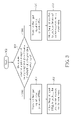
- FIG. 2 is a diagram of a carrier recovery apparatus 200 according to a second embodiment of the present invention.
- the architecture of the carrier recovery apparatus 200 is similar to that in FIG. 1 , the difference being that the controller of the carrier recovery apparatus 200 is a selector 220 .
- the selector 220 is implemented by a switch SW 1 , but this should not be considered as a limitation of the present invention.
- the selector 220 has an input end 221 for receiving the input signal SIN, a control end 222 coupled to the pilot strength detector 110 for receiving the control signal SC, a first output end 223 coupled to the pilot-based FPLL 130 , and a second output end 224 coupled to the pilot-less PLL 140 .
- the selector 220 transmits the input signal SIN to the pilot-based FPLL 130 when the control signal SC indicates that the pilot strength of the input signal SIN is greater than the threshold value TH 1 ; otherwise, the selector 220 transmits the input signal SIN to the pilot-less PLL 140 .
- the threshold value TH 1 is not a fixed value, and can be adjusted depending on practical demands, such as the channel status or the standard of the received input signal SIN.
- FIG. 3 is a flowchart illustrating a method for carrier recovery according to an embodiment of the present invention. Please note that the following steps are not limited to be performed according to the exact sequence shown in FIG. 3 if a roughly identical result can be obtained.
- the method includes, but is not limited to, the following steps:
- Step 302 Start.
- Step 304 Determine whether a pilot strength of an input signal is greater than a threshold value to generate a control signal.
- Step 310 Transmit the input signal to the pilot-based FPLL.
- Step 312 Allow the pilot-based FPLL to perform the first carrier recovery on the input signal.
- Step 320 Transmit the input signal to the pilot-less PLL.
- Step 322 Allow the pilot-less PLL to perform the second carrier recovery on the input signal.
- Step 304 the pilot strength detector 110 determines whether the pilot strength of the input signal SIN is greater than the threshold value TH 1 to generate the control signal SC. If the pilot strength of the input signal SIN is greater than the threshold value TH 1 , execute the steps 310 and 312 ; otherwise, go to the steps 320 and 322 .
- the controller 120 or the selector 220 transmits the input signal SIN to the pilot-based FPLL 130 and allows it to perform the first carrier recovery on the input signal SIN (the steps 310 and 312 ).
- the controller 120 or the selector 220 transmits the input signal SIN to the pilot-less PLL 140 and allows it to perform the second carrier recovery on the input signal SIN (the steps 320 and 322 ).
- steps of the method shown in FIG. 3 need not be in the exact order shown and need not be contiguous: other steps can be intermediate.
- the present invention provides a carrier recovery apparatus and a related method.
- the carrier recovery apparatus disclosed in the present invention combines a pilot-based FPLL or a pilot-less PLL, and determines when to allow the pilot-based FPLL or the pilot-less PLL to perform the carrier recovery on the input signal SIN according to the pilot strength of the input signal SIN. Therefore, the problem of losing lock and causing disruption in reception can be avoided to improve the whole system stability even if the pilot is severely attenuated or even notched due to fading.
- the pilot-less PLL disclosed in the present invention is more implementation-friendly than the conventional pilot-less FPLL, which lowers the complexity and saves the cost.
- the threshold value TH 1 of the pilot strength detector can be adjusted depending on practical channel status or the standard of the received input signal SIN, so as to be applied to various situations.
Landscapes
- Engineering & Computer Science (AREA)
- Computer Networks & Wireless Communication (AREA)
- Signal Processing (AREA)
- Stabilization Of Oscillater, Synchronisation, Frequency Synthesizers (AREA)
Abstract
Description
Claims (6)
Priority Applications (1)
| Application Number | Priority Date | Filing Date | Title |
|---|---|---|---|
| US12/393,023 US8102948B2 (en) | 2009-02-25 | 2009-02-25 | Carrier recovery apparatus and method thereof |
Applications Claiming Priority (1)
| Application Number | Priority Date | Filing Date | Title |
|---|---|---|---|
| US12/393,023 US8102948B2 (en) | 2009-02-25 | 2009-02-25 | Carrier recovery apparatus and method thereof |
Publications (2)
| Publication Number | Publication Date |
|---|---|
| US20100215126A1 US20100215126A1 (en) | 2010-08-26 |
| US8102948B2 true US8102948B2 (en) | 2012-01-24 |
Family
ID=42630950
Family Applications (1)
| Application Number | Title | Priority Date | Filing Date |
|---|---|---|---|
| US12/393,023 Expired - Fee Related US8102948B2 (en) | 2009-02-25 | 2009-02-25 | Carrier recovery apparatus and method thereof |
Country Status (1)
| Country | Link |
|---|---|
| US (1) | US8102948B2 (en) |
Cited By (1)
| Publication number | Priority date | Publication date | Assignee | Title |
|---|---|---|---|---|
| US20130321049A1 (en) * | 2012-06-01 | 2013-12-05 | Samsung Electronics Co., Ltd. | Smart card clock generator circuits wth autonomous operation capability and method of operating the same |
Families Citing this family (2)
| Publication number | Priority date | Publication date | Assignee | Title |
|---|---|---|---|---|
| US8792590B2 (en) * | 2009-02-25 | 2014-07-29 | Harris Corporation | Communications device with in-phase/quadrature (I/Q) DC offset, gain and phase imbalance compensation and related method |
| JP2015220613A (en) * | 2014-05-16 | 2015-12-07 | 株式会社東芝 | Wireless receiver |
Citations (1)
| Publication number | Priority date | Publication date | Assignee | Title |
|---|---|---|---|---|
| US7558340B2 (en) * | 2003-12-01 | 2009-07-07 | Lg Electronics Inc. | VSB receiver and carrier recovery apparatus thereof |
-
2009
- 2009-02-25 US US12/393,023 patent/US8102948B2/en not_active Expired - Fee Related
Patent Citations (1)
| Publication number | Priority date | Publication date | Assignee | Title |
|---|---|---|---|---|
| US7558340B2 (en) * | 2003-12-01 | 2009-07-07 | Lg Electronics Inc. | VSB receiver and carrier recovery apparatus thereof |
Cited By (2)
| Publication number | Priority date | Publication date | Assignee | Title |
|---|---|---|---|---|
| US20130321049A1 (en) * | 2012-06-01 | 2013-12-05 | Samsung Electronics Co., Ltd. | Smart card clock generator circuits wth autonomous operation capability and method of operating the same |
| US8836388B2 (en) * | 2012-06-01 | 2014-09-16 | Samsung Electronics Co., Ltd. | Smart card clock generator circuits wth autonomous operation capability and method of operating the same |
Also Published As
| Publication number | Publication date |
|---|---|
| US20100215126A1 (en) | 2010-08-26 |
Similar Documents
| Publication | Publication Date | Title |
|---|---|---|
| US6763229B2 (en) | Timing recovery switching for an adaptive digital broadband beamforming (antenna diversity) for ATSC terrestrial DTV based on segment sync detection | |
| US8422983B2 (en) | Method of controlling power consumption for a radio receiver | |
| US8284853B2 (en) | Apparatus and method for spatial multiplexing with backward compatibility in a multiple input multiple output wireless communication system | |
| US8768285B2 (en) | Synchronization of front-end and baseband units in wireless communications device by wirelessly transmitting clock signal therebetween | |
| US20080123724A1 (en) | Signal processing circuit | |
| US8311155B2 (en) | Electronic tuner and high frequency receiving device using the same | |
| US8102948B2 (en) | Carrier recovery apparatus and method thereof | |
| US8493907B2 (en) | Frequency offset estimation scheme in scheduled based wireless system | |
| US8045649B2 (en) | Carrier recovery system and carrier recovery method | |
| JP4133190B2 (en) | Gain control method for receiving signals transmitted in bursts and receiver using the same | |
| US20120099683A1 (en) | Demodulation device | |
| US9148855B2 (en) | Receiver and communication apparatus | |
| US20110117859A1 (en) | Wireless communication device, wireless communication method, program, and integrated circuit | |
| KR102000439B1 (en) | Antenna swtiching apparatus of spatial modulation | |
| JP4329793B2 (en) | Radio receiving apparatus and radio communication system | |
| US6745017B2 (en) | Timing recovery switching for an adaptive digital broadband beamforming (antenna diversity) for ATSC terrestrial DTV based on a differentiator | |
| KR101577183B1 (en) | Diversity receiving device and diversity receiving method thereof | |
| CN105553534B (en) | Signal processing method, device and baseband processing chip | |
| JP5691186B2 (en) | Automatic frequency control device and radio communication device | |
| CN101478329B (en) | Method, apparatus and system for selecting path | |
| JP2006135724A (en) | Receiver | |
| US8929837B2 (en) | Signal processing system and method thereof | |
| JP3059995U (en) | Tuner device | |
| CN101841502A (en) | Carrier recovery device and related method | |
| JP3334667B2 (en) | Space diversity receiver circuit |
Legal Events
| Date | Code | Title | Description |
|---|---|---|---|
| AS | Assignment |
Owner name: HIMAX MEDIA SOLUTIONS, INC., TAIWAN Free format text: ASSIGNMENT OF ASSIGNORS INTEREST;ASSIGNORS:GAU, GUO-HAU;SHIH, PEI-JUN;CHENG, SHIN-SHIUAN;REEL/FRAME:022313/0390 Effective date: 20090216 |
|
| ZAAA | Notice of allowance and fees due |
Free format text: ORIGINAL CODE: NOA |
|
| ZAAB | Notice of allowance mailed |
Free format text: ORIGINAL CODE: MN/=. |
|
| STCF | Information on status: patent grant |
Free format text: PATENTED CASE |
|
| FPAY | Fee payment |
Year of fee payment: 4 |
|
| MAFP | Maintenance fee payment |
Free format text: PAYMENT OF MAINTENANCE FEE, 8TH YEAR, LARGE ENTITY (ORIGINAL EVENT CODE: M1552); ENTITY STATUS OF PATENT OWNER: LARGE ENTITY Year of fee payment: 8 |
|
| AS | Assignment |
Owner name: HIMAX TECHNOLOGIES LIMITED, TAIWAN Free format text: MERGER;ASSIGNOR:HIMAX MEDIA SOLUTIONS, INC.;REEL/FRAME:060501/0001 Effective date: 20220503 |
|
| FEPP | Fee payment procedure |
Free format text: MAINTENANCE FEE REMINDER MAILED (ORIGINAL EVENT CODE: REM.); ENTITY STATUS OF PATENT OWNER: LARGE ENTITY |
|
| LAPS | Lapse for failure to pay maintenance fees |
Free format text: PATENT EXPIRED FOR FAILURE TO PAY MAINTENANCE FEES (ORIGINAL EVENT CODE: EXP.); ENTITY STATUS OF PATENT OWNER: LARGE ENTITY |
|
| STCH | Information on status: patent discontinuation |
Free format text: PATENT EXPIRED DUE TO NONPAYMENT OF MAINTENANCE FEES UNDER 37 CFR 1.362 |
|
| FP | Lapsed due to failure to pay maintenance fee |
Effective date: 20240124 |