US8101970B2 - Semiconductor device - Google Patents
Semiconductor device Download PDFInfo
- Publication number
- US8101970B2 US8101970B2 US12/539,617 US53961709A US8101970B2 US 8101970 B2 US8101970 B2 US 8101970B2 US 53961709 A US53961709 A US 53961709A US 8101970 B2 US8101970 B2 US 8101970B2
- Authority
- US
- United States
- Prior art keywords
- diffusion region
- parasitic bjt
- well
- bjt
- semiconductor device
- Prior art date
- Legal status (The legal status is an assumption and is not a legal conclusion. Google has not performed a legal analysis and makes no representation as to the accuracy of the status listed.)
- Active, expires
Links
Images


Classifications
-
- H—ELECTRICITY
- H10—SEMICONDUCTOR DEVICES; ELECTRIC SOLID-STATE DEVICES NOT OTHERWISE PROVIDED FOR
- H10D—INORGANIC ELECTRIC SEMICONDUCTOR DEVICES
- H10D84/00—Integrated devices formed in or on semiconductor substrates that comprise only semiconducting layers, e.g. on Si wafers or on GaAs-on-Si wafers
- H10D84/80—Integrated devices formed in or on semiconductor substrates that comprise only semiconducting layers, e.g. on Si wafers or on GaAs-on-Si wafers characterised by the integration of at least one component covered by groups H10D12/00 or H10D30/00, e.g. integration of IGFETs
- H10D84/82—Integrated devices formed in or on semiconductor substrates that comprise only semiconducting layers, e.g. on Si wafers or on GaAs-on-Si wafers characterised by the integration of at least one component covered by groups H10D12/00 or H10D30/00, e.g. integration of IGFETs of only field-effect components
- H10D84/83—Integrated devices formed in or on semiconductor substrates that comprise only semiconducting layers, e.g. on Si wafers or on GaAs-on-Si wafers characterised by the integration of at least one component covered by groups H10D12/00 or H10D30/00, e.g. integration of IGFETs of only field-effect components of only insulated-gate FETs [IGFET]
- H10D84/85—Complementary IGFETs, e.g. CMOS
- H10D84/854—Complementary IGFETs, e.g. CMOS comprising arrangements for preventing bipolar actions between the different IGFET regions, e.g. arrangements for latchup prevention
-
- H—ELECTRICITY
- H10—SEMICONDUCTOR DEVICES; ELECTRIC SOLID-STATE DEVICES NOT OTHERWISE PROVIDED FOR
- H10D—INORGANIC ELECTRIC SEMICONDUCTOR DEVICES
- H10D84/00—Integrated devices formed in or on semiconductor substrates that comprise only semiconducting layers, e.g. on Si wafers or on GaAs-on-Si wafers
- H10D84/80—Integrated devices formed in or on semiconductor substrates that comprise only semiconducting layers, e.g. on Si wafers or on GaAs-on-Si wafers characterised by the integration of at least one component covered by groups H10D12/00 or H10D30/00, e.g. integration of IGFETs
- H10D84/811—Combinations of field-effect devices and one or more diodes, capacitors or resistors
Definitions
- the present invention relates to a semiconductor device, and more particularly, to a semiconductor device that can prevent the latch-up phenomenon from happening.
- FIG. 1 shows a simplified diagram of a conventional semiconductor device 100 .
- the semiconductor device 100 comprises: a P type semiconductor substrate 102 , an N-well 104 , a first P+ diffusion region 106 , a first N+ diffusion region 108 , a second N+ diffusion region 110 , a second P+ diffusion region 112 , a third P+ diffusion region 114 , a first insulation layer 116 , a second insulation layer 118 , a first parasitic bipolar junction transistor (BJT) 120 , and a second parasitic BJT 122 .
- the N-well 104 is positioned in the P type semiconductor substrate 102 .
- the first P+ diffusion region 106 is positioned in the N-well 104 .
- the first P+ diffusion region 106 is coupled to an input signal VDD 1 .
- the first N+ diffusion region 108 and the second N+ diffusion region 110 are positioned in the N-well 104 , and utilized for coupled to a voltage source VDD 2 , respectively.
- the second P+ diffusion region 112 and the third P+ diffusion region 114 are positioned in the P type semiconductor substrate 102 , and utilized for coupled to a voltage level VSS 1 , respectively.
- the first insulation layer 116 is positioned between the first N+ diffusion region 108 and the second P+ diffusion region 112 .
- the second insulation layer 118 is positioned between the second N+ diffusion region 110 and the third P+ diffusion region 114 .
- the first parasitic BJT 120 has an emitter, a base, and a collector, wherein the emitter of the first parasitic BJT 120 is formed by the first P+ diffusion region 106 , the base of the first parasitic BJT 120 is formed by the N-well 104 connected to the first N+ diffusion region 108 , and the collector of the first parasitic BJT 120 is formed by the P type semiconductor substrate 102 connected to the second P+ diffusion region 112 .
- the second parasitic BJT 122 has an emitter, a base, and a collector, wherein the emitter of the second parasitic BJT 122 is formed by the first P+ diffusion region 106 , the base of the second parasitic BJT 122 is formed by the N-well 104 connected to the second N+ diffusion region 110 , and the collector of the second parasitic BJT 122 is formed by the P type semiconductor substrate 102 connected to the third P+ diffusion region 114 .
- FIG. 2 shows a timing diagram of the voltage level VSS 1 , the input signal VDD 1 , and the voltage source VDD 2 in FIG. 1 .
- the voltage level lifting speed of the input signal VDD 1 is faster than the voltage level lifting speed of the voltage source VDD 2 , and thus when the voltage level of the input signal VDD 1 is higher than the voltage level of the voltage source VDD 2 , the first parasitic BJT 120 and the second parasitic BJT 122 will be conducted, and a latch-up phenomenon will appear. In this way, a large current will be generated to damage the semiconductor device 100 easily.
- a semiconductor device comprises: a P type semiconductor substrate, an N-well, a first P+ diffusion region, a second P+ diffusion region, a Schottky diode, a first N+ diffusion region, a second N+ diffusion region, a third P+ diffusion region, a fourth P+ diffusion region, a first insulation layer, a second insulation layer, a first parasitic bipolar junction transistor (BJT), and a second parasitic BJT.
- the N-well is positioned in the P type semiconductor substrate.
- the first P+ diffusion region and the second P+ diffusion region are positioned in the N-well.
- the Schottky diode is positioned in the N-well, and utilized for coupled to an input signal.
- the first N+ diffusion region and the second N+ diffusion region are positioned in the N-well, and utilized for coupled to a voltage source, respectively.
- the third P+ diffusion region and the fourth P+ diffusion region are positioned in the P type semiconductor substrate.
- the first insulation layer is positioned between the first N+ diffusion region and the third P+ diffusion region.
- the second insulation layer is positioned between the second N+ diffusion region and the fourth P+ diffusion region.
- the first parasitic BJT has an emitter, a base, and a collector, wherein the emitter of the first parasitic BJT is formed by the first P+ diffusion region, the base of the first parasitic BJT is formed by the N-well connected to the first N+ diffusion region, and the collector of the first parasitic BJT is formed by the P type semiconductor substrate connected to the third P+ diffusion region.
- the second parasitic BJT has an emitter, a base, and a collector, wherein the emitter of the second parasitic BJT is formed by the second P+ diffusion region, the base of the second parasitic BJT is formed by the N-well connected to the second N+ diffusion region, and the collector of the second parasitic BJT is formed by the P type semiconductor substrate connected to the fourth P+ diffusion region.
- the Schottky diode conducts charges to make the first parasitic BJT and the second parasitic BJT not conducted.
- a semiconductor device comprises: a N type semiconductor substrate, an P-well, a first N+ diffusion region, a second N+ diffusion region, a Schottky diode, a first P+ diffusion region, a second P+ diffusion region, a third N+ diffusion region, a fourth N+ diffusion region, a first insulation layer, a second insulation layer, a first parasitic bipolar junction transistor (BJT), and a second parasitic BJT.
- the P-well is positioned in the N type semiconductor substrate.
- the first N+ diffusion region and the second N+ diffusion region are positioned in the P-well.
- the Schottky diode is positioned in the P-well, and utilized for coupled to an input signal.
- the first P+ diffusion region and the second P+ diffusion region are positioned in the P-well, and utilized for coupled to a voltage source, respectively.
- the third N+ diffusion region and the fourth N+ diffusion region are positioned in the N type semiconductor substrate.
- the first insulation layer is positioned between the first P+ diffusion region and the third N+ diffusion region.
- the second insulation layer is positioned between the second P+ diffusion region and the fourth N+ diffusion region.
- the first parasitic BJT has an emitter, a base, and a collector, wherein the emitter of the first parasitic BJT is formed by the first N+ diffusion region, the base of the first parasitic BJT is formed by the P-well connected to the first P+ diffusion region, and the collector of the first parasitic BJT is formed by the N type semiconductor substrate connected to the third N+ diffusion region.
- the second parasitic BJT has an emitter, a base, and a collector, wherein the emitter of the second parasitic BJT is formed by the second N+ diffusion region, the base of the second parasitic BJT is formed by the P-well connected to the second P+ diffusion region, and the collector of the second parasitic BJT is formed by the N type semiconductor substrate connected to the fourth N+ diffusion region.
- the Schottky diode conducts charges to make the first parasitic BJT and the second parasitic BJT not conducted.
- the semiconductor device disclosed by the present invention can prevent the latch-up phenomenon from happening, and thus it is not easy for the semiconductor device of the present invention to be damaged, and the semiconductor device of the present invention has a longer lifetime.
- FIG. 1 shows a simplified diagram of a conventional semiconductor device.
- FIG. 2 shows a timing diagram of the voltage level VSS 1 , the input signal VDD 1 , and the voltage source VDD 2 in FIG. 1 .
- FIG. 3 shows a simplified diagram of a semiconductor device in accordance with a first embodiment of the present invention.
- FIG. 4 shows a timing diagram of the voltage level VSS 1 , the input signal VDD 1 , and the voltage source VDD 2 in the first embodiment of the present invention.
- FIG. 5 shows a simplified diagram of a semiconductor device in accordance with a second embodiment of the present invention.
- FIG. 6 shows a timing diagram of the voltage level VSS 1 , the input signal VDD 1 , and the voltage source VDD 2 in the second embodiment of the present invention.
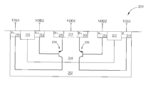
- FIG. 3 shows a simplified diagram of a semiconductor device 200 in accordance with a first embodiment of the present invention, wherein the semiconductor device 200 is fabricated by a logic process.
- the semiconductor device 200 comprises: a P type semiconductor substrate 202 , an N-well 204 , a first P+ diffusion region 206 , a second P+ diffusion region 208 , a Schottky diode 210 , a first N+ diffusion region 212 , a second N+ diffusion region 214 , a third P+ diffusion region 216 , a fourth P+ diffusion region 218 , a first insulation layer 220 , a second insulation layer 222 , a first parasitic bipolar junction transistor (BJT) 224 , and a second parasitic BJT 226 .
- BJT bipolar junction transistor
- the N-well 204 is positioned in the P type semiconductor substrate 202 .
- the first P+ diffusion region 206 and the second P+ diffusion region 208 are positioned in the N-well 204 .
- the Schottky diode 210 is positioned between the first P+ diffusion region 206 and the second P+ diffusion region 208 , and utilized for coupled to an input signal VDD 1 .
- the first N+ diffusion region 212 and the second N+ diffusion region 214 are positioned in the N-well 204 , and utilized for coupled to a voltage source VDD 2 , respectively.
- the third P+ diffusion region 216 and the fourth P+ diffusion region 218 are positioned in the P type semiconductor substrate 202 , and utilized for coupled to a voltage level VSS 1 , respectively.
- the first insulation layer 220 is positioned between the first N+ diffusion region 212 and the third P+ diffusion region 216 .
- the second insulation layer 222 is positioned between the second N+ diffusion region 214 and the fourth P+ diffusion region 218 .
- the first parasitic BJT 224 has an emitter, a base, and a collector, wherein the emitter of the first parasitic BJT 224 is formed by the first P+ diffusion region 206 , the base of the first parasitic BJT 224 is formed by the N-well 204 connected to the first N+ diffusion region 212 , and the collector of the first parasitic BJT 224 is formed by the P type semiconductor substrate 202 connected to the third P+ diffusion region 216 .
- the second parasitic BJT 226 has an emitter, a base, and a collector, wherein the emitter of the second parasitic BJT 226 is formed by the second P+ diffusion region 208 , the base of the second parasitic BJT 226 is formed by the N-well 204 connected to the second N+ diffusion region 214 , and the collector of the second parasitic BJT 226 is formed by the P type semiconductor substrate 202 connected to the fourth P+ diffusion region 218 .
- the above embodiment is only for an illustrative purpose and is not meant to be a limitation of the present invention.
- the Schottky diode 210 is not limited to be positioned between the first P+ diffusion region 206 and the second P+ diffusion region 208 , and the Schottky diode 210 also can be positioned in other positions of the N-well 204 .
- FIG. 4 shows a timing diagram of the voltage level VSS 1 , the input signal VDD 1 , and the voltage source VDD 2 in the first embodiment of the present invention. As shown in FIG. 4 , the voltage level lifting speed of the input signal VDD 1 is faster than the voltage level lifting speed of the voltage source VDD 2 .
- the forward bias threshold voltage of the Schottky diode 210 in the semiconductor device 200 of the present invention (such as 0.4V) is lower than the forward bias threshold voltages of the first parasitic BJT 224 and the second parasitic BJT 226 (such as 0.7V), and thus when the voltage level of the input signal VDD 1 is higher than the voltage level of the voltage source VDD 2 , the present invention can utilize the Schottky diode 210 to conduct charges so as to make the first parasitic BJT 224 and the second parasitic BJT 226 not conducted.
- the semiconductor device 200 of the present invention can prevent the latch-up phenomenon from happening, and thus it is not easy for the semiconductor device 200 of the present invention to be damaged, and the semiconductor device 200 of the present invention has a longer lifetime.
- the above embodiment is only for an illustrative purpose and is not meant to be a limitation of the present invention.
- the concept of the present invention also can be utilized in the semiconductor devices fabricated by other semiconductor processes (such as a high voltage process).
- FIG. 5 shows a simplified diagram of a semiconductor device 300 in accordance with a second embodiment of the present invention, wherein the semiconductor device 300 is fabricated by a logic process.
- the semiconductor device 300 comprises: a N type semiconductor substrate 302 , an P-well 304 , a first N+ diffusion region 306 , a second N+ diffusion region 308 , a Schottky diode 310 , a first P+ diffusion region 312 , a second P+ diffusion region 314 , a third N+ diffusion region 316 , a fourth N+ diffusion region 318 , a first insulation layer 320 , a second insulation layer 322 , a first parasitic BJT 324 , and a second parasitic BJT 326 .
- the P-well 304 is positioned in the N type semiconductor substrate 302 .
- the first N+ diffusion region 306 and the second N+ diffusion region 308 are positioned in the P-well 304 .
- the Schottky diode 310 is positioned in the P-well 304 , and utilized for coupled to an input signal VDD 1 .
- the first P+ diffusion region 312 and the second P+ diffusion region 314 are positioned in the P-well 304 , and utilized for coupled to a voltage source VDD 2 , respectively.
- the third N+ diffusion region 316 and the fourth N+ diffusion region 318 are positioned in the N type semiconductor substrate 302 , and utilized for coupled to a voltage level VSS 1 , respectively.
- the first insulation layer 320 is positioned between the first P+ diffusion region 312 and the third N+ diffusion region 316 .
- the second insulation layer 322 is positioned between the second P+ diffusion region 314 and the fourth N+ diffusion region 318 .
- the first parasitic BJT 324 has an emitter, a base, and a collector, wherein the emitter of the first parasitic BJT 324 is formed by the first N+ diffusion region 306 , the base of the first parasitic BJT 324 is formed by the P-well 304 connected to the first P+ diffusion region 312 , and the collector of the first parasitic BJT 324 is formed by the N type semiconductor substrate 302 connected to the third N+ diffusion region 316 .
- the second parasitic BJT 326 has an emitter, a base, and a collector, wherein the emitter of the second parasitic BJT 326 is formed by the second N+ diffusion region 308 , the base of the second parasitic BJT 326 is formed by the P-well 304 connected to the second P+ diffusion region 314 , and the collector of the second parasitic BJT 326 is formed by the N type semiconductor substrate 302 connected to the fourth N+ diffusion region 318 .
- the Schottky diode 310 conducts charges to make the first parasitic BJT 324 and the second parasitic BJT 326 not conducted.
- the Schottky diode 310 is not limited to be positioned between the first P+ diffusion region 306 and the second P+ diffusion region 308 , and the Schottky diode 310 also can be positioned in other positions of the N-well 304 .
- FIG. 6 shows a timing diagram of the voltage level VSS 1 , the input signal VDD 1 , and the voltage source VDD 2 in the second embodiment of the present invention. As shown in FIG. 6 , the voltage level descending speed of the input signal VDD 1 is faster than the voltage level descending speed of the voltage source VDD 2 .
- the forward bias threshold voltage of the Schottky diode 310 in the semiconductor device 300 of the present invention is higher than the forward bias threshold voltages of the first parasitic BJT 324 and the second parasitic BJT 326 , and thus when the voltage level of the input signal VDD 1 is lower than the voltage level of the voltage source VDD 2 , the present invention can utilize the Schottky diode 310 to conduct charges so as to make the first parasitic BJT 324 and the second parasitic BJT 326 not conducted. In this way, the semiconductor device 300 of the present invention can prevent the latch-up phenomenon from happening, and thus it is not easy for the semiconductor device 300 of the present invention to be damaged, and the semiconductor device 300 of the present invention has a longer lifetime.
- the semiconductor device disclosed by the present invention can prevent the latch-up phenomenon from happening, and thus it is not easy for the semiconductor device of the present invention to be damaged, and the semiconductor device of the present invention has a longer lifetime.
Landscapes
- Metal-Oxide And Bipolar Metal-Oxide Semiconductor Integrated Circuits (AREA)
- Semiconductor Integrated Circuits (AREA)
- Electrodes Of Semiconductors (AREA)
Abstract
Description
Claims (8)
Applications Claiming Priority (3)
| Application Number | Priority Date | Filing Date | Title |
|---|---|---|---|
| TW098123217 | 2009-07-09 | ||
| TW98123217A | 2009-07-09 | ||
| TW098123217A TWI482264B (en) | 2009-07-09 | 2009-07-09 | Semiconductor device |
Publications (2)
| Publication Number | Publication Date |
|---|---|
| US20110006396A1 US20110006396A1 (en) | 2011-01-13 |
| US8101970B2 true US8101970B2 (en) | 2012-01-24 |
Family
ID=43426839
Family Applications (1)
| Application Number | Title | Priority Date | Filing Date |
|---|---|---|---|
| US12/539,617 Active 2030-10-14 US8101970B2 (en) | 2009-07-09 | 2009-08-12 | Semiconductor device |
Country Status (3)
| Country | Link |
|---|---|
| US (1) | US8101970B2 (en) |
| JP (1) | JP5219972B2 (en) |
| TW (1) | TWI482264B (en) |
Citations (2)
| Publication number | Priority date | Publication date | Assignee | Title |
|---|---|---|---|---|
| US6784489B1 (en) * | 1997-03-28 | 2004-08-31 | Stmicroelectronics, Inc. | Method of operating a vertical DMOS transistor with schottky diode body structure |
| US20100208399A1 (en) * | 2009-02-17 | 2010-08-19 | Jing-Chi Yu | Electrostatic discharge protection circuit |
Family Cites Families (3)
| Publication number | Priority date | Publication date | Assignee | Title |
|---|---|---|---|---|
| JP2954242B2 (en) * | 1989-09-20 | 1999-09-27 | 株式会社日立製作所 | Integrated circuit device |
| JP2843393B2 (en) * | 1989-12-29 | 1999-01-06 | 沖電気工業株式会社 | Multi-level output circuit |
| KR100504204B1 (en) * | 2003-04-01 | 2005-07-27 | 매그나칩 반도체 유한회사 | Method for manufacturing bipolar transistor by using cmos process |
-
2009
- 2009-07-09 TW TW098123217A patent/TWI482264B/en active
- 2009-08-12 US US12/539,617 patent/US8101970B2/en active Active
- 2009-09-11 JP JP2009210089A patent/JP5219972B2/en active Active
Patent Citations (2)
| Publication number | Priority date | Publication date | Assignee | Title |
|---|---|---|---|---|
| US6784489B1 (en) * | 1997-03-28 | 2004-08-31 | Stmicroelectronics, Inc. | Method of operating a vertical DMOS transistor with schottky diode body structure |
| US20100208399A1 (en) * | 2009-02-17 | 2010-08-19 | Jing-Chi Yu | Electrostatic discharge protection circuit |
Also Published As
| Publication number | Publication date |
|---|---|
| JP2011155025A (en) | 2011-08-11 |
| JP5219972B2 (en) | 2013-06-26 |
| TW201103122A (en) | 2011-01-16 |
| TWI482264B (en) | 2015-04-21 |
| US20110006396A1 (en) | 2011-01-13 |
Similar Documents
| Publication | Publication Date | Title |
|---|---|---|
| US10134723B2 (en) | Electrostatic discharge protection device and electronic device having the same | |
| US8405943B2 (en) | Circuit and method for power clamp triggered dual SCR ESD protection | |
| US7554839B2 (en) | Symmetric blocking transient voltage suppressor (TVS) using bipolar transistor base snatch | |
| US7880223B2 (en) | Latch-up free vertical TVS diode array structure using trench isolation | |
| US7034363B2 (en) | Bi-directional EOS/ESD protection device | |
| US7755143B2 (en) | Semiconductor device | |
| US10930641B2 (en) | Series connected ESD protection circuit | |
| US20190363076A1 (en) | Electrostatic discharge protection semiconductor device | |
| US12136621B2 (en) | Bidirectional electrostatic discharge (ESD) protection device | |
| US20160285262A1 (en) | Electrostatic discharge protection circuit | |
| KR100243496B1 (en) | Semiconductor device | |
| JP2015103605A (en) | ESD protection circuit | |
| CN102208412B (en) | SCR structure used for ESD protection of integrated circuit output stage | |
| US11652097B2 (en) | Transient voltage suppression device | |
| US6940104B2 (en) | Cascaded diode structure with deep N-well and method for making the same | |
| US11742657B2 (en) | Electrostatic discharge protection circuit | |
| US11222886B2 (en) | ESD protection device with low trigger voltage | |
| US8101970B2 (en) | Semiconductor device | |
| US20100208399A1 (en) | Electrostatic discharge protection circuit | |
| US20120313095A1 (en) | Electrostatic discharge protection circuit employing polysilicon diode | |
| US7960785B2 (en) | Semiconductor integrated circuit devices | |
| US20140002934A1 (en) | Latch-up immune esd protection | |
| US20080121925A1 (en) | Low voltage triggered silicon controlled rectifier | |
| CN101958320B (en) | Semiconductor device | |
| US20110156211A1 (en) | Semiconductor structure for realizing esd protection circuit |
Legal Events
| Date | Code | Title | Description |
|---|---|---|---|
| AS | Assignment |
Owner name: ILI TECHNOLOGY CORP., TAIWAN Free format text: ASSIGNMENT OF ASSIGNORS INTEREST;ASSIGNORS:YU, JING-CHI;LU, YU-LUN;REEL/FRAME:023088/0108 Effective date: 20090803 |
|
| STCF | Information on status: patent grant |
Free format text: PATENTED CASE |
|
| FEPP | Fee payment procedure |
Free format text: PAT HOLDER NO LONGER CLAIMS SMALL ENTITY STATUS, ENTITY STATUS SET TO UNDISCOUNTED (ORIGINAL EVENT CODE: STOL); ENTITY STATUS OF PATENT OWNER: LARGE ENTITY |
|
| FPAY | Fee payment |
Year of fee payment: 4 |
|
| AS | Assignment |
Owner name: MRISE TECHNOLOGY INC., TAIWAN Free format text: MERGER;ASSIGNOR:ILI TECHNOLOGY CORP.;REEL/FRAME:040688/0263 Effective date: 20150826 |
|
| AS | Assignment |
Owner name: ILI TECHNOLOGY CORP., TAIWAN Free format text: CHANGE OF NAME;ASSIGNOR:MRISE TECHNOLOGY INC.;REEL/FRAME:040676/0700 Effective date: 20161220 |
|
| MAFP | Maintenance fee payment |
Free format text: PAYMENT OF MAINTENANCE FEE, 8TH YEAR, LARGE ENTITY (ORIGINAL EVENT CODE: M1552); ENTITY STATUS OF PATENT OWNER: LARGE ENTITY Year of fee payment: 8 |
|
| AS | Assignment |
Owner name: ILI TECHNOLOGY HOLDING CORPORATION, CAYMAN ISLANDS Free format text: ASSIGNMENT OF ASSIGNORS INTEREST;ASSIGNOR:ILI TECHNOLOGY CORP.;REEL/FRAME:055257/0614 Effective date: 20201210 |
|
| AS | Assignment |
Owner name: ILI TECHNOLOGY CORP., TAIWAN Free format text: ASSIGNMENT OF ASSIGNORS INTEREST;ASSIGNOR:ILI TECHNOLOGY HOLDING CORPORATION;REEL/FRAME:060262/0911 Effective date: 20220322 |
|
| MAFP | Maintenance fee payment |
Free format text: PAYMENT OF MAINTENANCE FEE, 12TH YEAR, LARGE ENTITY (ORIGINAL EVENT CODE: M1553); ENTITY STATUS OF PATENT OWNER: LARGE ENTITY Year of fee payment: 12 |