US8099792B1 - Methods and apparatus for spatially resolved photocurrent mapping of operating photovoltaic devices using atomic force photovoltaic microscopy - Google Patents
Methods and apparatus for spatially resolved photocurrent mapping of operating photovoltaic devices using atomic force photovoltaic microscopy Download PDFInfo
- Publication number
- US8099792B1 US8099792B1 US12/319,454 US31945409A US8099792B1 US 8099792 B1 US8099792 B1 US 8099792B1 US 31945409 A US31945409 A US 31945409A US 8099792 B1 US8099792 B1 US 8099792B1
- Authority
- US
- United States
- Prior art keywords
- component
- photovoltaic
- photocurrent
- tip
- conductive
- Prior art date
- Legal status (The legal status is an assumption and is not a legal conclusion. Google has not performed a legal analysis and makes no representation as to the accuracy of the status listed.)
- Expired - Fee Related, expires
Links
Images


Classifications
-
- G—PHYSICS
- G01—MEASURING; TESTING
- G01Q—SCANNING-PROBE TECHNIQUES OR APPARATUS; APPLICATIONS OF SCANNING-PROBE TECHNIQUES, e.g. SCANNING PROBE MICROSCOPY [SPM]
- G01Q60/00—Particular types of SPM [Scanning Probe Microscopy] or microscopes; Essential components thereof
- G01Q60/24—AFM [Atomic Force Microscopy] or apparatus therefor, e.g. AFM probes
- G01Q60/30—Scanning potential microscopy
-
- B—PERFORMING OPERATIONS; TRANSPORTING
- B82—NANOTECHNOLOGY
- B82Y—SPECIFIC USES OR APPLICATIONS OF NANOSTRUCTURES; MEASUREMENT OR ANALYSIS OF NANOSTRUCTURES; MANUFACTURE OR TREATMENT OF NANOSTRUCTURES
- B82Y10/00—Nanotechnology for information processing, storage or transmission, e.g. quantum computing or single electron logic
-
- B—PERFORMING OPERATIONS; TRANSPORTING
- B82—NANOTECHNOLOGY
- B82Y—SPECIFIC USES OR APPLICATIONS OF NANOSTRUCTURES; MEASUREMENT OR ANALYSIS OF NANOSTRUCTURES; MANUFACTURE OR TREATMENT OF NANOSTRUCTURES
- B82Y35/00—Methods or apparatus for measurement or analysis of nanostructures
-
- H—ELECTRICITY
- H10—SEMICONDUCTOR DEVICES; ELECTRIC SOLID-STATE DEVICES NOT OTHERWISE PROVIDED FOR
- H10K—ORGANIC ELECTRIC SOLID-STATE DEVICES
- H10K71/00—Manufacture or treatment specially adapted for the organic devices covered by this subclass
- H10K71/70—Testing, e.g. accelerated lifetime tests
-
- H—ELECTRICITY
- H10—SEMICONDUCTOR DEVICES; ELECTRIC SOLID-STATE DEVICES NOT OTHERWISE PROVIDED FOR
- H10K—ORGANIC ELECTRIC SOLID-STATE DEVICES
- H10K30/00—Organic devices sensitive to infrared radiation, light, electromagnetic radiation of shorter wavelength or corpuscular radiation
- H10K30/30—Organic devices sensitive to infrared radiation, light, electromagnetic radiation of shorter wavelength or corpuscular radiation comprising bulk heterojunctions, e.g. interpenetrating networks of donor and acceptor material domains
-
- H—ELECTRICITY
- H10—SEMICONDUCTOR DEVICES; ELECTRIC SOLID-STATE DEVICES NOT OTHERWISE PROVIDED FOR
- H10K—ORGANIC ELECTRIC SOLID-STATE DEVICES
- H10K39/00—Integrated devices, or assemblies of multiple devices, comprising at least one organic radiation-sensitive element covered by group H10K30/00
-
- H—ELECTRICITY
- H10—SEMICONDUCTOR DEVICES; ELECTRIC SOLID-STATE DEVICES NOT OTHERWISE PROVIDED FOR
- H10K—ORGANIC ELECTRIC SOLID-STATE DEVICES
- H10K85/00—Organic materials used in the body or electrodes of devices covered by this subclass
- H10K85/10—Organic polymers or oligomers
- H10K85/111—Organic polymers or oligomers comprising aromatic, heteroaromatic, or aryl chains, e.g. polyaniline, polyphenylene or polyphenylene vinylene
- H10K85/113—Heteroaromatic compounds comprising sulfur or selene, e.g. polythiophene
-
- H—ELECTRICITY
- H10—SEMICONDUCTOR DEVICES; ELECTRIC SOLID-STATE DEVICES NOT OTHERWISE PROVIDED FOR
- H10K—ORGANIC ELECTRIC SOLID-STATE DEVICES
- H10K85/00—Organic materials used in the body or electrodes of devices covered by this subclass
- H10K85/20—Carbon compounds, e.g. carbon nanotubes or fullerenes
- H10K85/211—Fullerenes, e.g. C60
- H10K85/215—Fullerenes, e.g. C60 comprising substituents, e.g. PCBM
-
- Y—GENERAL TAGGING OF NEW TECHNOLOGICAL DEVELOPMENTS; GENERAL TAGGING OF CROSS-SECTIONAL TECHNOLOGIES SPANNING OVER SEVERAL SECTIONS OF THE IPC; TECHNICAL SUBJECTS COVERED BY FORMER USPC CROSS-REFERENCE ART COLLECTIONS [XRACs] AND DIGESTS
- Y02—TECHNOLOGIES OR APPLICATIONS FOR MITIGATION OR ADAPTATION AGAINST CLIMATE CHANGE
- Y02E—REDUCTION OF GREENHOUSE GAS [GHG] EMISSIONS, RELATED TO ENERGY GENERATION, TRANSMISSION OR DISTRIBUTION
- Y02E10/00—Energy generation through renewable energy sources
- Y02E10/50—Photovoltaic [PV] energy
- Y02E10/549—Organic PV cells
Definitions
- ⁇ p The performance of organic photovoltaic (OPV) devices is most frequently characterized by the power conversion efficiency, ⁇ p , which indicates the percentage of the radiant energy incident on the solar cell that is converted to electrical energy, and is determined by measuring the open-circuit voltage (V oc ), short-circuit current (I sc ), and fill factor from current-voltage plots.
- V oc open-circuit voltage
- I sc short-circuit current
- ⁇ p serves as a convenient benchmark for comparing photovoltaic devices, it does not reveal information about local photocurrent spatial variations within these devices.
- BHJ bulk-heterojunction
- Atomic force microscopy is described generally in U.S. Pat. No. 6,642,517, the entirety of which—and, in particular, FIGS. 1-2, 4 and 6-7 and corresponding descriptions thereof and the references cited therein—is incorporated herein by reference. More specifically, conductive atomic force microscopy (cAFM) has recently proven to be an effective method for probing current flow and resistivity variations with nanometer scale spatial resolution in gold nanowires, silicon field effect transistors, individual organic molecules, conducting polymer blends, and emissive polymers. See, respectively: M. C. Hersam, A. C. F. Hoole, S. J. O'Shea, and M. E. Welland, Appl. Phys. Lett. 72, 915 (1998); P.
- cAFM conductive atomic force microscopy
- cAFM can directly correlate optoelectronic stimulation with nanometer scale spatial resolution. With appropriate collection optics and photon detectors, the resulting photocurrent can be spatially correlated with the cAFM tip position, thus enabling nanometer scale photocurrent mapping.
- cAFM is described generally in U.S. Pat. No. 5,874,734, the entirety of which is incorporated hereby by reference.
- cAFM and analogous scanning tunneling microscopy measurements have been used to spatially map current in a variety of organic materials.
- the conductive tip was brought directly into contact with the organic material. Again, while such direct electrical contact with the materials is sufficient to induce current, a point contact of this type is inevitably different from the evaporated electrical contacts fabricated in actual photovoltaic devices.
- this invention can be directed to a method of using conductive atomic force microscopy for photocurrent characterization of a photovoltaic device.
- a method can comprise providing an operative photovoltaic device comprising an anode, a cathode and at least one optoelectric component therebetween; illuminating such a device; contacting the device and/or an electrode thereof with a conductive atomic force microscope comprising a biased current conductive cantilever tip; and correlating photocurrent and/or various aspects thereof (e.g., without limitation, power conversion efficiency) with position of the conductive tip on the illuminated device. Illumination can be at least partially sufficient to generate and/or induce photocurrent.
- the conductive tip can be at a constant bias and/or at a fixed position on an electrode for photocurrent characterization, in particular to detect and/or measure current-voltage characteristics.
- current generation and light conversion can be detected as a function of illumination.
- a bias can be applied over and/or along a surface of such a device. Accordingly, such a device can be topographically mapped. In certain such embodiments, current generation and/or light conversion can be mapped simultaneously with device topography.
- bias and/or application such a device can comprise a solar cell. With bias applied over and/or along such a cell, current generation and/or light conversion can be detected as a function of distance. Regardless of device composition, function or utility, bias can be applied over and/or along a device surface. In certain such embodiments, spatial variations of power conversion efficiency can be correlated with illumination.
- this invention can also be directed to a conductive atomic microscope apparatus for spatial resolution of a photocurrent characteristic of a photovoltaic device.
- a conductive atomic microscope apparatus for spatial resolution of a photocurrent characteristic of a photovoltaic device.
- Such an apparatus can comprise a probe comprising a current conductive cantilever tip; an optics component opposite such a cantilever tip and comprising a solar light simulator and a lens arranged and configured to direct light to a photovoltaic device; and a photodetection component aligned with the cantilever tip and such an optics component for photocurrent detection and analysis.
- such an apparatus can comprise a scanner component.
- such a scanner component can be vertically-aligned with a photodetection component.
- such an apparatus can comprise an operative or operating photovoltaic device positioned between an optics component and the cantilever tip.
- such a device can comprise a solar cell. Demonstrating a length-scale which can be associated with this invention, resolution can be realized with a solar cell comprising a surface area less than about 5 ⁇ m 2 . Regardless of surface area or dimension, such a solar cell can comprise an optoelectric component selected from an organic material, an inorganic material, an organic-inorganic hybrid material, and combinations thereof.
- this invention can also be directed to a method for spatial-resolution of a photocurrent characteristic of a photovoltaic device.
- a method can comprise providing an operative photovoltaic device comprising an array of solar cells, each such cell comprising an anode, a cathode and at least one optoelectric component therebetween; contacting such a device with a conductive atomic force microscope apparatus, such an apparatus comprising a biased current conductive cantilever tip, an optics component and a scanner, such a device positioned between the cantilever tip and an optics component, with such a bias applied over and/or along a surface of such a device; illuminating such a device with an optics component; and correlating photocurrent of the illuminated device with cantilever tip position thereon.
- current generation and/or light conversion can be mapped simultaneously with device topography.
- spatial variations of power conversion efficiency can be correlated with illumination.
- FIG. 1 A non-limiting schematic diagram of an atomic force photovoltaic microscope (AFPM) apparatus, in accordance with certain embodiments of this invention.
- AFPM atomic force photovoltaic microscope
- FIGS. 2A-C (A) AFPM topographic map of a 7.5 ⁇ m ⁇ 7.5 ⁇ m OPV array. (B) AFPM current map at 0.0 V applied bias and (C) AFPM current map at ⁇ 0.50 V applied bias. In the AFPM current maps, the absolute value of the photocurrent is depicted.
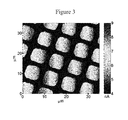
- FIG. 3 Short-circuit transient response of OPV devices in air. Devices are illuminated at 6.7 suns and are first contacted at the left edge. Note that the absolute value of the photocurrent is depicted and that the current scale bar is truncated compared to FIG. 2 .
- FIGS. 4A and 4B Photocurrent maps of 60 ⁇ m 2 electrodes (A) and 3 ⁇ m 2 electrodes (B).
- Various embodiments of this invention provide an alternative cAFM technique, atomic force photovoltaic microscopy (AFPM), which can quantitatively characterize variations in fully operational photovoltaic devices; e.g., without limitation, by scanning one or an array of solar cells. Analyzing devices more closely reproduces real-world operating conditions, enables standard photovoltaic figures of merit to be extracted, minimizes substrate-cAFM tip contact effects and—more generally—provides nanoscale characterization of a wide range of optoelectronically-active materials and devices.
- FAM atomic force photovoltaic microscopy
- FIG. 1 A schematic illustration of an apparatus 10 , in accordance with this invention, is provided in FIG. 1 .
- Scanning can be accomplished under ambient conditions, using a commercially-available cAFM, modified as described herein. More specifically, a conventional cantilever beam deflection component 12 detects deflection of probe assembly 14 as conducting tip 16 interacts with a surface of a photovoltaic device.
- Sample/device 1 e.g., without limitation, an OPV device
- Apparatus 10 includes a laser 18 for directing a beam of light toward cantilever 12 which, during operation, interacts with and reflects the laser toward photodetector 20 .
- apparatus 10 measures the position of the deflected light beam which is indicative of the deflection of cantilever component 12 which, in turn, is a measure of the reaction force between tip 14 and the device surface. More specifically to the apparatus of FIG. 1 , a positive bias can be applied while tip 16 is connected to current preamplifier 22 acting as a virtual ground.
- optics stage 24 is designed to support optics component 26 .
- Light from solar simulator 28 is focused by convex lens 30 and mirror 32 toward the device of sample/device 1 .
- implementation of the methodologies and techniques of this invention is not restricted to the specific components recited herein.
- various other apparatus configurations can be used, as would be understood by those skilled in the art made aware of this invention. Nonetheless, an apparatus of this invention can be assembled and configured with components commercially available and used in conjunction with various other cAFM applications. See, e.g., the apparatus/component configurations described in the references incorporated herein.
- the glass substrate with the photovoltaic devices is attached to a lightweight ( ⁇ 5 g) optics stage.
- AFEM atomic force electroluminescence
- the stage is fabricated from plastic fasteners, and its small mass minimizes interference with the piezoelectric scanner on which it rests. All experiments were performed in contact-mode and ambient conditions on a ThermoMicroscopes CP Research AFM with Nanosensors boron-doped, diamond-coated silicon AFM probes (model DT-NCHR). Electrical connection is made to the indium-tin-oxide (ITO) anode by affixing a copper wire, and a DL Instruments current preamplifier measures the current through the cAFM probe, which scans across the array of cathodes at an applied force of 20-50 nN. Although the short-circuit current is typically on the order of 10 nA for these devices, currents ⁇ 1 pA can be measured.
- ITO indium-tin-oxide
- a DL Instruments current preamplifier measures the current through the cAFM probe, which scans across the array of cathodes at an applied force of 20-50 nN
- ITO-coated glass sheet resistance ⁇ 10 ⁇ /sq, RMS roughness ⁇ 2.5 nm
- Delta Technologies served as the substrate for all devices characterized.
- the substrates are cleaned with a standard detergent/deionized water/solvent sonication process and then treated with UV-ozone or an O 2 -plasma.
- P3HT was purchased from Rieke Metals and the PCBM from American Dye Source; both were purified by standard techniques.
- AFPM was used to characterize spatially localized inhomogeneities in OPV devices.
- a biased cAFM probe can be raster-scanned over an array of illuminated solar cells, simultaneously generating topographic and photocurrent maps.
- AFPM was used to characterize 7.5 ⁇ m ⁇ 7.5 ⁇ m poly(3-hexylthiophene):[6,6]-phenyl-C 61 -butyric acid methyl ester (P3HT:PCBM) OPVs, revealing substantial device-to-device and temporal variations in the short-circuit current.
- the ITO substrates are treated with O 2 -plasma and then spin-coated with PEDOT:PSS for 30 s at 2800 rpm to deposit a 41-45 nm film.
- the substrates are transferred to a glove box ( ⁇ 1 ppm O 2 ) and then spin-coated with a 1:1 solution of P3HT:PCBM dissolved in purified 1,2-dichlorobenze.
- the P3HT:PCBM solution is spin-coated onto the PEDOT:PSS layer for 60 s at 550 rpm, allowed to dry in the glove box, and then annealed at ⁇ 110° C. Although such devices are often dried slowly in covered Petri dishes, the shorter drying times used here ( ⁇ 5 min) reduce film roughness and significantly improve the probe-sample contact.
- the BHJ film was deposited under the same conditions, but the ITO was UV-ozone cleaned.
- 7.5 ⁇ m ⁇ 7.5 ⁇ m gold cathodes were then thermally evaporated through a copper mesh TEM grid (Ted Pella, Inc) at 0.2-0.3 ⁇ /s to a thickness of ⁇ 50 nm on the P3HT:PCBM film.
- Gold was initially used as the cathode material because of its resistance to oxidation under the ambient test conditions.
- FIG. 2 shows simultaneous AFPM topography-current maps from P3HT:PCBM OPVs fabricated without a PEDOT:PSS layer.
- the current maps in FIGS. 2( b ) and 2 ( c ) were collected sequentially from the same set scan area, with the sample bias changed from 0.0 V (I sc ) in the former to ⁇ 0.50 V in the latter.
- Devices were illuminated at ⁇ 6.7 suns in both scans. The scans show similar device-to-device variations, including a difference in I sc up to ⁇ 25% between OPVs separated by ⁇ 10 ⁇ m.
- solar cells can also be individually addressed by the cAFM probe to measure current-voltage characteristics.
- These devices exhibit S-shaped I-V plots and low fill factors ( ⁇ 18.5%), characteristic of marginal active layer/cathode interfaces. (This behavior may be attributable to LiF not applied prior to gold deposition and because the deposition conditions are significantly harsher for gold than for aluminum.)
- the devices exhibit a short-circuit current density of ⁇ 18 mA/cm 2 (under 6.7 suns illumination), an open-circuit voltage of ⁇ 225 mV, and a power conversion efficiency of ⁇ 0.11%.
- AFPM probes the performance of functioning devices instead of the film itself, a notable point because the probe-sample interaction impacts the current signal in cAFM.
- the conductive probe scans a rough surface (such as a phase-separated photovoltaic film), and the contact area between the probe and sample are likely continuously changing.
- the resulting current map can be a convolution of the true electrical properties of the sample and the variable sample-probe contact.
- FIG. 4 compares a current map with the aforementioned 7.5 ⁇ m ⁇ 7.5 ⁇ m devices (A) with smaller ⁇ 2 ⁇ m diameter devices (B) fabricated using a holey carbon film.
- the improved resolution provides additional information about spatially localized photocurrent variations within a sample, with the image in FIG. 4B exhibiting a much broader range of current variation than the image in FIG. 4A .
- Resolution can be improved even further with devices smaller than 1 ⁇ m 2 , as can be fabricated from commercially available holey carbon films.
- AFPM AFPM methods, apparatus and related techniques of this invention can be used to quantitatively measure spatial performance variations in operative, functioning photovoltaic devices. For instance, microscopic solar cells can be individually addressed, enabling quantification of local ⁇ p and other benchmarks. Furthermore, temporal variations in photovoltaic response can be directly visualized.
- the flexibility of AFPM permits use over a range of applications. For instance, a photovoltaic device can be characterized by evaluating defect density and ⁇ p as a function of device area. These and various other characterizations can be made in conjunction with increasing spatial resolution through the use of smaller electrodes.
- Other applications include evaluating devices fabricated with alternative (e.g., transparent) electrodes and/or different photoactive (e.g., organic, inorganic and/or organic-inorganic hybrid) layers to elucidate performance-spatial relationships in photovoltaic cells and/or to assure quality control during fabrication.
- alternative e.g., transparent
- photoactive e.g., organic, inorganic and/or organic-inorganic hybrid
Landscapes
- Engineering & Computer Science (AREA)
- Chemical & Material Sciences (AREA)
- Nanotechnology (AREA)
- Physics & Mathematics (AREA)
- Health & Medical Sciences (AREA)
- Crystallography & Structural Chemistry (AREA)
- Manufacturing & Machinery (AREA)
- General Health & Medical Sciences (AREA)
- General Physics & Mathematics (AREA)
- Nuclear Medicine, Radiotherapy & Molecular Imaging (AREA)
- Radiology & Medical Imaging (AREA)
- Analytical Chemistry (AREA)
- Mathematical Physics (AREA)
- Theoretical Computer Science (AREA)
- Photovoltaic Devices (AREA)
Abstract
Description
Claims (19)
Priority Applications (1)
| Application Number | Priority Date | Filing Date | Title |
|---|---|---|---|
| US12/319,454 US8099792B1 (en) | 2008-01-07 | 2009-01-07 | Methods and apparatus for spatially resolved photocurrent mapping of operating photovoltaic devices using atomic force photovoltaic microscopy |
Applications Claiming Priority (2)
| Application Number | Priority Date | Filing Date | Title |
|---|---|---|---|
| US1029308P | 2008-01-07 | 2008-01-07 | |
| US12/319,454 US8099792B1 (en) | 2008-01-07 | 2009-01-07 | Methods and apparatus for spatially resolved photocurrent mapping of operating photovoltaic devices using atomic force photovoltaic microscopy |
Publications (1)
| Publication Number | Publication Date |
|---|---|
| US8099792B1 true US8099792B1 (en) | 2012-01-17 |
Family
ID=45445204
Family Applications (1)
| Application Number | Title | Priority Date | Filing Date |
|---|---|---|---|
| US12/319,454 Expired - Fee Related US8099792B1 (en) | 2008-01-07 | 2009-01-07 | Methods and apparatus for spatially resolved photocurrent mapping of operating photovoltaic devices using atomic force photovoltaic microscopy |
Country Status (1)
| Country | Link |
|---|---|
| US (1) | US8099792B1 (en) |
Cited By (4)
| Publication number | Priority date | Publication date | Assignee | Title |
|---|---|---|---|---|
| US8884247B2 (en) * | 2012-09-25 | 2014-11-11 | Fei Company | System and method for ex situ analysis of a substrate |
| US9139908B2 (en) | 2013-12-12 | 2015-09-22 | The Boeing Company | Gradient thin films |
| US9508944B2 (en) | 2012-04-11 | 2016-11-29 | The Boeing Company | Composite organic-inorganic energy harvesting devices and methods |
| WO2019104254A1 (en) * | 2017-11-22 | 2019-05-31 | South Dakota State University (Sdsu) | Atomic force microscope based instrumentation for probing nanoscale charge carrier dynamics with improved temporal and spatial resolution |
Citations (11)
| Publication number | Priority date | Publication date | Assignee | Title |
|---|---|---|---|---|
| US5196701A (en) * | 1991-07-31 | 1993-03-23 | International Business Machines Corporation | High-resolution detection of material property variations |
| US5874734A (en) | 1996-12-31 | 1999-02-23 | Elings; Virgil B. | Atomic force microscope for measuring properties of dielectric and insulating layers |
| US6198097B1 (en) * | 1998-04-15 | 2001-03-06 | The United States Of America As Represented By The Secretary Of The Army | Photocharge microscope |
| US6690008B2 (en) * | 2000-09-15 | 2004-02-10 | Interuniversitair Microelektronica Centrum (Imec) | Probe and method of manufacturing mounted AFM probes |
| US6787768B1 (en) * | 2001-03-08 | 2004-09-07 | General Nanotechnology Llc | Method and apparatus for tool and tip design for nanomachining and measurement |
| US20050030054A1 (en) * | 2003-06-17 | 2005-02-10 | Mao-Nan Chang | Electrical scanning probe microscope apparatus |
| US6861648B2 (en) * | 1994-07-28 | 2005-03-01 | General Nanotechnology Llc | Scanning probe microscopy inspection and modification system |
| US7093509B2 (en) * | 2004-03-18 | 2006-08-22 | The Trustees Of The University Of Pennsylvania | Scanning probe microscopy apparatus and techniques |
| US7358490B1 (en) | 2004-05-28 | 2008-04-15 | Northwestern University | Methods and apparatus of spatially resolved electroluminescence of operating organic light-emitting diodes using conductive atomic force microscopy |
| US20100017922A1 (en) * | 2006-05-31 | 2010-01-21 | Heungjoo Shin | Integrated sensing probes, methods of fabrication thereof, and methods of use thereof |
| US20100180354A1 (en) * | 2005-10-25 | 2010-07-15 | Georgia Tech Research Corporation | Three-Dimensional Nanoscale Metrology using FIRAT Probe |
-
2009
- 2009-01-07 US US12/319,454 patent/US8099792B1/en not_active Expired - Fee Related
Patent Citations (12)
| Publication number | Priority date | Publication date | Assignee | Title |
|---|---|---|---|---|
| US5196701A (en) * | 1991-07-31 | 1993-03-23 | International Business Machines Corporation | High-resolution detection of material property variations |
| US6861648B2 (en) * | 1994-07-28 | 2005-03-01 | General Nanotechnology Llc | Scanning probe microscopy inspection and modification system |
| US5874734A (en) | 1996-12-31 | 1999-02-23 | Elings; Virgil B. | Atomic force microscope for measuring properties of dielectric and insulating layers |
| US6198097B1 (en) * | 1998-04-15 | 2001-03-06 | The United States Of America As Represented By The Secretary Of The Army | Photocharge microscope |
| US6690008B2 (en) * | 2000-09-15 | 2004-02-10 | Interuniversitair Microelektronica Centrum (Imec) | Probe and method of manufacturing mounted AFM probes |
| US6787768B1 (en) * | 2001-03-08 | 2004-09-07 | General Nanotechnology Llc | Method and apparatus for tool and tip design for nanomachining and measurement |
| US20050030054A1 (en) * | 2003-06-17 | 2005-02-10 | Mao-Nan Chang | Electrical scanning probe microscope apparatus |
| US6975129B2 (en) * | 2003-06-17 | 2005-12-13 | National Applied Research Labratories | Electrical scanning probe microscope apparatus |
| US7093509B2 (en) * | 2004-03-18 | 2006-08-22 | The Trustees Of The University Of Pennsylvania | Scanning probe microscopy apparatus and techniques |
| US7358490B1 (en) | 2004-05-28 | 2008-04-15 | Northwestern University | Methods and apparatus of spatially resolved electroluminescence of operating organic light-emitting diodes using conductive atomic force microscopy |
| US20100180354A1 (en) * | 2005-10-25 | 2010-07-15 | Georgia Tech Research Corporation | Three-Dimensional Nanoscale Metrology using FIRAT Probe |
| US20100017922A1 (en) * | 2006-05-31 | 2010-01-21 | Heungjoo Shin | Integrated sensing probes, methods of fabrication thereof, and methods of use thereof |
Non-Patent Citations (26)
| Title |
|---|
| Alexeev, A; Loos, J; Koetse, MM. Nanoscale electrical characterization of semiconducting polymer blends by conductive atomic force microscopy (C-AFM). Ultramicroscopy 106 (2006) 191-199. |
| Coffey, DC; Ginger, DS. Time-resolved electrostatic force microscopy of polymer solar cells. Nature Materials, vol. 5, Sep. 2006, pp. 735-740. |
| Coffey, DC; Reid, OG; Radovsky, DB; Bartholomew, GP; Ginger, DS. Mapping Local Photocurrents in Polymer/Fullerene Solar Cells with Photoconductive Atomic Force Microscopy. Nano Letters, 2007, Vol. 7, No. 3, pp. 738-744. |
| De Wolf, P; Vandervorst, W; Smith, H; Khalil, N. Comparison of two-dimensional carrier profiles in metal-oxide-semiconductor field-effect transistor structures obtained with scanning spreading resistance microscopy in inverse modeling. J. Vac. Sci. Technol. B 18(1), Jan./Feb. 2000. pp. 540-544. |
| Douhérat, O; Lutsen, L; Swinnen, A; Breselge, M; Vandewal, K; Goris, L; Manca, J. Nanoscale electrical characterization of organic photovoltaic blends by conductive atomic force microscopy. Applied Physics Letters, 89, 032107 (2006). |
| Gatzel, T; Hoppe, H; Sariciftci, NS; Lux-Steiner, MC; Komiyama, M. Kelvin Probe force Microscopy Study of Conjugated Polymer/Fullerene Organic Solar Cells. Japanese Journal of Applied Physics. vol. 44, No. 7B, 2005, pp. 5370-5373. |
| Glatthaar, M; Riede, M; Keegan, N; Sylvester-Hvid, K; Zimmermann, B; Niggemann, M; Hinsch, A; Gombert, A. Efficiency limited factors of organic bulk heterojunction solar cells identified by electrical impedance spectroscopy. Solar Energy Materials & Solar Cells 91 (2007) 390-393. |
| Günes, S; Neugebauer, H; Sariciftci, NS. Conjugated Polymer-Based Organic Solar Cells. Chem. Rev. 2007, 107, 1324-1338. |
| Hersam, MC; Hoole, ACF; O'Shea, SJ; Welland, ME. Potentiometry and repair of electrically stressed nanowires using atomic force microscopy. Applied Physics Letters, vol. 72, No. 8, Feb. 23, 1998. pp. 915-917. |
| Hoppe, H; Niggemann, MP; Winder, C; Kraut, J; Hiesgen, R; Hinsch, A; Meissner, D; Sariciftci, S. Nanoscale Morphology of Conjugated Polymer/Fullerene-Based Bulk-Heterojunction Solar Cells. Adv. Funct. Mater. 2004, 14, No. 10, October, pp. 1005-1011. |
| Kawano, K; Pacios, R; Poplavskyy, D; Nelson, J; Bradley, DDC; Durrant, JR. Degradation of organic solar cells due to air exposure. Solar Energy Materials & Solar Cells 90 (2006) 3520-3530. |
| Lin, H-N; Lin, H-L; Wang, SS; Yu, L-S; Perng, G-Y; Chen, S-A; Chen, S-H. Nanoscale charge transport in an electroluminescent polymer investigated by conducting atomic force microscopy. Applied Physics Letters, vol. 81, No. 14, Sep. 30, 2002, pp. 2572-2574. |
| Ma, W; Yang, C; Gong, X; Lee, K; Heeger, AJ. Thermally Stable, Efficient Polymer Solar Cells with Nanoscale Control of the Interpenetrating Network Morphology. Adv. Funct. Mater. 2005, 15, 1617-1622. |
| McNeill, CR; Dastoor, PC. Photocurrent pattern formation in polymer/methanofullerene blends imaged by near-field scanning photocurrent microscopy. Journal of Applied Physics 99, 033502 (2006). |
| McNeill, CR; Watts, B; Thomsen, L; Belcher, WJ; Greenham, NC Dastoor, PC. Nanoscale Quantitative Chemical Mapping of Conjugated Polymer Blends. Nano Letters, 2006, vol. 6, No. 6, pp. 1202-1206. |
| Mihailetchi, VD; Xie, H; De Boer, B; Popescu, LM; Hummelen, JC; Blom, PWM. Origin of the enhanced performance in poly(3-hexylthiophene): [6,6]-phenyl C61-butyric acid methyl ester solar cells upon slow drying of the active layer. Applied Physics Letters 89, 012107 (2006). |
| Moutinho, HR; Dhere, RG; Jiang, C-S; Al-Jassim, MM; Kazmerski, LL. Electrical properties of CdTe/CdS solar cells investigated with conductive atomic force microscopy. Thin Solid Films 514 (2006) 150-155. |
| Peumans, P; Yakimov, A; Forrest, SR. Small molecular weight organic thin-film photodetectors and solar cells. Journal of Applied Physics, vol. 93, No. 7, Apr. 1, 2003, pp. 3693-3723. |
| Pingree, LSC; Hersam, MC; Kern, MM; Scott, BJ; Marks, TJ. Spatially-resolved electroluminescence of operating organic light-emitting diodes using conductive atomic force microscopy. Applied Physics Letters, vol. 85, No. 2, Jul. 12, 2004, pp. 344-346. |
| Pingree, LSC; Russell, MT; Scott, BJ; Marks, TJ; Hersam, MC. Probing individual nanoscale organic light-emitting diodes with atomic force electroluminescence microscopy and bridge-enhanced nanoscale impedance microscopy. Organic Electronics 8 (2007) 465-479. |
| Planès, J; Houzé, F; Chrétien, P; Schneegans, O. Conducting probe atomic force microscopy applied to organic conducting blends. Applied Physics Letters. vol. 79, No. 18, Oct. 29, 2001. pp. 2993-2995. |
| Rashmi, AKK; Kumar, U; Balakrishnan, VR; Basu, PK. Degradation of process in organic thin film devices fabricated using P3HT. Pramana- J. Phys., vol. 68, No. 3, Mar. 2007, pp. 489-498. |
| Rawlett, AM; Hopson, TJ; Nagahara, LA; Tsui, RK; Ramachandran, GK; Lindsay, SM. Electrical measurements of a dithiolated molecule via conducting atomic force microscopy. Applied Physics Letter, vol. 81, No. 16, Oct. 14, 2002, pp. 3043-3045. |
| Smith, AP; Smith RR; Taylor, BE; Durstock, MF. An Investigation of Poly(thienylene vinylene) in Organic Photovoltaic Devices. Chem. Mater. 2004, 16, 4687-4692. |
| Snaith, HJ; Arias, AC; Morteani, AC; Silva, C; Friend, RH. Charge Generation Kinetics and Transport Mechanisms in Blended Polufluorene Photovoltaic Devices. Nano Letters, 2002, vol. 2, No. 12, pp. 1353-1357. |
| Yang, X; Loos, J; Veenstra, SC; Verhees, WJH; Wienk, MM; Kroon, JM; Michels, MAJ; Janssen, RAJ. Nanoscale Morphology of High-Performance Polymer Solar Cells. Nano Letters, 2005, vol. 5, No. 4, pp. 579-583. |
Cited By (6)
| Publication number | Priority date | Publication date | Assignee | Title |
|---|---|---|---|---|
| US9508944B2 (en) | 2012-04-11 | 2016-11-29 | The Boeing Company | Composite organic-inorganic energy harvesting devices and methods |
| US10347857B2 (en) | 2012-04-11 | 2019-07-09 | The Boeing Company | Composite organic-inorganic energy harvesting devices and methods |
| US8884247B2 (en) * | 2012-09-25 | 2014-11-11 | Fei Company | System and method for ex situ analysis of a substrate |
| US9139908B2 (en) | 2013-12-12 | 2015-09-22 | The Boeing Company | Gradient thin films |
| WO2019104254A1 (en) * | 2017-11-22 | 2019-05-31 | South Dakota State University (Sdsu) | Atomic force microscope based instrumentation for probing nanoscale charge carrier dynamics with improved temporal and spatial resolution |
| US11016118B2 (en) | 2017-11-22 | 2021-05-25 | South Dakota University | Atomic force microscope based instrumentation for probing nanoscale charge carrier dynamics with improved temporal and spatial resolution |
Similar Documents
| Publication | Publication Date | Title |
|---|---|---|
| Berger et al. | Electrical characterization of organic solar cell materials based on scanning force microscopy | |
| Bull et al. | The role of mesoscopic PCBM crystallites in solvent vapor annealed copolymer solar cells | |
| Mikulik et al. | Conductive-probe atomic force microscopy as a characterization tool for nanowire-based solar cells | |
| Dianetti et al. | TCO-free flexible organo metal trihalide perovskite planar-heterojunction solar cells | |
| Lloyd et al. | Influence of the hole-transport layer on the initial behavior and lifetime of inverted organic photovoltaics | |
| Cao et al. | Flexible organic solar cells using an oxide/metal/oxide trilayer as transparent electrode | |
| McNeill et al. | Direct photocurrent mapping of organic solar cells using a near-field scanning optical microscope | |
| Park et al. | Controlling film morphology in conjugated polymer: fullerene blends with surface patterning | |
| Hamadani et al. | Origin of nanoscale variations in photoresponse of an organic solar cell | |
| Leever et al. | Spatially resolved photocurrent mapping of operating organic photovoltaic devices using atomic force photovoltaic microscopy | |
| Deng et al. | Back-contact perovskite solar cell fabrication via microsphere lithography | |
| Kutes et al. | Mapping photovoltaic performance with nanoscale resolution | |
| Lin et al. | Honeycomb-shaped charge collecting electrodes for dipole-assisted back-contact perovskite solar cells | |
| US8099792B1 (en) | Methods and apparatus for spatially resolved photocurrent mapping of operating photovoltaic devices using atomic force photovoltaic microscopy | |
| Fernández Garrillo et al. | Photo-carrier multi-dynamical imaging at the nanometer scale in organic and inorganic solar cells | |
| King et al. | Charge separation and recombination in self-organizing nanostructured donor–acceptor block copolymer films | |
| Sengupta et al. | Photoinduced degradation studies of organic solar cell materials using Kelvin probe force and conductive scanning force microscopy | |
| Rezek et al. | Synthesis, structure, and opto-electronic properties of organic-based nanoscale heterojunctions | |
| Mönch et al. | Investigating local (photo-) current and structure of ZnPc: C60 bulk-heterojunctions | |
| Panigrahi et al. | Light-induced current mapping in oxide based solar cells with nanoscale resolution | |
| Musumeci et al. | Multiparameter investigation of bulk heterojunction organic photovoltaics | |
| Weber et al. | Electrical characterization of solar cell materials using scanning probe microscopy | |
| Lopez-Elvira et al. | Wavelength dependence of nanoscale photodegradation in poly (3-octylthiophene) thin films | |
| Escasain et al. | Nanoscale electro-optical properties of organic semiconducting thin films: From individual materials to the blend | |
| US7358490B1 (en) | Methods and apparatus of spatially resolved electroluminescence of operating organic light-emitting diodes using conductive atomic force microscopy |
Legal Events
| Date | Code | Title | Description |
|---|---|---|---|
| AS | Assignment |
Owner name: NORTHWESTERN UNIVERSITY, ILLINOIS Free format text: ASSIGNMENT OF ASSIGNORS INTEREST;ASSIGNOR:HERSAM, MARK C.;REEL/FRAME:022549/0525 Effective date: 20090319 Owner name: THE GOVERNMENT OF THE UNITED STATES, AS REPRESENTE Free format text: ASSIGNMENT OF ASSIGNORS INTEREST;ASSIGNOR:LEEVER, BENJAMIN J.;REEL/FRAME:022549/0607 Effective date: 20090402 |
|
| AS | Assignment |
Owner name: NATIONAL SCIENCE FOUNDATION, VIRGINIA Free format text: CONFIRMATORY LICENSE;ASSIGNOR:NORTHWESTERN UNIVERSITY;REEL/FRAME:023022/0634 Effective date: 20090212 |
|
| ZAAA | Notice of allowance and fees due |
Free format text: ORIGINAL CODE: NOA |
|
| ZAAB | Notice of allowance mailed |
Free format text: ORIGINAL CODE: MN/=. |
|
| ZAAA | Notice of allowance and fees due |
Free format text: ORIGINAL CODE: NOA |
|
| STCF | Information on status: patent grant |
Free format text: PATENTED CASE |
|
| FPAY | Fee payment |
Year of fee payment: 4 |
|
| MAFP | Maintenance fee payment |
Free format text: PAYMENT OF MAINTENANCE FEE, 8TH YEAR, LARGE ENTITY (ORIGINAL EVENT CODE: M1552); ENTITY STATUS OF PATENT OWNER: LARGE ENTITY Year of fee payment: 8 |
|
| FEPP | Fee payment procedure |
Free format text: MAINTENANCE FEE REMINDER MAILED (ORIGINAL EVENT CODE: REM.); ENTITY STATUS OF PATENT OWNER: LARGE ENTITY |
|
| LAPS | Lapse for failure to pay maintenance fees |
Free format text: PATENT EXPIRED FOR FAILURE TO PAY MAINTENANCE FEES (ORIGINAL EVENT CODE: EXP.); ENTITY STATUS OF PATENT OWNER: LARGE ENTITY |
|
| STCH | Information on status: patent discontinuation |
Free format text: PATENT EXPIRED DUE TO NONPAYMENT OF MAINTENANCE FEES UNDER 37 CFR 1.362 |
|
| FP | Lapsed due to failure to pay maintenance fee |
Effective date: 20240117 |