US8095353B2 - Power index computing apparatus, method of computing power index, and computer product - Google Patents
Power index computing apparatus, method of computing power index, and computer product Download PDFInfo
- Publication number
- US8095353B2 US8095353B2 US12/325,206 US32520608A US8095353B2 US 8095353 B2 US8095353 B2 US 8095353B2 US 32520608 A US32520608 A US 32520608A US 8095353 B2 US8095353 B2 US 8095353B2
- Authority
- US
- United States
- Prior art keywords
- module
- power consumption
- computing
- output
- computer
- Prior art date
- Legal status (The legal status is an assumption and is not a legal conclusion. Google has not performed a legal analysis and makes no representation as to the accuracy of the status listed.)
- Expired - Fee Related, expires
Links
Images


Classifications
-
- G—PHYSICS
- G06—COMPUTING OR CALCULATING; COUNTING
- G06F—ELECTRIC DIGITAL DATA PROCESSING
- G06F30/00—Computer-aided design [CAD]
- G06F30/30—Circuit design
- G06F30/36—Circuit design at the analogue level
- G06F30/367—Design verification, e.g. using simulation, simulation program with integrated circuit emphasis [SPICE], direct methods or relaxation methods
-
- G—PHYSICS
- G06—COMPUTING OR CALCULATING; COUNTING
- G06F—ELECTRIC DIGITAL DATA PROCESSING
- G06F2119/00—Details relating to the type or aim of the analysis or the optimisation
- G06F2119/06—Power analysis or power optimisation
Definitions
- the present invention pertains to computation of a power index that assists in lowering power consumption in a semiconductor integrated circuit.
- Simulation is commonly used to estimate power consumption.
- input patterns are fed to a semiconductor integrated circuit, circuit operation is simulated, and the number of transitions of signals is counted. The power consumed at one transition of a signal is multiplied by the number of transitions, and the sum for all the signals is calculated, thereby giving power consumption for the semiconductor integrated circuit.
- Japanese Patent Application Laid-Open Publication No. 2001-056827 discloses a method of estimating power consumption in which throughput per unit time of a bus is set; a core having a desirable function is extracted from a database and selected as an element; a connection surface of a bus or a connection part of the bus to an element is configured to determine the connection relation between the bus and each of elements; and simulation is carried out. After the process time and element configuration are clarified, performance is analyzed to evaluate power consumption of selected elements.
- International Publication Pamphlet No. 2007-037017 discloses a method to measure the number of operations of a characteristic signal at each interval where power consumption is analyzed, the characteristic signal designating an operation mode of a circuit block. Based on the number of operations measured, it is determined whether the number of operations of the circuit block is to be measured. Only when it is determined that the number of operations of the circuit block is to be measured, is the number of operations of the circuit block measured.
- Japanese Patent Application Laid-Open Publication No. 2006-277332 discloses a method, where in a semiconductor integrated circuit including multiple central processing units (CPUs) connected to a network, frequencies of a first and second CPU are changed and the provision of a clock signal to the first CPU is controlled according to the processing status of the first and second CPUs.
- CPUs central processing units
- Japanese Patent Application Laid-Open Publication No. 2004-228417 discloses a method where the volume of data in a functional module of a semiconductor integrated circuit is measured, and a clock frequency, power supply voltage and substrate bias are controlled so that a ratio of performance to power consumption is maximized based on the result of the measurement.
- a module that consumes significant power is not necessarily a module that wastes significant power.
- a worker has to check a circuit repeatedly retracing processes, whereby the workload and time involved in improving power consumption increase and the design time for a circuit becomes protracted.
- a computer-readable recording medium stores therein a computer program that causes a computer, with respect to a circuit having one or more modules, to execute obtaining estimated power consumption for a module in the circuit; computing entropy based on a transition probability of an output signal of the module during a simulation period, the entropy being indicative of an expected value of a data volume output from the module, and the output signal being output to a destination that is external to the module; computing a power index based on the estimated power consumption and the entropy, the power index concerning power consumption for output of the output signal with respect to the estimated power consumption; and outputting a result of the computing of the power index.
- a power index computing apparatus computes a power index for a circuit having one or more modules and includes an obtaining unit that obtains estimated power consumption for a module in the circuit; a first computing unit that computes entropy based on a transition probability of an output signal of the module during a simulation period, the entropy being indicative of an expected value of a data volume output from the module, and the output signal being output to a destination that is external to the module; a second computing unit that computes a power index based on the estimated power consumption and the entropy, the power index concerning power consumption for output of the output signal with respect to the estimated power consumption; and an output unit that outputs a result of the second computing unit.
- a power index computing method is a method of computing a power index for a circuit having one or more modules and includes obtaining estimated power consumption for a module in the circuit; computing entropy based on a transition probability of an output signal of the module during a simulation period, the entropy being indicative of an expected value of a data volume output from the module, and the output signal being output to a destination that is external to the module; computing a power index based on the estimated power consumption and the entropy, the power index concerning power consumption for output of the output signal with respect to the estimated power consumption; and outputting a result of the computing of the power index.
- a computer-readable recording medium stores therein a computer program that causes a computer to execute obtaining estimated power consumption for a module in a circuit; computing a data volume of an effective data signal that is among the output signals transmitted from the module and is received by a recipient module; and computing, based on the estimated power consumption and the data volume, a power index concerning power consumption for transmission of the effective data signal with respect to the estimated power consumption; and outputting a result of the computing of the power index.
- FIG. 1 is a diagram of power consumption at a module
- FIG. 2 is a diagram of a hardware configuration of a power index computing apparatus
- FIG. 3 is a functional diagram of the power index computing apparatus
- FIG. 4 is a diagram of a power consumption list
- FIG. 5 is a diagram of an example of a simulation result
- FIG. 6 is a diagram of an interface table
- FIG. 7 is a diagram outlining data communication between modules
- FIG. 8 is a diagram of an effective data signal
- FIG. 9 is another diagram of an effective data signal
- FIG. 10 is another diagram of an effective data signal
- FIG. 11 is a diagram of output from the first computing unit
- FIG. 12 is a diagram of one example of a monitoring circuit
- FIG. 13 is a diagram of output results
- FIG. 14 is a flowchart of computation of a power index
- FIG. 15 is a flowchart of one example of an effective data volume computation process
- FIG. 16 is a flowchart of another example of an effective data volume computation process
- FIG. 17 is a diagram of one example of input/output signals of a module
- FIG. 18 is diagram of another example of a simulation result
- FIG. 19 is diagram of another example of an interface table
- FIG. 20 is a diagram of an example of a counting result table
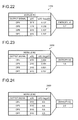
- FIGS. 21 to 25 are diagrams of examples of contents of the entropy table
- FIG. 26 is flowchart of another power index computing procedure of the power index computing apparatus.
- FIG. 27 is a flowchart of one example of an entropy computing process.
- a power index is calculated at a module.
- the power index provides a user with a way to objectively determine a candidate module likely to be wastefully consuming significant power, even if the user does not understand how the circuit is working in detail; thereby improving efficiency in reviewing power consumption of a circuit under design.
- Power consumption at a module includes the power consumed for data communication with another module, the power consumed when clock gating fails, and when unnecessary internal communication (communication between a local memory and a low-level module, for example) are conducted.
- Estimated power consumption obtained by simulation includes these two kinds of power consumption.
- FIG. 1 is a diagram of power consumption at a module.
- a module Ma is a transmitting module that conducts data communication with a module Mb.
- the estimated power consumption is P [mW]
- the data volume conveyed by a data signal (hereinafter, effective data signal) sent from the module Ma to the module Mb is D [bit].
- power consumption at the module Ma includes power consumption caused by failure to perform clock gating and by unnecessary internal communication as well as power consumption for the transmission of data signals to the module Mb.
- measures to improve power consumption at the module Ma are performed, the wasted power resulting from failure to perform clock gating and from unnecessary internal communication is reduced enabling lower power consumption.
- the module Ma can be determined to be efficient or inefficient based on whether the module Ma transmits a data signal whose data volume is comparable to the power consumption P [mW].
- a power index is defined as a quotient of the estimated power consumption P [mW] over the data volume D [bit] of effective data signals.
- a relatively larger power index indicates an inefficient utilization of power while a relatively smaller power index indicates a more efficient utilization of power.
- a user relatively evaluates power indexes of modules of a circuit under design and identifies a candidate module that is a potential contributor to the wasting of power, thereby facilitating efficient and effective power consumption improvements.
- FIG. 2 is a diagram of a hardware configuration of a power index computing apparatus.
- a power index computing apparatus 200 includes a computer 210 , an input device 220 , and an output device 230 and is connectable to a network 240 such as a local area network (LAN), wide area network (WAN), or the Internet via a router or a modem (not shown).
- LAN local area network
- WAN wide area network
- modem not shown
- the computer 210 includes a central processing unit (CPU), a memory, and an interface.
- the CPU controls the entire power index computing apparatus 200 .
- the memory includes a read-only memory (ROM), a random access memory (RAM), a hard drive (HD), an optical disk 211 , and a flash memory.
- ROM read-only memory
- RAM random access memory
- HD hard drive
- optical disk 211 optical disk
- flash memory flash memory
- the memory stores various programs, which are loaded according to an instruction from the CPU.
- the reading/writing of data from and to the HD and the optical disk 211 are controlled by a disk drive. Further, the optical disk 211 and the flash memory are detachable from the computer 210 .
- the interface controls input from input device 220 , output to the output device 230 , and transmission/reception to and from the network 240 .
- the input device 220 includes a keyboard 221 , a mouse 222 , and a scanner 223 .
- the keyboard 221 includes keys to input text, numerals, and various instructions.
- the input device 220 can be a touch panel type device.
- the mouse 222 moves a cursor, determines an area, moves a window, or changes the dimensions for the window.
- the scanner 223 optically scans an image. The scanned image is imported as image data and stored in the memory of the computer 210 .
- the scanner 223 can have an optical character recognition (OCR) function.
- OCR optical character recognition
- the output device 230 includes a display 231 , a printer 232 , and a speaker 233 .
- the display 231 displays a cursor, icons, toolboxes, and data such as documents, images, and function information.
- the speaker 233 outputs sound such as a sound effect, a read-out voice, and the like.
- the printer 232 outputs image date and document data.
- FIG. 3 is a functional diagram of the power index computing apparatus.
- the power index computing apparatus 200 includes an obtaining unit 301 , a first computing unit 302 , a second computing unit 303 , an output unit 304 , a determining unit 305 , and a counting unit 306 .
- the obtaining unit 301 , the first computing unit 302 , the second computing unit 303 , the output unit 304 , the determining unit 305 , and the counting unit 306 that function as a control unit are implemented by, for example, an execution of programs stored in a storage unit such as the ROM, RAM, HD, optical disc 211 , or flash memory shown in FIG. 2 , the programs being executed by the CPU, or may be implemented by the input/output I/F.
- Data output from each of the units (the obtaining unit 301 , the first computing unit 302 , the second computing unit 303 , the output unit 304 , the determining unit 305 , and the counting unit 306 ) is stored in the storage unit.
- a unit at the head of an arrow reads out from the storing unit the data output from a unit at the tail of an arrow and causes the CPU to execute a program for the unit at the head of an arrow.
- the obtaining unit 301 obtains estimated power consumption for a transmitting module in the circuit.
- the estimated power consumption for a transmitting module may be obtained from, for example, an external source (not shown) or by user input, or may be extracted from a database or library (not shown).
- the estimated power consumption may be obtained from a simulation where power consumption at each module is estimated by a conventional estimation method.
- FIG. 4 is a diagram of a power consumption list.
- a power consumption list 400 includes power consumption information items 400 - 1 to 400 -m that indicate estimated power consumption for modules M 1 to Mm in a circuit under design.
- the power consumption information items 400 - 1 to 400 -m respectively correspond to modules M 1 to Mm, and indicate module name and estimated power consumption.
- the power consumption information item 400 -i indicates that the estimated power consumption of a module M 1 is Pi [mW].
- the obtaining unit 301 obtains, for example, the power consumption list 400 (power consumption information items 400 - 1 to 400 -m) as the estimated power consumption of a transmitting module.
- the first computing unit 302 computes the data volume of effective data signals received by a receiving module that communicates with the transmitting module, an effective signal being among the signals transmitted from the transmitting module.
- the data volume of the effective data signals is the data volume of data signals transmitted and received between modules connected through a module interface.
- the data volume of an effective data signal can be expressed by, for example, the number of bits of the effective data signal (data size).
- the second computing unit 303 uses the estimated power consumption obtained by the obtaining unit 301 and the data volume computed by the first computing unit 302 , and computes a power index indicative of the power consumed for transmission of effective data signals with respect to the estimated power consumption.
- the power index is an index for determining whether the workload of the transmitting module is comparable to the estimated power consumption of the transmitting module.
- the power index is computed to determine whether the transmitting module transmits effective data signals whose data volume is comparable to the estimated power consumption.
- the ratio of power consumption for the transmission of effect signals with respect to the estimated power consumption Pi increases.
- the ratio of power consumption for the transmission of effective data signals with respect to the estimated power consumption Pi decreases.
- a power index of a transmitting module may be defined as a quotient of the data volume of effective data signals of a transmitting module over the estimated power consumption.
- a relatively larger power index indicates less wasteful power consumption at the transmitting module.
- a relatively smaller power index indicates more wasteful power consumption at the transmitting module.
- the output unit 304 outputs the computation result obtained by the second computing unit 303 .
- the form of output from the output unit 304 may be screen display at the display 231 , printout at the printer 233 , data output to memory (save), or transmission to an external computer apparatus. Concrete examples of the output from the output unit 304 are described hereinafter.
- the data volume of effective data signals is computed based on, for example, (1) a simulation result that indicates, for each clock cycle, control signals whose values change during the clock cycle, and (2) an interface table that defines, for each module interface, control conditions for data communication to be established between modules.
- the simulation result and the interface table may be obtained by the obtaining unit 301 from an external source, or may be obtained by user input or from a database or library (not shown).
- the simulation result may be an electronic file such as a value change dump (VCD) file in which a clock cycle is associated with control signals whose value has changed during the clock cycle.
- VCD value change dump
- the interface table can be extracted from, for example, a specification describing functions of modules or circuit information for a circuit under design described by hardware description language (VHDL, Verilog, etc.).
- FIG. 5 is a diagram of an example of a simulation result.
- a simulation result 500 includes signal information items 500 - 1 to 500 -n that indicate signals whose values changed while the application was running.
- the signal information items 500 - 1 to 500 -n indicate signals whose values changed during clock cycles 1 to n.
- signal information item 500 -j indicates that at a clock cycle j, a value of a data signal WDATA changed to three and a value of a control signal RECV changed to zero.
- the simulation result 500 indicates, for each clock cycle, only the signals whose values have changed; however, the values of other signals at the previous clock cycle are retained as well, i.e., the simulation result 500 retains the values of all signals at each clock cycle.
- FIG. 6 is a diagram of an interface table.
- an interface table 600 includes, for each module interface C 1 to Ct, module interface information items 600 - 1 to 600 -t that define the passing of data signals between modules.
- the interface information items 600 - 1 to 600 -t include, respectively for the module interfaces C 1 to Ct, information concerning an interface name, a transmitting module name, a receiving module name, a control condition, a data signal, the number of bits, and a priority level.
- the interface name is a name of the module interface C 1 to Ct that connects modules.
- the transmitting module name is the name of a transmitting module.
- the receiving module name is the name of a receiving module.
- the control condition is a condition under which data communication between modules can be established.
- the data signal is an effective data signal to be transmitted and received.
- the number of bits is the data size of a data signal.
- the priority level is an index indicating the importance of a data signal.
- FIG. 7 is a diagram outlining data communication between modules. As depicted in FIG. 7 , a transmitting module M 1 and a receiving module M 2 are connected through a module interface C 1 .
- the interface information item 600 - 1 includes a control condition SEND&RECV under which data communication between the transmitting module M 1 and the receiving module M 2 connected via the module interface C 1 is established.
- This control condition indicates that when control signals SEND and RECV both change, data communication between the transmitting module M 1 and the receiving module M 2 is established.
- the transmitting module M 1 transmits a data signal DATA [ 63 : 0 ] when the control signal SEND changes from 0 to 1.
- the receiving module M 2 receives the data signal DATA [ 63 : 0 ] when a control signal RECV changes from 0 to 1.
- [ 63 : 0 ] defines the number of bits.
- the transmitting module M 1 stops transmission of the data signal DATA [ 63 : 0 ] when the control signal SEND changes from 1 to 0.
- the receiving module M 8 stops reception of the data signal DATA [ 63 : 0 ] when the control signal RECV changes from 1 to 0.
- the priority level of the data signal DATA [ 63 : 0 ] is 1.
- a value of 1 is the minimum priority level.
- a data signal ERROR included in interface information item 600 -k has a priority level of 1000 meaning that the data signal ERROR is 1000 times more important than the data signal DATA [ 63 : 0 ].
- the determining unit 305 determines whether a control signal that has changed during one or multiple clock cycles and a control signal that is defined in a control condition match. For example, the determining unit 305 determines whether control signals match based on the signal information items 500 - 1 to 500 -n depicted in FIG. 5 and the interface information items 600 - 1 to 600 -t.
- control signals identified from the signal information items 500 - 1 to 500 -n match the control signals SEND and RECV that are defined in the control condition SEND&RECV. Sequentially, for each clock cycle 1 to n, it is determined whether respective control signals match.
- the control signal SEND changed from 0 to 1 at clock cycle 1 .
- the determining unit 305 determines that among the control signals defined in the control condition SEND&RECV, only the control signal SEND and the control signal SEND identified from the signal information item 500 - 1 match.
- the control signal RECV has changed from 0 to 1 at clock cycle 2 .
- the determining unit 305 determines that the control signals SEND and RECV, whose signal values have changed at clock cycle 1 and 2 , and the control signals SEND and RECV defined in the control condition SEND&RECV match.
- control signals When multiple control signals are defined in a control condition as described above, information that identifies control signals already determined to match may be stored in the ROM or RAM until all control signals match control signals defined in the control condition (or processes for all clock cycles are completed).
- the counting unit 306 counts how many times the determining unit 305 determines that control signals match; namely, the number of times control conditions are met. In the example above, the counting unit 306 increments the number of times the control condition SEND&RECV of the module interface C 1 is met when the determining unit 305 determines that the control signals SEND and RECV match those defined in the control condition.
- the determining unit 305 determines, for example, for each module interface C 1 to Ct indicated in the interface information 600 - 1 to 600 -t, whether respective control signals at each clock cycle indicated in the signal information 500 - 1 to 500 -n match those defined in a respective control condition.
- the counting unit 306 counts how many times a control condition is met each time the determining unit 305 determines that control signals match.
- the first computing unit 302 computes the data volume of effective data signals of the transmitting module based on a result of the counting by the counting unit 306 and on the number of bits of the effective data signal transmitted and received when a control condition is met.
- the result of the counting by the counting unit 306 indicates how many times control conditions are met.
- the result of the counting is multiplied by the number of bits of the effective data signal transmitted and received when a control condition is met so that for each transmitting module, the total data volume for the effective data signals that have been transmitted to the receiving module from the beginning to the end of the simulation is obtained.
- the data volume of the effective data signals passed through module interfaces C 1 to Ct is obtained for each interface C 1 to Ct.
- the data volume of the effective data signals is obtained based on the number of times effective data has been transmitted (the result of the counting) and on the data size (the number of bits).
- the first computing unit 302 may compute the data volume for each transmitting module based on a priority level of the effective data signal transmitted and received. Thereby, effective data signals with a high priority are weighted, i.e., the data volume of effective data signals is computed based not only on the data volume but also on the priority level of the effective data signal.
- the data volume of effective data signals corresponds to a workload of the transmitting module.
- a data signal ERROR in the interface information 600 -k indicates that failure has occurred in some process, and is a very importance signal.
- the workload is evaluated not only by the number of bits but also by the priority level of the effective data signal.
- a product of a result of the counting performed for each control condition and the number of bits of the effective data signal transmitted and received when a control condition is met is further multiplied by the priority level of the effective data signal; whereby the priority level of the data signal is taken into account and the data volume is obtained.
- the number of times a control condition ERROR.rise of a module interface Ck is met is 1.
- the number of times the control condition is met is 1, the number of bits of an effective data signal is 1, and the priority level is 1000, substitution of these values into equation (3) gives the data volume of effective data signals of the transmitting module M 1 , which is 1000 [bits].
- the control signal ERROR.rise indicates a case when a transmitting module M 7 transmits a data signal ERROR when a control signal ERROR changes from 0 to 1.
- FIG. 8 is a diagram of an effective data signal. As depicted in FIG. 8 , a control condition is CONTROL.rise, a data signal is DATA [ 7 : 0 ], and a priority level is 1.
- a transmitting module transmits the data signal DATA [ 7 : 0 ] whose priority level is 1.
- the number of times a control condition is met is 2, the number of bits of the data signal is 8, and the priority level is 1, substitution of these values into equation (3) gives the data volume of the effective data signals of the transmitting module, which is 16 [bits].
- FIG. 9 is another diagram of an effective data signal. As depicted in FIG. 9 , a data signal DATA[ 7 : 0 ] whose priority level is 1 is transmitted every clock cycle during a period when a control signal CONTROL is 1 (a burst transmission).
- the data volume of the effective data signals of the transmitting module is 40 [bits] when the number of times that a control condition is met is 5, the number of bits of the data signal is 8, and the priority level is 1, and the respective values are substituted into equation (3).
- the determining unit 305 may determine whether a control signal among the multiple control signals and a control signal whose value changed during a clock cycle match.
- the determining unit 305 may determine whether a control signal whose value changed during a clock cycle and, a control signal used for the transmitting module to send an effective data signal or a control signal used for the receiving module to receive the effective data signal match.
- the determining unit 305 determines whether a control signal whose value changed during a cycle clock and, the control signal SEND or the control signal RECV defined in the control condition SEND&RECV match.
- the determining unit 305 completes a determining process once one of the control signals matches a control signal whose value changed. This configuration eliminates the necessity of performing a determining process over multiple clock cycles, thereby reducing the time for the determining process.
- the determining unit 305 may determine whether the value of the effective data signal at the first clock cycle matches the value of the effective data signal at the second clock cycle. Under this configuration, the counting unit 306 may count the number of times the control condition is met when the determining unit 305 determines the values do not match.
- FIG. 10 is another diagram of an effective data signal. As depicted in FIG. 10 , a data signal DATA [ 7 : 0 ] whose priority level is 1 is transmitted during a period when a control signal CONTROL is 1. Symbols A and B in FIG. 10 represent values of the data signal DATA [ 7 : 0 ].
- FIG. 11 is a diagram of output from the first computing unit.
- a list 1100 of effective data volumes includes, respectively corresponding to the transmitting modules, computation results 1100 - 1 to 1100 -m from the first computing unit 302 .
- the data volume of effective data signals for a transmitting module Mi is Di.
- the data volume of effective data signals for each transmitting module is given as a product of the number of times a control condition is met and the number of bits of the data signal (additionally, the priority level of the data signal).
- computation of data volume is not limited hereto.
- the number of bits of the data signal (or a product of the number of bits and the priority level) may be summed each time a control condition is met at each clock cycle; whereby the effective data volume for each transmitting module is obtained.
- the data volume of effective signals for each transmitting module is computed. In other words, it is determined, at each clock cycle 1 to n, whether a control condition for each module interface C 1 to Ct is met.
- the increment x is expressed by the number of bits B of an effective data signal.
- the increment x is expressed by a product of the number of bits B and the priority level I of an effective data signal.
- the obtaining unit 301 may obtain a simulation result that indicates the data volume of effective data signals for each transmitting module.
- the simulation result includes beforehand information concerning the data volume of effective data signals for each transmitting module. Such a simulation result is obtained when a script that monitors the data volume of effective data signals for each transmitting module is written in an execution tool of the simulation.
- a circuit may include a function of monitoring the data volume of effective signals for each transmitting module to obtain such a simulation result. For example, a monitoring circuit that measures the number of times a control condition is met is added to the circuit under design.
- FIG. 12 is a diagram of one example of a monitoring circuit. As depicted in FIG. 12 , a monitoring circuit 1210 that monitors the number of times a control condition of a module interface is met is added to a circuit 1200 that is a subject of a simulation.
- the monitoring circuit 1210 includes a determining circuit 1211 and a counter circuit 1212 .
- the determining circuit 1211 determines whether a control signal whose value changed at a clock cycle and a control signal in the control condition match.
- the counter circuit 1212 counts the number of times the control condition is met when the determining circuit 1211 determines that the control signals match.
- the data volume of effective data signals for each transmitting module is computed based on the number of times the control condition is met as output from the monitoring circuit 1210 .
- the second computing unit 303 computes a power index for each transmitting module based on the simulation result that indicates the data volume of effective data signals for each transmitting module and is obtained by the obtaining unit 301 . In this way, a computation by the first computing unit 302 is omitted and thus the computation of power indices becomes faster.
- the output unit 304 may output a power index for each transmitting module in a circuit under design.
- the output unit 304 outputs a table that correlates and lists names and power indices of transmitting modules. A designer sees the table and can relatively evaluate the power indices of transmitting modules in the circuit under design.
- the output unit 304 may output only the power indices that are more than or equal to a predetermined threshold; namely, the power indices of modules that are likely to contribute significantly to an improvement in power consumption are output.
- a predetermined threshold namely, the power indices of modules that are likely to contribute significantly to an improvement in power consumption are output.
- a user can set the threshold freely by, for example, operating the input device 220 such as the keyboard 221 and the mouse 222 .
- the output unit 304 may correlate and output a power index and an estimated power consumption of a transmitting module.
- the output unit 304 outputs a table that correlates and lists names, indices, and the estimated power consumption of transmitting modules.
- a designer reviews the table and can relatively evaluate the power indices and the estimated power consumption of each transmitting module.
- the output unit 304 may output power indices in ascending order or descending order after a sorting unit (not shown) sorts, in ascending order or descending order, power indices computed by the second computing unit 303 .
- FIG. 13 is a diagram of output results. As depicted in FIG. 13 , an output result list 1300 indicates output result items 1300 - 1 to 1300 - 12 concerning transmitting modules M 1 to M 12 of the circuit under design.
- the output result items 1300 - 1 to 1300 - 12 indicate power indices, effective data volumes, and estimated power consumption concerning transmitting modules M 1 to M 12 .
- a transmitting module M 5 has the highest power consumption 34.29 [mW]
- the power index 1.06 [mW/bit] thereof is the fifth largest.
- the power indices of the transmitting modules M 1 to M 12 can be evaluated relatively and a candidate that is likely to be wasting power can be identified. Since the transmitting module M 10 has the highest power index and the second highest estimated power consumption, it is highly possible that M 10 is wastefully consuming significant power.
- FIG. 14 is a flowchart of computation of a power index. According to the flowchart depicted in FIG. 14 , it is determined whether the obtaining unit 301 has obtained estimated power consumption for a transmitting module of the circuit under design (step S 1401 ).
- step S 1401 Waiting occurs until the estimated power consumption is obtained (step S 1401 : NO).
- step S 1401 YES
- the first computing unit 302 executes an effective data volume computing process to compute the data volume of effective data signals that are transmitted from a transmitting module and are received by a receiving module communicating with the transmitting module (step S 1402 ).
- the second computing unit 303 Based on the estimated power consumption obtained by the obtaining unit 301 and the data volume computed by the first computing unit 302 , the second computing unit 303 computes a power index concerning the power consumed for the transmission of the effective data signals with respect to the estimated power consumption (step S 1403 ).
- the output unit 304 outputs the result from the second computing unit 303 (step S 1404 ), and a series of the process is terminated.
- FIG. 15 is a flowchart of one example of an effective data volume computation process. According to the flowchart depicted in FIG. 15 , it is determined whether the obtaining unit 301 has obtained the simulation result 500 and the interface table 600 (step S 1501 ).
- step S 1501 Waiting occurs until the simulation result 500 and the interface table 600 are obtained (step S 1501 : NO). Once the simulation result 500 and the interface table 600 are obtained (step S 1501 : YES), interface information 600 - 1 to 600 -t for an arbitrary module interface is extracted from the interface table 600 (step S 1502 ).
- Variable j is set to 1 (step S 1503 ) and signal information 500 - 1 to 500 -n for a clock cycle j is extracted from the simulation result 500 (step S 1504 ).
- the determining unit 305 determines whether a control signal whose value has changed at the clock cycle j and a control signal defined in a control condition match (step S 1505 ).
- step S 1505 If the control signals match (step S 1505 : YES), the counting unit 306 counts how many times the control condition defined in the interface information 600 - 1 to 600 -t extracted at step S 1502 is met (step S 1506 ), and j is incremented (step S 1507 ). If the control signals do not match (step S 1505 : NO), the flow goes to step S 1507 .
- step S 1508 It is determined whether j>n (step S 1508 ). If j is not more than n (step S 1508 : NO), the flow returns to step S 1504 and the steps therefrom are repeated. If j is more than n (step S 1508 : YES), it is determined whether there is interface information 600 - 1 to 600 -t that has not yet been extracted (step S 1509 ).
- step S 1509 YES
- the flow returns to step S 1502 and the steps therefrom are repeated.
- step S 1509 the first computing unit 302 computes the data volume of effective data signals for each transmitting module based on the counting result at step S 1506 and the interface information 600 - 1 to 600 -t (step S 1510 ), and the flow goes to step S 1403 depicted in FIG. 14 .
- the determining unit 305 may determine whether all control signals defined and value-changed signals match, or whether one of control signals and a value-changed signal match.
- a process of computing the data volume of effective data signals is explained below with an array variable D [1, 2, . . . , m] that stores effective data volumes of modules M 1 to Mm.
- D array variable
- FIG. 16 is a flowchart of another example of an effective data volume computation process. As depicted in FIG. 16 , it is determined whether the obtaining unit 301 has obtained a simulation result 500 and an interface table 600 (step S 1601 ).
- the interface information 600 - 1 to 600 -t for a module interface Ck is extracted from the interface table 600 (step S 1603 ).
- the signal information 500 - 1 to 500 -n for clock cycle j is extracted from the simulation result 500 (step S 1604 ).
- the determining unit 305 determines whether a control signal whose value has changed at clock cycle j and a control signal defined in a control condition match (step S 1605 ).
- Variable j is incremented (step S 1608 ), and it is determined whether j is more than n (step S 1609 ). If j is not more than n (step S 1609 : NO), the flow returns to step S 1604 and the steps therefrom are repeated. If j is more than n (step S 1609 : YES), k is incremented (step S 1610 ) and it is determined whether k is more than t (step S 1611 ).
- step S 1611 NO
- step S 1611 NO
- step S 1611 YES
- step S 1606 When a control condition is met at contiguous clock cycles j ⁇ 1 and j, it may be determined whether a value of an effective data signal received/transmitted during clock cycle j ⁇ 1 matches a value of an effective data signal received/transmitted during clock cycle j. In this case, the flow goes to step S 1606 when the values do not match and goes to step S 1608 when the values match.
- a power index can be computed.
- the power index enables estimation of wasted power that is not consumed for data communication between modules with respect to estimated power consumption in a module of a circuit under design.
- the power index can be expressed using a data volume of effective data signals transmitted and received between modules.
- the power index is computed based on the data volume of effective data signals for each module M 1 to Mm.
- a power index is computed based on entropy of each module M 1 to Mm.
- FIG. 17 is a diagram of one example of input/output signals of a module.
- a module M is a combinational circuit including logical gates G 1 to G 6 .
- IPa to IPe are input signals to the module M
- OPa to OPd are output signals (output to a destination external to the module M) from the module M.
- a power index of the module M is expressed with entropy that indicates an expected value of a data volume to be output from the module M over an arbitrary simulation period.
- the entropy of the module M is obtained from a transition probability that values of the output signals OPa to OPd transition from 0 to 1 or 1 to 0 during a simulation period.
- Power consumption of the module M increases as the number of transitions of the values of the output signals OPa to OPd during a simulation period increase. Entropy also increases as the number of transitions of the values of the output signals OPa to OPd increases. Consequently, power consumption of the module M increases as entropy of the module M increases.
- a quotient of the estimated power consumption of the module M divided by entropy is computed as a power index.
- the first computing unit 302 computes entropy that is an expected value of a data volume to be output from a module based on a transition probability of each output signal that is output from a module during an arbitrary simulation period.
- the transition probability of an output signal is a probability that the value of the output signal transitions from 1 to 0 or 0 to 1 during an arbitrary simulation period.
- the transition probability can be expressed with an arbitrary probability density function.
- the simulation period can be set freely by a user operating, for example, the input device 200 such as the keyboard 221 or the mouse 222 shown in FIG. 2 . More specifically, the user may designate a clock cycle during a simulation period to set an arbitrary simulation period.
- the second computing unit 303 computes a power index concerning power that is consumed for output to an external destination with respect to the estimated power consumption, based on the estimated power consumption obtained at the obtaining unit 301 and the entropy computed at the first computing unit 302 .
- the power index is, as explained in the first embodiment, an index for determining whether the workload of a module is comparable with the estimated power consumption of the module.
- a module Mi with a larger power index Xi is selected as a subject of improvement for lower power consumption, whereby a significant power reduction can be expected and effective and efficient power improvement can be facilitated.
- entropy of a module is obtained based on a simulation result indicating output signals whose values have changed during a clock cycle and based on an interface table defining output signals from each module.
- the determining unit 305 determines whether an output signal whose value has transitioned during the simulation period and an output signal of a module match.
- FIG. 18 is diagram of another example of a simulation result. As depicted in FIG. 18 , a simulation result 1800 includes signal information items 1800 - 1 to 1800 -n indicating output signals whose values changed while an application was running.
- the signal information 1800 - 1 to 1800 -n includes, for each clock cycle, the name of a signal whose value changed during clock cycle 1 to n. For example, for the signal information item 1800 - 1 , the values of the output signals OP 1 and OP 3 changed at clock cycle 1 .
- FIG. 19 is diagram of another example of an interface table.
- an interface table 1900 includes interface information items 1900 - 1 to 1900 -m defining names of output signals OP 1 to OPx output from modules M 1 to Mm.
- interface information item 1900 - 1 output signals OP 1 , OP 2 and OP 3 output from the module M 1 are defined.
- the determining unit 305 refers to the signal information 1800 -j using the signal name as a clue and identifies an output signal whose value has changed at clock cycle j.
- the determining unit 305 refers to the interface table 1900 using the signal name as a clue and determines whether output signals OP 1 to OPx and the identified output signal match. In this way, it is determined to which module (Ml to Mm) and to which output signal (OP 1 to OPx), the output signal whose value changed at clock cycle j corresponds.
- the counting unit 306 counts the number of transitions of the output signals for each module when the determining unit 305 determines the signals match.
- a counting result table that stores a counting result of the counting unit 306 is explained.
- FIG. 20 is a diagram of an example of the counting result table.
- a counting result table 2000 stores the number of transitions during a simulation period (clock cycle 1 to n) for each output signal OP 1 to OPx output from modules M 1 to Mm. For example, for an output signal OP 1 of the module M 1 , the number of transitions during the simulation period is N 1 .
- the first computing unit 302 computes a transition probability for each output signal based on the counting result of the counting unit 306 .
- Pk ( X ) Nk/T (7)
- the simulation period is defined from clock cycle 1 to clock cycle 10 and the simulation time is defined to be 10.
- the simulation time is defined to be 10.
- entropy table storing a computing result of the first computing unit 302 is explained.
- FIGS. 21 to 25 are diagrams of contents of the entropy table. As depicted in FIGS. 21 to 25 , entropy tables 2100 to 2500 store transition probabilities p(X) for each output signal OP 4 to OP 7 of the module M 2 , intermediate data ⁇ p(X) ⁇ log 2 p(X), and entropy H 2 of M 2 .
- the entropy table 2100 stores entropy H 2 where the number of transitions of OP 7 is especially large, and the number of transitions of OP 4 to OP 6 is one and the number of transitions of OP 7 is nine. H 2 in this case is 1.10.
- the entropy table 2200 stores entropy H 2 where the number of transitions of OP 5 is especially small, and the number of transitions of OP 4 , OP 6 , and OP 7 is nine and the number of transitions of OP 5 is one. H 2 in this case is 0.7.
- the entropy table 2300 stores entropy H 2 where the numbers of transitions of OP 4 to OP 7 vary, and the numbers of transitions of OP 4 to OP 7 are six, two, three, and nine, respectively. H 2 in this case is 1.6.
- the entropy table 2400 stores entropy H 2 where the numbers of transitions of OP 4 to OP 7 are equivalent, and the numbers of transitions of OP 4 to OP 7 are five, respectively.
- H 2 in this case is 2.0.
- the entropy table 2500 stores entropy H 2 where the numbers of transitions of OP 4 to OP 7 are equivalent, and the numbers of transitions of OP 4 to OP 7 are nine, respectively. H 2 in this case is 0.55.
- H 2 takes a maximum value when each output signal OP 4 to OP 7 transitions evenly (see the entropy table 2400 ). On the other hand, H 2 decreases when each output signal OP 4 to OP 7 transitions unevenly (see the entropy table 2100 to 2300 ).
- a power index X 2 of M 2 is a quotient where estimated power consumption P 2 is divided by entropy H 2 .
- the power index X 2 P 2 /2.0
- wasteful power consumption is reduced.
- the power index X 2 P 2 /0.55) and thus wasteful power consumption increases.
- clock cycle 1 to clock cycle n are set beforehand as a simulation period.
- FIG. 26 is flowchart of another power index computing procedure of the power index computing apparatus. As depicted in FIG. 26 , it is determined whether the obtaining unit 301 has obtains power consumption P 1 to Pm for modules M 1 to Mm (the power consumption list 400 , for example) (step S 2601 ).
- step S 2601 Waiting occurs until the estimated power consumption P 1 to Pm is obtained (step S 2601 : NO). Once the estimated power consumption is obtained (step S 2601 : YES), the first computing unit 302 computes entropy H 1 to Hm of the modules M 1 to Mm based on transition probabilities for each output signal from the modules M 1 to Mm at clock cycle 1 to clock cycle n (step S 2602 ).
- the second computing unit 303 Based on the estimated power consumption P 1 to Pm obtained by the obtaining unit 301 and the entropy H 1 to Hm computed by the first computing unit 302 , the second computing unit 303 computes power indices X 1 to Xm concerning power consumed for output with respect to estimated power consumption P 1 to Pm of each module M 1 to Mm (step S 2603 ).
- the output unit 304 outputs the power indices X 1 to Xm of each module M 1 to Mm computed by the second computing unit 303 (step S 2604 ) and the flow is terminated.
- FIG. 27 is a flowchart of one example of an entropy computing process. It is determined whether the obtaining unit 301 has obtained the simulation result 1800 and the interface table 1900 (step S 2701 ).
- step S 2701 Waiting occurs until the simulation result 1800 and the interface table 1900 are obtained (step S 2701 : NO). Once the simulation result and the interface table are obtained (step S 2701 : YES), the counting result table 2000 that stores the numbers of transitions N 1 to Nx of output signals OP 1 to OPx of modules M 1 to Mm is generated (step S 2702 ). At this point, the numbers of transitions N 1 to Nx are initialized and set to 0.
- the signal information 500 -j for clock cycle j is extracted from the simulation result 1800 (step S 2704 ).
- the determining unit 305 determines whether an output signal whose value has changed at clock cycle j and output signals OP 1 to OPx of each module M 1 to Mm match (step S 2705 ).
- the counting unit 306 increments the number of transitions of an output signal that belongs to the counting result table 2000 generated at step S 2702 and that has been determined to match the signal (step S 2706 ).
- step S 2707 After that, j is incremented (step S 2707 ) and it is determined whether j is more than n (step S 2708 ).
- step S 2708 NO
- the flow returns to step S 2704 . If j is more than n (step S 2708 : YES), the first computing unit 302 computes a transition probability for each output signal OP 1 to OPx of each module M 1 to Mm based on the counting result table 2000 and computes entropy H 1 to Hm (step S 2709 ). The flow proceeds to step S 2603 depicted in FIG. 26 .
- a power index can be computed, the power index enabling estimation of power wastefully consumed that is exclusive of the power consumed for output with respect to the estimated power consumption of modules in a circuit under design. More specifically, a power index can be expressed with entropy that indicates an expected value of the volume of data to be output from modules during an arbitrary simulation period.
- the method explained in the present embodiment can be implemented by a computer, such as a personal computer and a workstation, executing a program that is prepared in advance.
- the program is recorded on a computer-readable recording medium such as a hard disk, a flexible disk, a CD-ROM, an MO, and a DVD, and is executed by being read out from the recording medium by a computer.
- the program can be a transmission medium that can be distributed through a network such as the Internet.
- the power index computing apparatus 200 described in the embodiments can be realized by an application specific integrated circuit (ASIC) such as a standard cell or a structured ASIC or a programmable logic device (PLD) such as a field-programmable gate array (FPGA).
- ASIC application specific integrated circuit
- PLD programmable logic device
- FPGA field-programmable gate array
- the functions of the units 301 to 306 of the power index computing apparatus 200 are defined in hardware description language (HDL), which is logically synthesized and applied to the ASIC, the PLD, etc., thereby enabling manufacture of the power index computing apparatus 200 can be manufactured.
- HDL hardware description language
Landscapes
- Engineering & Computer Science (AREA)
- Computer Hardware Design (AREA)
- Physics & Mathematics (AREA)
- Theoretical Computer Science (AREA)
- Microelectronics & Electronic Packaging (AREA)
- Evolutionary Computation (AREA)
- Geometry (AREA)
- General Engineering & Computer Science (AREA)
- General Physics & Mathematics (AREA)
- Design And Manufacture Of Integrated Circuits (AREA)
Abstract
Description
Xi=Pi/Di (1)
Di=F×B (2)
Di=F×B×I (3)
x=B (4)
x=B×I (5)
Xi=Pi/Hi (6)
Pk(X)=Nk/T (7)
H1=−p 1(X)·log2(p 1(X))−p 2(X)·log2(p 2(X))−p 3(X)·log2(p 3(X)).
Claims (16)
Applications Claiming Priority (4)
| Application Number | Priority Date | Filing Date | Title |
|---|---|---|---|
| JP2007-312461 | 2007-12-03 | ||
| JP2007312461 | 2007-12-03 | ||
| JP2008-168981 | 2008-06-27 | ||
| JP2008168981A JP5374937B2 (en) | 2007-12-03 | 2008-06-27 | Power index calculation program, power index calculation device, and power index calculation method |
Publications (2)
| Publication Number | Publication Date |
|---|---|
| US20090157375A1 US20090157375A1 (en) | 2009-06-18 |
| US8095353B2 true US8095353B2 (en) | 2012-01-10 |
Family
ID=40754392
Family Applications (1)
| Application Number | Title | Priority Date | Filing Date |
|---|---|---|---|
| US12/325,206 Expired - Fee Related US8095353B2 (en) | 2007-12-03 | 2008-11-30 | Power index computing apparatus, method of computing power index, and computer product |
Country Status (1)
| Country | Link |
|---|---|
| US (1) | US8095353B2 (en) |
Families Citing this family (6)
| Publication number | Priority date | Publication date | Assignee | Title |
|---|---|---|---|---|
| US8825464B2 (en) * | 2008-09-02 | 2014-09-02 | Oracle America, Inc. | Method and apparatus for parallelization of sequential power simulation |
| JP2011237989A (en) * | 2010-05-10 | 2011-11-24 | Toshiba Corp | Apparatus for designing semiconductor integrated circuit, and method and program for designing the same |
| US9430599B2 (en) * | 2014-02-18 | 2016-08-30 | Optima Design Automation Ltd | Determining soft error infliction probability |
| GB2542215B (en) * | 2016-01-18 | 2018-04-11 | Imagination Tech Ltd | Dynamic power measurement using a formal verification tool |
| US10949588B1 (en) * | 2016-11-10 | 2021-03-16 | Synopsys, Inc. | High speed, low hardware footprint waveform |
| JP2021022000A (en) * | 2019-07-24 | 2021-02-18 | 京セラドキュメントソリューションズ株式会社 | Print system |
Citations (17)
| Publication number | Priority date | Publication date | Assignee | Title |
|---|---|---|---|---|
| JP2001056827A (en) | 1999-08-18 | 2001-02-27 | Matsushita Electric Ind Co Ltd | Integrated circuit device design method |
| US6204707B1 (en) * | 1998-08-26 | 2001-03-20 | Kabushiki Kaisha Toshiba | Flip-flop circuit with clock signal control function and clock control circuit |
| US20020126565A1 (en) * | 2001-01-23 | 2002-09-12 | Mitsubishi Denki Kabushiki Kaisha | Semiconductor integrated circuit device with internal clock generating circuit |
| US20020133241A1 (en) * | 2001-02-23 | 2002-09-19 | Yoshitaka Takahashi | Logic circuit module having power consumption control interface and a recording medium storing the module |
| US6480815B1 (en) * | 1996-10-29 | 2002-11-12 | Synopsys, Inc. | Path dependent power modeling |
| US20040054976A1 (en) | 1999-08-18 | 2004-03-18 | Matsushita Electric Industrial Co., Ltd. | Method of designing integrated circuit device and database |
| JP2004228417A (en) | 2003-01-24 | 2004-08-12 | Renesas Technology Corp | Semiconductor integrated circuit apparatus |
| US20050040873A1 (en) * | 2003-08-20 | 2005-02-24 | Tooru Wada | Semiconductor integrated circuit |
| US6992948B2 (en) * | 2001-03-22 | 2006-01-31 | Matsushita Electric Industrial Co., Ltd. | Memory device having address generating circuit using phase adjustment by sampling divided clock to generate address signal of several bits having one bit changed in sequential order |
| US20060082400A1 (en) * | 2004-10-19 | 2006-04-20 | Matsushita Electric Industrial Co., Ltd. | Register circuit, and synchronous integrated circuit that includes a register circuit |
| US7076405B1 (en) * | 1999-09-17 | 2006-07-11 | Kabushiki Kaisha Toshiba | Method for estimating power consumption and noise levels of an integrated circuit, and computer-readable recording medium storing a program for estimating power consumption and noise levels of an integrated circuit |
| JP2006277332A (en) | 2005-03-29 | 2006-10-12 | Seiko Epson Corp | Integrated circuit device, microcomputer and electronic device |
| US20060248354A1 (en) * | 2003-05-27 | 2006-11-02 | Koninklijke Philips Electronics N.V. | Monitoring and controlling power consumption |
| US20060256066A1 (en) * | 2002-06-10 | 2006-11-16 | Seung-Hwan Moon | Shift register, liquid crystal display device having the shift register and method of driving scan lines using the same |
| WO2007037017A1 (en) | 2005-09-29 | 2007-04-05 | Fujitsu Limited | Consumed power analyzing method, and consumed power analyzing device |
| US20080162071A1 (en) * | 2006-12-27 | 2008-07-03 | Ashley Miles Stevens | Communication of a diagnostic signal and a functional signal by an integrated circuit |
| US7580824B1 (en) * | 2005-12-21 | 2009-08-25 | Altera Corporation | Apparatus and methods for modeling power characteristics of electronic circuitry |
-
2008
- 2008-11-30 US US12/325,206 patent/US8095353B2/en not_active Expired - Fee Related
Patent Citations (17)
| Publication number | Priority date | Publication date | Assignee | Title |
|---|---|---|---|---|
| US6480815B1 (en) * | 1996-10-29 | 2002-11-12 | Synopsys, Inc. | Path dependent power modeling |
| US6204707B1 (en) * | 1998-08-26 | 2001-03-20 | Kabushiki Kaisha Toshiba | Flip-flop circuit with clock signal control function and clock control circuit |
| JP2001056827A (en) | 1999-08-18 | 2001-02-27 | Matsushita Electric Ind Co Ltd | Integrated circuit device design method |
| US20040054976A1 (en) | 1999-08-18 | 2004-03-18 | Matsushita Electric Industrial Co., Ltd. | Method of designing integrated circuit device and database |
| US7076405B1 (en) * | 1999-09-17 | 2006-07-11 | Kabushiki Kaisha Toshiba | Method for estimating power consumption and noise levels of an integrated circuit, and computer-readable recording medium storing a program for estimating power consumption and noise levels of an integrated circuit |
| US20020126565A1 (en) * | 2001-01-23 | 2002-09-12 | Mitsubishi Denki Kabushiki Kaisha | Semiconductor integrated circuit device with internal clock generating circuit |
| US20020133241A1 (en) * | 2001-02-23 | 2002-09-19 | Yoshitaka Takahashi | Logic circuit module having power consumption control interface and a recording medium storing the module |
| US6992948B2 (en) * | 2001-03-22 | 2006-01-31 | Matsushita Electric Industrial Co., Ltd. | Memory device having address generating circuit using phase adjustment by sampling divided clock to generate address signal of several bits having one bit changed in sequential order |
| US20060256066A1 (en) * | 2002-06-10 | 2006-11-16 | Seung-Hwan Moon | Shift register, liquid crystal display device having the shift register and method of driving scan lines using the same |
| JP2004228417A (en) | 2003-01-24 | 2004-08-12 | Renesas Technology Corp | Semiconductor integrated circuit apparatus |
| US20060248354A1 (en) * | 2003-05-27 | 2006-11-02 | Koninklijke Philips Electronics N.V. | Monitoring and controlling power consumption |
| US20050040873A1 (en) * | 2003-08-20 | 2005-02-24 | Tooru Wada | Semiconductor integrated circuit |
| US20060082400A1 (en) * | 2004-10-19 | 2006-04-20 | Matsushita Electric Industrial Co., Ltd. | Register circuit, and synchronous integrated circuit that includes a register circuit |
| JP2006277332A (en) | 2005-03-29 | 2006-10-12 | Seiko Epson Corp | Integrated circuit device, microcomputer and electronic device |
| WO2007037017A1 (en) | 2005-09-29 | 2007-04-05 | Fujitsu Limited | Consumed power analyzing method, and consumed power analyzing device |
| US7580824B1 (en) * | 2005-12-21 | 2009-08-25 | Altera Corporation | Apparatus and methods for modeling power characteristics of electronic circuitry |
| US20080162071A1 (en) * | 2006-12-27 | 2008-07-03 | Ashley Miles Stevens | Communication of a diagnostic signal and a functional signal by an integrated circuit |
Also Published As
| Publication number | Publication date |
|---|---|
| US20090157375A1 (en) | 2009-06-18 |
Similar Documents
| Publication | Publication Date | Title |
|---|---|---|
| US8095353B2 (en) | Power index computing apparatus, method of computing power index, and computer product | |
| CN101877017B (en) | Efficient exhaustive path-based static timing analysis using a fast estimation technique | |
| US20090282377A1 (en) | Verification support apparatus, verification support method, and computer product | |
| US8468478B2 (en) | Methods for measurement and prediction of hold-time and exceeding hold time limits due to cells with tied input pins | |
| US20050172250A1 (en) | System and method for providing distributed static timing analysis with merged results | |
| US6745371B2 (en) | Low Vt transistor substitution in a semiconductor device | |
| US7464015B2 (en) | Method and apparatus for supporting verification, and computer product | |
| US7546559B2 (en) | Method of optimization of clock gating in integrated circuit designs | |
| WO2004094995A2 (en) | Hierarchical evaluation of cells | |
| Gupta et al. | Analytical models for RTL power estimation of combinational and sequential circuits | |
| US20100050144A1 (en) | System and method for employing signoff-quality timing analysis information to reduce leakage power in an electronic circuit and electronic design automation tool incorporating the same | |
| US8074186B2 (en) | Leakage current analyzing apparatus, leakage current analyzing method, and computer product | |
| CN115454398A (en) | Floating point calculation precision analysis method and system of C language program verifier | |
| US8024685B2 (en) | Delay analysis support apparatus, delay analysis support method and computer product | |
| US20140040845A1 (en) | System and method for employing side transition times from signoff-quality timing analysis information to reduce leakage power in an electronic circuit and an electronic design automation tool incorporating the same | |
| US8942968B2 (en) | Analysis support computer product, apparatus, and method | |
| US20060129957A1 (en) | Method and computer program product for register transfer level power estimation in chip design | |
| US20050005199A1 (en) | System and method for analyzing noise | |
| JP5262442B2 (en) | Design support program, design support apparatus, and design support method | |
| US7222039B2 (en) | Estimation of average-case activity for digital state machines | |
| US20230418324A1 (en) | Method for programming an fpga | |
| US20080195985A1 (en) | Apparatus, method, and computer product for estimating power consumption of LSI | |
| CN101395484A (en) | Efficient calculation of transition numbers and estimation of power dissipation in continuous scan tests | |
| JP5277781B2 (en) | Power consumption estimation program, computer-readable recording medium recording the program, power consumption estimation device, and power consumption estimation method | |
| US20060282803A1 (en) | Estimation of average-case activity for digital circuits |
Legal Events
| Date | Code | Title | Description |
|---|---|---|---|
| AS | Assignment |
Owner name: FUJITSU LIMITED, JAPAN Free format text: ASSIGNMENT OF ASSIGNORS INTEREST;ASSIGNORS:YAMAMOTO, TATSUYA;TAMIYA, YUTAKA;REEL/FRAME:021900/0862 Effective date: 20080911 |
|
| FEPP | Fee payment procedure |
Free format text: PAYOR NUMBER ASSIGNED (ORIGINAL EVENT CODE: ASPN); ENTITY STATUS OF PATENT OWNER: LARGE ENTITY |
|
| STCF | Information on status: patent grant |
Free format text: PATENTED CASE |
|
| FPAY | Fee payment |
Year of fee payment: 4 |
|
| FEPP | Fee payment procedure |
Free format text: MAINTENANCE FEE REMINDER MAILED (ORIGINAL EVENT CODE: REM.); ENTITY STATUS OF PATENT OWNER: LARGE ENTITY |
|
| LAPS | Lapse for failure to pay maintenance fees |
Free format text: PATENT EXPIRED FOR FAILURE TO PAY MAINTENANCE FEES (ORIGINAL EVENT CODE: EXP.); ENTITY STATUS OF PATENT OWNER: LARGE ENTITY |
|
| STCH | Information on status: patent discontinuation |
Free format text: PATENT EXPIRED DUE TO NONPAYMENT OF MAINTENANCE FEES UNDER 37 CFR 1.362 |
|
| FP | Lapsed due to failure to pay maintenance fee |
Effective date: 20200110 |