US8093822B2 - LED driver and control method thereof - Google Patents
LED driver and control method thereof Download PDFInfo
- Publication number
- US8093822B2 US8093822B2 US12/216,837 US21683708A US8093822B2 US 8093822 B2 US8093822 B2 US 8093822B2 US 21683708 A US21683708 A US 21683708A US 8093822 B2 US8093822 B2 US 8093822B2
- Authority
- US
- United States
- Prior art keywords
- signal
- current
- led
- generate
- led lighting
- Prior art date
- Legal status (The legal status is an assumption and is not a legal conclusion. Google has not performed a legal analysis and makes no representation as to the accuracy of the status listed.)
- Active, expires
Links
Images


Classifications
-
- H—ELECTRICITY
- H05—ELECTRIC TECHNIQUES NOT OTHERWISE PROVIDED FOR
- H05B—ELECTRIC HEATING; ELECTRIC LIGHT SOURCES NOT OTHERWISE PROVIDED FOR; CIRCUIT ARRANGEMENTS FOR ELECTRIC LIGHT SOURCES, IN GENERAL
- H05B45/00—Circuit arrangements for operating light-emitting diodes [LED]
- H05B45/30—Driver circuits
- H05B45/37—Converter circuits
- H05B45/3725—Switched mode power supply [SMPS]
-
- H—ELECTRICITY
- H05—ELECTRIC TECHNIQUES NOT OTHERWISE PROVIDED FOR
- H05B—ELECTRIC HEATING; ELECTRIC LIGHT SOURCES NOT OTHERWISE PROVIDED FOR; CIRCUIT ARRANGEMENTS FOR ELECTRIC LIGHT SOURCES, IN GENERAL
- H05B45/00—Circuit arrangements for operating light-emitting diodes [LED]
- H05B45/20—Controlling the colour of the light
- H05B45/24—Controlling the colour of the light using electrical feedback from LEDs or from LED modules
-
- H—ELECTRICITY
- H05—ELECTRIC TECHNIQUES NOT OTHERWISE PROVIDED FOR
- H05B—ELECTRIC HEATING; ELECTRIC LIGHT SOURCES NOT OTHERWISE PROVIDED FOR; CIRCUIT ARRANGEMENTS FOR ELECTRIC LIGHT SOURCES, IN GENERAL
- H05B45/00—Circuit arrangements for operating light-emitting diodes [LED]
- H05B45/30—Driver circuits
- H05B45/37—Converter circuits
- H05B45/3725—Switched mode power supply [SMPS]
- H05B45/375—Switched mode power supply [SMPS] using buck topology
-
- H—ELECTRICITY
- H05—ELECTRIC TECHNIQUES NOT OTHERWISE PROVIDED FOR
- H05B—ELECTRIC HEATING; ELECTRIC LIGHT SOURCES NOT OTHERWISE PROVIDED FOR; CIRCUIT ARRANGEMENTS FOR ELECTRIC LIGHT SOURCES, IN GENERAL
- H05B45/00—Circuit arrangements for operating light-emitting diodes [LED]
- H05B45/30—Driver circuits
- H05B45/37—Converter circuits
- H05B45/3725—Switched mode power supply [SMPS]
- H05B45/38—Switched mode power supply [SMPS] using boost topology
-
- H—ELECTRICITY
- H05—ELECTRIC TECHNIQUES NOT OTHERWISE PROVIDED FOR
- H05B—ELECTRIC HEATING; ELECTRIC LIGHT SOURCES NOT OTHERWISE PROVIDED FOR; CIRCUIT ARRANGEMENTS FOR ELECTRIC LIGHT SOURCES, IN GENERAL
- H05B45/00—Circuit arrangements for operating light-emitting diodes [LED]
- H05B45/30—Driver circuits
- H05B45/37—Converter circuits
- H05B45/3725—Switched mode power supply [SMPS]
- H05B45/385—Switched mode power supply [SMPS] using flyback topology
-
- Y—GENERAL TAGGING OF NEW TECHNOLOGICAL DEVELOPMENTS; GENERAL TAGGING OF CROSS-SECTIONAL TECHNOLOGIES SPANNING OVER SEVERAL SECTIONS OF THE IPC; TECHNICAL SUBJECTS COVERED BY FORMER USPC CROSS-REFERENCE ART COLLECTIONS [XRACs] AND DIGESTS
- Y02—TECHNOLOGIES OR APPLICATIONS FOR MITIGATION OR ADAPTATION AGAINST CLIMATE CHANGE
- Y02B—CLIMATE CHANGE MITIGATION TECHNOLOGIES RELATED TO BUILDINGS, e.g. HOUSING, HOUSE APPLIANCES OR RELATED END-USER APPLICATIONS
- Y02B20/00—Energy efficient lighting technologies, e.g. halogen lamps or gas discharge lamps
- Y02B20/30—Semiconductor lamps, e.g. solid state lamps [SSL] light emitting diodes [LED] or organic LED [OLED]
Definitions
- the present invention is related generally to a light emitting diode (LED) driver and, more particularly, to a circuit and method for constant average current regulation of an LED lighting apparatus.
- LED light emitting diode
- LED lighting control There are two typical methods for LED lighting control. One of them is constant average current modulation, such as the controller chip RT9271 (http://www.richtek.com/www/Docs/DS9271-13.pdf) of Richtek Technology Corporation, and the other is constant peak current modulation, such as the controller chip AMC7150 (http://www.addmtek.com/Datasheet/DD034-AMC7150%20_A.pdf) of ADDtek Corporation and the controller chip HV9910 (http://www.supertex.com/pdf/datasheets/HV9910.pdf) of Supertex Incorporation.
- constant average current modulation such as the controller chip RT9271 (http://www.richtek.com/www/Docs/DS9271-13.pdf) of Richtek Technology Corporation
- constant peak current modulation such as the controller chip AMC7150 (http://www.addmtek.com/Datasheet/DD034-AMC7150%20_A.pdf) of ADDtek Corporation and the controller chip HV9910
- FIG. 1 is an application circuit given in the data sheet of RT9271.
- a power switch (not shown) is connected between a switch pin LX and a ground pin GND for being switched in response to a pulse width modulation (PWM) signal to regulate the current I LED supplied to light emitting diodes LED 1 -LED 3 .
- PWM pulse width modulation
- This control scheme requires a rectifier diode D and an output capacitor Cout for filtering so as to provide a stable average current for the light emitting diodes LED 1 -LED 3 .
- the output capacitor Cout requires a greater capacitance and thus this prior art requires a larger and more costly component for the capacitor.
- the output capacitor Cout will need to sustain a high voltage, which also causes this prior art to require a larger and expensive component.
- FIG. 2 is an application circuit given in the data sheet of AMC7150.
- a power switch (not shown) is connected between a current sense pin Is and an output pin OUT for being switched in response to a modulation signal so as to regulate the current I LED supplied to light emitting diodes LED 1 and LED 2 .
- FIG. 3 is an application circuit given in the data sheet of HV9910.
- An output pin Gate of a controller chip 14 provides a modulation signal to switch a power switch SW, so as to regulate the current I LED supplied to light emitting diodes LED 1 and LED 2 .
- the output capacitor Cout in the circuit of FIG. 3 may be removed without destroying the control.
- a peak current control scheme which sets a threshold I PK as the peak current.
- a control signal is triggered to decrease the current I LED .
- Ton the time period where the power switch SW is on
- the current I LED increases, as shown by the time period Ton of the waveform 16 in FIG. 4 .
- the power switch SW is turned off and the current I LED begins decreasing, as shown in the time period Toff of FIG. 4 .
- FIGS. 2 and 3 can provide stable LED current without the need of large output capacitor Cout as required by the control circuit of FIG. 1 , they are inherently disadvantageous to some applications due to the constant peak current control.
- the slope and valley value of the LED current vary accordingly and thus it causes variation of the average LED current.
- the Vin dependent average LED current variation is especially worse in Boost mode or Buck-Boost mode configurations.
- FIG. 5 depicts a boost LED driver and FIG. 6 shows the variation of the inductor current IL of this driver as a consequence of the variation of the input voltage Vin.
- the inductor current IL flows from the power input Vin toward the ground terminal GND through the power switch SW.
- the inductor current IL redirects to the light emitting diodes LED 1 and LED 2 .
- the inductor current IL increases at a higher speed, and thus the power switch SW will have a shorter on time Ton 1 for the current threshold I PK to be reached, as shown by the waveform 18 in FIG. 6 .
- the inductor current IL increases slower, and longer on time Ton 2 is required for the power switch SW, so as for the peak current I PK to be reached, as shown by the waveform 20 in FIG.
- An object of the present invention is to provide an LED driver and control method for real constant average current regulation of an LED lighting apparatus.
- Another object of the present invention is to provide an LED driver and control method which eliminate the need of an output capacitor.
- Yet another object of the present invention is to provide an LED driver and control method which eliminate the need of a rectifier diode in most applications.
- Still another object of the present invention is to provide a size-reduced and lower cost LED driver.
- Still yet another object of the present invention is to provide an LED driver and control method applicable to various circuit configurations.
- an LED driver extracts the LED lighting current information from an LED path to produce a first signal including an AC component and a DC component, and extracts the DC component information of the first signal to produce a second signal to regulate an average of the LED lighting current.
- the power stage connected to the LED path is simplified by eliminating the output capacitor.
- a feedback loop uses a filter to acquire a difference between the average of the LED lighting current and a setting value.
- Yet another aspect of the present invention is to directly control the ripple and DC level of the LED lighting current.
- control signal may have constant on-time or off-time.
- control signal may have constant switching frequency
- FIG. 1 is an application circuit given in the data sheet of RT9271;
- FIG. 2 is an application circuit given in the data sheet of AMC7150
- FIG. 3 is an application circuit given in the data sheet of HV9910
- FIG. 4 illustrates the operational principle of the control circuits of FIGS. 2 and 3 ;
- FIG. 5 depicts a boost LED driver
- FIG. 6 shows the inductor current of the circuit of FIG. 5 along the variation of the input voltage
- FIG. 7 is a non-inverting LED driver according to the present invention.
- FIG. 8 is an inverting LED driver according to the present invention.
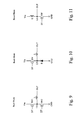
- FIG. 9 shows a simplified power stage of a synchronous buck configuration
- FIG. 10 shows a simplified power stage of an asynchronous buck configuration
- FIG. 11 shows a simplified power stage of a boost configuration
- FIG. 12 shows a simplified power stage of a synchronous buck-boost configuration
- FIG. 13 shows a simplified power stage of an asynchronous buck-boost configuration
- FIG. 14 shows a simplified power stage of a flyback configuration
- FIG. 15 shows a simplified power stage of an inverting configuration
- FIG. 16 is a pulse width modulation (PWM) regulation loop
- FIG. 17 is a hysteresis mode regulation loop
- FIG. 18 is a delay mode regulation loop
- FIG. 19 is a hysteresis mode regulation loop in different structure from that in FIG. 17 ;
- FIG. 20 is the first embodiment of the error signal generator
- FIG. 21 is the second embodiment of the error signal generator
- FIG. 22 is the third embodiment of the error signal generator
- FIG. 23 is the first embodiment of the current sensor
- FIG. 24 is the second embodiment of the current sensor
- FIG. 25 is the third embodiment of the current sensor
- FIG. 26 is a frequency regulation loop
- FIG. 27 is a frequency to voltage converter
- FIG. 28 is a frequency regulation loop
- FIG. 29 is the first embodiment of the signal modulator.
- FIG. 30 is the second embodiment of the signal modulator.
- FIG. 7 shows an LED driver having a non-inverting configuration according to the present invention, which provides an LED lighting current I LED to an LED path built between nodes A and B, with light emitting diodes LED 1 -LED 3 thereon.
- the node A is connected to a simplified power stage 30 of the LED driver and the node B is connected to a current-sensor 32 , and to a ground terminal GND.
- a feedback loop provides an error signal Ve to a controller 40 of the LED driver, so as to determine a control signal DT to operate the simplified output stage 30 , and thus the simplified power stage 30 regulates the LED lighting current I LED according to the control signal DT.
- the current sensor 32 monitors the LED lighting current I LED to generate a current sense signal Si; a low-pass filter 34 filters the current sense signal Si to generate a DC level signal Sidc that represents the average of the LED lighting current I LED ; a reference signal generator 36 provides a preset reference signal Sr that represents a preset value for the average of the LED lighting current I LED ; and an error signal generator 38 generates the error signal Ve according to the difference between the signals Sidc and Sr.
- the DC level signal Sidc is higher than the reference signal Sr, it means that the average of the LED lighting current I LED is higher than the preset value.
- the controller 40 modifies DT for controlling the magnitude of the LED lighting current LED according to the error signal Ve so as to regulate the average of the LED lighting current I LED at the preset value.
- the simplified power stage 30 does not require a large filtering capacitor at its output terminal OUT, and thus the size and cost thereof are reduced.
- the low-pass filter 34 in some applications, may need a capacitor to filter the current sense signal Si, it adequates merely a small low-voltage one, and as compared with the output capacitor Cout of FIG. 1 , the cost of such a small capacitor can be almost ignored.
- the low-pass filter 34 may be moved to the position between the error signal generator 38 and the controller 40 .
- the comparison of the current sense signal Si and the reference signal Sr by the error signal generator 38 is done first, and the output of the error signal generator 38 is filtered by the low-pass filter 34 next to generate the final error signal Ve.
- an error signal generator with very low bandwidth may be employed as the element 38 which thus simultaneously includes the functions of a low-pass filter.
- the current sensor 32 may sense the LED lighting current I LED at a position other than the node B, such as the node A, or any part of the LED path, or any part out of the LED path at which the magnitude information of the LED lighting current I LED can be extracted.
- FIG. 8 shows an LED driver having an inverting configuration according to the present invention, in which the output of the simplified power stage 30 is a current-sinking terminal, and the node B is connected to a ground terminal GND or any power sourcing node, such as Vin.
- the light emitting diodes current I LED flowing therethrough is opposite in direction to that of the embodiment shown in FIG. 7 , while the rest of the configuration and principle are identical to those of the embodiment shown in FIG. 7 .
- the low-pass filter 34 can be moved to the position between the error signal generator 38 and the controller 40 , or be included in an error signal generator with low bandwidth.
- Each simplified switching mode power stage includes at least one power switch, switching according to the control signal DT to regulate the LED lighting current I LED .
- FIGS. 9 to 14 provide several embodiments applicable to the simplified power stage 30 of FIG. 7 .
- FIG. 9 shows a simplified power stage configured in synchronous buck mode, in which power switches SW 1 and SW 2 are serially connected between the power input Vin and ground terminal GND, an inductor L is connected between the phase node LX and output terminal OUT, and the control signal DT is a PWM signal or a variant frequency modulation (VFM) signal to switch the power switches SW 1 and SW 2 .
- VFM variant frequency modulation
- FIG. 10 shows a simplified power stage configured in asynchronous buck mode, in which a power switch SW and a diode D are serially connected between the power input Vin and ground terminal GND, an inductor L is connected between the phase node LX and output terminal OUT, and the control signal DT is a PWM signal or a VFM signal to switch the power switch SW.
- FIG. 11 shows a simplified power stage configured in boost mode, in which an inductor L and a power switch SW are serially connected between the power input Vin and ground terminal GND, the output OUT is directly drawn out from the phase node LX, and the control signal DT is a PWM signal or a VFM signal to switch the power switch SW.
- an asynchronous boost mode power stage includes a rectifier diode between the phase node LX and output terminal OUT.
- the output terminal OUT is connected to the light emitting diodes, the light emitting diodes can act as the rectifier so as to save a diode at the output terminal OUT.
- FIG. 12 shows a simplified power stage configured in synchronous buck-boost mode, in which power switches SW 1 and SW 2 are serially connected between the power input Vin and ground terminal GND, an inductor L is connected between the phase node LX and output terminal OUT, another power switch SW 3 is connected between the output terminal OUT and ground GND, and the control signal DT is a PWM signal or a VFM signal to switch the power switches SW 1 , SW 2 and SW 3 .
- FIG. 13 shows a simplified power stage configured in asynchronous buck-boost mode, in which a power switch SW 1 and a diode D are serially connected between the power input Vin and ground terminal GND, an inductor L is connected between the phase node LX and output terminal OUT, another power switch SW 2 is connected between the output terminal OUT and ground terminal GND, and the control signal DT is a PWM signal or a VFM signal to switch the power switches SW 1 and SW 2 .
- a flyback mode power stage includes a rectifier diode between the secondary coil TXs and the output terminal OUT.
- the output terminal OUT is connected to the light emitting diodes, the light emitting diodes can act as the rectifier so as to save a diode at the output terminal OUT.
- FIG. 15 shows an embodiment applicable to the simplified power stage 30 of FIG. 8 , in which a power switch SW and an inductor L are serially connected between the power input Vin and ground terminal GND, the output terminal OUT directly sinks the LED current to the phase node LX, and the control signal DT is a PWM signal or a VFM signal to switch the power switch SW.
- an inverting mode power stage includes a power switch or a rectifier diode between the phase node LX and the output terminal OUT.
- the output terminal OUT since the output terminal OUT is connected to the light emitting diodes, it saves a power switch or a diode at the output terminal OUT.
- the LED driver of the present invention can be applicable to almost all types of power stages.
- FIGS. 16 to 19 provide several embodiments for the controller 40 of FIG. 7 or FIG. 8 .
- this embodiment employs a comparator COMP to compare the error signal Ve and a signal Ss to generate a PWM signal DT to adjust the level of the LED lighting current I LED and thereby to keep the average value of the LED lighting current I LED constant.
- the signal Ss is in saw-tooth-like waveform, which can be the load current (the LED lighting current in this case) feedback signal, or an oscillating signal generated by a ramping oscillator. If the signal Ss is a load current feedback signal, it includes both the DC and AC components of the LED lighting current I LED , which is provided by the LED current sensor circuit.
- the current sensor circuit can be identical or similar to the current sensor 32 of FIG. 7 and FIG. 8 , and the position where it senses the current can be the same as or different from that of the current sensor 32 .
- the PWM waveform diagram is illustrated in the right part of FIG. 16 . Similar to the general PWM control, the on time Ton of the PWM signal DT is during the time period that the signal Ss is lower than the signal Ve, and the off time Toff of the PWM signal DT is during the time period that the signal Ss is higher than the signal Ve.
- the on-time Ton or the off-time Toff of the PWM signal DT determines the ripple and DC level of the LED lighting current I LED .
- the error signal Ve When the average value of the LED lighting current I LED changes, the error signal Ve will change accordingly, and the on-time Ton or the off-time Toff of the PWM signal DT will also change.
- the change of Ton and Toff will adjust the DC level of the LED lighting current I LED back to the preset level, thereby the average value of the LED lighting current I LED is kept constant.
- FIG. 17 provides a hysteresis mode regulation loop and a waveform diagram thereof.
- the signal Ss is the LED lighting current feedback signal, which is provided by the LED current sensor circuit.
- the equation EQ-1 is merely for an example and other modulation functions are also feasible.
- a hysteresis comparator HYSCOMP has a preset hysteresis parameter Hys to determine another current limit setting CL ⁇ Hys.
- the hysteresis parameter Hys represents the hysteresis gap width.
- the signal Ss is compared with the current limit settings CL and CL ⁇ Hys to generate the control signal DT.
- the time period that the signal Ss rises from CL ⁇ Hys to CL is the on-time Ton of the control signal DT, and the time period that the signal Ss descends from CL to CL ⁇ Hys is the off-time Toff of the control signal DT.
- the error signal Ve varies accordingly and the final current limit level CL also varies accordingly so as to modulate the peak and valley levels of the LED lighting current LED, thereby keeping the average value of the LED lighting current LED constant.
- the upper and lower limits for the signal Ss in the hysteresis mode regulation control may be set in various other ways. For instance, two alternative embodiments are provided at the lower part of FIG. 17 . In the left waveform diagram, the current limits are set as CL+Hys and CL, respectively, and in the right waveform diagram, the current limits are set as CL+Hys ⁇ [n/(m+n)] and CL ⁇ Hys ⁇ [m/(m+n)], respectively, where m and n are coefficients for modulating the center value of the hysteresis gap.
- FIG. 18 provides a delay mode regulation loop and a waveform diagram thereof, in which a signal modulator 42 generates a final current limit level CL according to the error signal Ve and a current limit setting CLo, and a delay comparator TDCOMP compares the signals CL and Ss to generate the control signal DT.
- the signal Ss is the LED lighting current feedback signal, which is provided by the LED current sensor circuit.
- the modulation function of the signal modulator 42 for example may be the equation EQ-1, or others.
- the delay times Td 1 and Td 2 are determined by the parameters of the delay comparator TDCOMP. Since the final current limit level CL varies along with the variation of the error signal Ve, when the average of the LED lighting current I LED varies, the final current limit level CL varies accordingly to correspondingly modulate the DC level of the LED lighting current I LED , thereby keeping the average value of the LED lighting current I LED constant. In some embodiments, one of the delay times Td 1 and Td 2 can be as to realize a constant off-time mode or a constant on-time mode.
- FIG. 19 provides another embodiment for the controller 40 , in which a signal modulator 42 generates two final current limit levels VCL 1 and VCL 2 according to a current limit setting CLo and the error signal Ve for being compared with the signal Ss by two comparators COMP 1 and COMP 2 respectively, so as to generate signals Sc 1 and Sc 2 as the reset signal R and the set signal S of a flip-flop 44 to determine the control signal DT.
- the signal Ss is the LED lighting current feedback signal, which is provided by the LED current sensor circuit. As shown by the waveform diagram in the right part of FIG.
- the circuits of FIGS. 16 to 19 can be used to realize the controller 40 not only individually, but also combinationally.
- a combinational scheme can be constructed by a combination of any part of one circuit of FIGS. 16 to 19 and another part of another circuit of FIGS. 16 to 19 .
- FIGS. 20 to 22 provide some embodiments for the error signal generator 38 .
- an error amplifier EA amplifies the difference between the DC level signals Sidc and reference signal Sr to generate the error signal Ve.
- a compensator 46 is further added to compensate the output of the error amplifier EA so as to enhance the stability of the error signal Ve and the stability of the whole control loop.
- a transconductive amplifier GM generates a current Igm according to the difference between the signals Sidc and Sr to charge and discharge a capacitor C 1 , so as to generate the error signal Ve.
- a current output comparator may be used to substitute for the transconductive amplifier GM of FIG. 22 .
- FIGS. 23 to 25 provide some embodiments for the current sensor circuit 32 .
- a current sense resistor Rsense is inserted between the node B and ground terminal GND, and the voltage across the current sense resistor Rsense when the LED lighting current LED flows through the current sense resistor Rsense is taken as the current sense signal Si.
- the current sense resistor Rsense is connected between the node A and the simplified power stage 30 , and the voltage across the current sense resistor Rsense when the LED lighting current I LED flows through the current sense resistor Rsense is taken as the current sense signal Si.
- the LED lighting current I LED may be alternatively sensed from the simplified power stage 30 . As shown in FIG.
- the current sensor 32 includes a serial combination of capacitor C 1 and resistor R 1 shunt to the inductor L of the simplified power stage, and the voltage across the capacitor C 1 is taken as the current sense signal Si.
- many other circuits may be used to sense the LED lighting current I LED under the teachings of the present invention.
- FIG. 26 provides an embodiment of frequency regulation loop, which includes a frequency to voltage converter 48 to convert the switching frequency f DT of the control signal DT into a voltage V(f DT ), and a hysteresis modulator 50 to generate a modulation signal S_Hys according to the voltage V(f DT ) to modulate the hysteresis parameter Hys of the hysteresis comparator HYSCOMP, so as to maintain the switching frequency f DT of the control signal DT constant.
- a frequency to voltage converter 48 to convert the switching frequency f DT of the control signal DT into a voltage V(f DT )
- a hysteresis modulator 50 to generate a modulation signal S_Hys according to the voltage V(f DT ) to modulate the hysteresis parameter Hys of the hysteresis comparator HYSCOMP, so as to maintain the switching frequency f DT of the control signal DT constant.
- FIG. 27 provides an embodiment circuit for the frequency to voltage converter 48 of FIG.
- an additional regulation loop may be added to modulate the switching frequency of the control signal DT to hold it constant or less-variant.
- the frequency to voltage converter 48 converts the switching frequency f DT of the control signal DT into the voltage V(f DT ), and a delay modulator 52 generates a modulation signal S_Td according to the voltage V(f DT ) to modulate the delay times Td 1 and Td 2 of the delay comparator TDCOMP so as to fix the switching frequency f DT of the control signal DT or to partially correct the variation of the switching frequency f DT of the control signal DT to limit it in a specific range.
- FIGS. 29 and 30 provide embodiments for the signal modulators 42 of FIGS. 17 and 18 .
- FIG. 30 is a circuit designed based on the condition that constant a is greater than zero and constant b is smaller than zero, in which the combination of transistor M 1 , operational amplifier OPA 1 and resistor R/a converts the voltage CLo into a current I 1 as shown in the equation EQ-2, the combination of transistor M 2 , operational amplifier OPA 2 and resistor R/
- converts the voltage Ve into a current I 2
Landscapes
- Circuit Arrangement For Electric Light Sources In General (AREA)
- Led Devices (AREA)
- Dc-Dc Converters (AREA)
Abstract
Description
CL=a×CLo+b×Ve, [EQ-1]
where a is a constant greater than 0 and b is a constant greater or smaller than 0. In this embodiment, the signal Ss is the LED lighting current feedback signal, which is provided by the LED current sensor circuit. The equation EQ-1 is merely for an example and other modulation functions are also feasible. A hysteresis comparator HYSCOMP has a preset hysteresis parameter Hys to determine another current limit setting CL−Hys. The hysteresis parameter Hys represents the hysteresis gap width. The signal Ss is compared with the current limit settings CL and CL−Hys to generate the control signal DT. The time period that the signal Ss rises from CL−Hys to CL is the on-time Ton of the control signal DT, and the time period that the signal Ss descends from CL to CL−Hys is the off-time Toff of the control signal DT. When the average of the LED lighting current ILED varies, the error signal Ve varies accordingly and the final current limit level CL also varies accordingly so as to modulate the peak and valley levels of the LED lighting current LED, thereby keeping the average value of the LED lighting current LED constant. The upper and lower limits for the signal Ss in the hysteresis mode regulation control may be set in various other ways. For instance, two alternative embodiments are provided at the lower part of
I1=a×CLo/R, [EQ-2]
the combination of transistor M2, operational amplifier OPA2 and resistor R/b converts the voltage Ve into a current
I2=b×Ve/R, [EQ-3]
the current mirror constructed by transistors M3 and M4 produces the mirrored current
I3=I1+I2, [EQ-4]
and the current I3 flows through a resistor R to produce the voltage
I2=|b|×Ve/R, [EQ-6]
the current mirror constructed by transistors M3 and M4 produces a mirrored current
I2+I3=I1, [EQ-7]
consequently,
I3=I1−I2, [EQ-8]
and the current I3 flows through the resistor R to produce the voltage
By combining the exemplatory circuits of
Claims (87)
Applications Claiming Priority (3)
| Application Number | Priority Date | Filing Date | Title |
|---|---|---|---|
| TW96125669A | 2007-07-13 | ||
| TW096125669A TWI457049B (en) | 2007-07-13 | 2007-07-13 | Led driver and control method thereof |
| TW096125669 | 2007-07-13 |
Publications (2)
| Publication Number | Publication Date |
|---|---|
| US20090015178A1 US20090015178A1 (en) | 2009-01-15 |
| US8093822B2 true US8093822B2 (en) | 2012-01-10 |
Family
ID=40252541
Family Applications (1)
| Application Number | Title | Priority Date | Filing Date |
|---|---|---|---|
| US12/216,837 Active 2030-11-09 US8093822B2 (en) | 2007-07-13 | 2008-07-11 | LED driver and control method thereof |
Country Status (3)
| Country | Link |
|---|---|
| US (1) | US8093822B2 (en) |
| KR (2) | KR101098451B1 (en) |
| TW (1) | TWI457049B (en) |
Cited By (5)
| Publication number | Priority date | Publication date | Assignee | Title |
|---|---|---|---|---|
| US20110204801A1 (en) * | 2010-02-24 | 2011-08-25 | Cal Poly Pomona Foundation, Inc. | Computer controlled power supply assembly for a led array |
| US20120146527A1 (en) * | 2010-12-11 | 2012-06-14 | Luxul Technology Incorporation | Led driving circuit |
| TWI495391B (en) * | 2012-08-03 | 2015-08-01 | ||
| CN105430795A (en) * | 2015-12-11 | 2016-03-23 | 成都翰道科技有限公司 | Energy saving control system of intelligent LED lamp based on compound double-order filter circuit |
| US9980342B1 (en) * | 2017-10-26 | 2018-05-22 | Grote Industries, Llc | Self-healing lighting device |
Families Citing this family (19)
| Publication number | Priority date | Publication date | Assignee | Title |
|---|---|---|---|---|
| EP2234255A1 (en) * | 2009-03-27 | 2010-09-29 | Diodes Zetex Semiconductors Limited | Controller for switching regulator, switching regulator and light source |
| TWI407833B (en) * | 2009-07-15 | 2013-09-01 | Richtek Technology Corp | Driver circuit and method for driving load circuit |
| CN102045914B (en) * | 2009-10-20 | 2015-04-15 | 立锜科技股份有限公司 | Hysteretic Mode LED Driver and Method with Accurate Average Current |
| CN102118911B (en) * | 2011-04-01 | 2014-03-19 | 深圳市博驰信电子有限责任公司 | Current hysteresis loop controlled LED constant current drive circuit and drive method thereof |
| CN102360234B (en) * | 2011-06-21 | 2013-12-11 | 成都芯源系统有限公司 | Current control circuit and current control method |
| CN102448232A (en) * | 2011-12-23 | 2012-05-09 | 中国计量学院 | LED (light-emitting diode) lighting controller with sensitization function |
| EP2648482A1 (en) * | 2012-04-05 | 2013-10-09 | Koninklijke Philips N.V. | LED lighting system |
| US8933647B2 (en) * | 2012-07-27 | 2015-01-13 | Infineon Technologies Ag | LED controller with current-ripple control |
| KR101273223B1 (en) | 2013-01-15 | 2013-06-13 | 주식회사 엘아이티씨 | Preventing device for flickering |
| TWI509967B (en) * | 2013-12-18 | 2015-11-21 | Richtek Technology Corp | Switching regulator and control circuit and control method thereof |
| KR101441366B1 (en) * | 2014-01-16 | 2014-09-23 | (주)비젼테크 | Device for limiting interphase current and leakage current of flooded electric facilities |
| EP3624566B1 (en) * | 2015-08-04 | 2021-04-07 | Koito Manufacturing Co., Ltd. | Lighting circuit |
| CN105120571B (en) | 2015-09-14 | 2018-05-01 | 昂宝电子(上海)有限公司 | Systems and methods for current regulation in light emitting diode lighting systems |
| CN105491721A (en) * | 2015-12-31 | 2016-04-13 | 吴文武 | Wide-adaptability LED full-voltage drive circuit |
| US10045411B2 (en) * | 2016-05-18 | 2018-08-07 | Avago Technologies General Ip (Singapore) Pte. Ltd. | Dual mode light emitting diode (LED) driver |
| US10349478B2 (en) * | 2017-01-27 | 2019-07-09 | ISine Inc. | High tolerance auto-ranging AC LED driver apparatus and methods |
| EP3503684B1 (en) * | 2017-12-19 | 2022-08-10 | Aptiv Technologies Limited | Head lamp lighting system of a vehicle and its control method |
| CN108848597B (en) * | 2018-08-22 | 2020-07-31 | 昂宝电子(上海)有限公司 | LED lamp current control method and system |
| CN114783362B (en) * | 2022-04-24 | 2023-03-24 | 绵阳惠科光电科技有限公司 | Charge pump control circuit, display panel and display device |
Citations (2)
| Publication number | Priority date | Publication date | Assignee | Title |
|---|---|---|---|---|
| US7902771B2 (en) * | 2006-11-21 | 2011-03-08 | Exclara, Inc. | Time division modulation with average current regulation for independent control of arrays of light emitting diodes |
| US7906917B2 (en) * | 2004-10-27 | 2011-03-15 | Koninklijke Philips Electronics N.V. | Startup flicker suppression in a dimmable LED power supply |
Family Cites Families (9)
| Publication number | Priority date | Publication date | Assignee | Title |
|---|---|---|---|---|
| KR940001187B1 (en) * | 1991-03-18 | 1994-02-16 | 조정환 | Rated power automatic control circuit for discharge tube |
| JP4007096B2 (en) | 2002-06-28 | 2007-11-14 | 松下電工株式会社 | Lighting device |
| JP2004266227A (en) * | 2003-03-04 | 2004-09-24 | Toshiba Elevator Co Ltd | Display for elevator |
| TWI232071B (en) * | 2003-10-03 | 2005-05-01 | Beyond Innovation Tech Co Ltd | Non-linear loading boost circuit |
| US7187140B2 (en) * | 2003-12-16 | 2007-03-06 | Microsemi Corporation | Lamp current control using profile synthesizer |
| KR101079693B1 (en) * | 2005-01-10 | 2011-11-04 | 엘지전자 주식회사 | LED drive circuit |
| TWI479466B (en) | 2005-05-25 | 2015-04-01 | Koninkl Philips Electronics Nv | Flux compensation led driver system and method |
| JP4749110B2 (en) | 2005-10-06 | 2011-08-17 | 新光電装株式会社 | LED lighting circuit |
| KR100682394B1 (en) | 2006-03-17 | 2007-02-15 | (주)대신엘이디 | Current controller for LED lamp and LED lighting device using same |
-
2007
- 2007-07-13 TW TW096125669A patent/TWI457049B/en active
-
2008
- 2008-07-07 KR KR1020080065555A patent/KR101098451B1/en active Active
- 2008-07-11 US US12/216,837 patent/US8093822B2/en active Active
-
2011
- 2011-11-25 KR KR1020110124511A patent/KR101147217B1/en not_active Expired - Fee Related
Patent Citations (2)
| Publication number | Priority date | Publication date | Assignee | Title |
|---|---|---|---|---|
| US7906917B2 (en) * | 2004-10-27 | 2011-03-15 | Koninklijke Philips Electronics N.V. | Startup flicker suppression in a dimmable LED power supply |
| US7902771B2 (en) * | 2006-11-21 | 2011-03-08 | Exclara, Inc. | Time division modulation with average current regulation for independent control of arrays of light emitting diodes |
Cited By (8)
| Publication number | Priority date | Publication date | Assignee | Title |
|---|---|---|---|---|
| US20110204801A1 (en) * | 2010-02-24 | 2011-08-25 | Cal Poly Pomona Foundation, Inc. | Computer controlled power supply assembly for a led array |
| US8531127B2 (en) * | 2010-02-24 | 2013-09-10 | Cal Poly Pomona Foundation, Inc | Computer controlled power supply assembly for a LED array |
| US20120146527A1 (en) * | 2010-12-11 | 2012-06-14 | Luxul Technology Incorporation | Led driving circuit |
| TWI495391B (en) * | 2012-08-03 | 2015-08-01 | ||
| CN105430795A (en) * | 2015-12-11 | 2016-03-23 | 成都翰道科技有限公司 | Energy saving control system of intelligent LED lamp based on compound double-order filter circuit |
| US9980342B1 (en) * | 2017-10-26 | 2018-05-22 | Grote Industries, Llc | Self-healing lighting device |
| WO2019083569A1 (en) * | 2017-10-26 | 2019-05-02 | Grote Industries, Llc | Self-healing lighting device |
| EP3695689A4 (en) * | 2017-10-26 | 2020-09-23 | Grote Industries, LLC | SELF-HEALING LIGHTING DEVICE |
Also Published As
| Publication number | Publication date |
|---|---|
| US20090015178A1 (en) | 2009-01-15 |
| KR20110133535A (en) | 2011-12-13 |
| KR101147217B1 (en) | 2012-05-25 |
| KR101098451B1 (en) | 2011-12-23 |
| KR20090007218A (en) | 2009-01-16 |
| TW200904253A (en) | 2009-01-16 |
| TWI457049B (en) | 2014-10-11 |
Similar Documents
| Publication | Publication Date | Title |
|---|---|---|
| US8093822B2 (en) | LED driver and control method thereof | |
| KR101303362B1 (en) | Led driver circuit | |
| EP3127399B1 (en) | Boost then floating buck mode converter for led driver using common swith control signal | |
| US9401648B2 (en) | Current limit module and control module for power converters and associated method | |
| US8148967B2 (en) | PWM clock generation system and method to improve transient response of a voltage regulator | |
| JP5054759B2 (en) | Method and apparatus for switching regulator control | |
| EP2123125B1 (en) | Electronic device for driving light emitting diodes | |
| US8624572B2 (en) | Switching control circuit and switching power-supply apparatus | |
| US7944153B2 (en) | Constant current light emitting diode (LED) driver circuit and method | |
| US9049766B2 (en) | Avoid audio noise of a LED driver during PWM dimming | |
| US9699846B2 (en) | Biasing and driving circuit, based on a feedback voltage regulator, for an electric load | |
| US9998022B2 (en) | Current limit peak regulation circuit for power converter with low standby power dissipation | |
| US20130187624A1 (en) | Semiconductor integrated circuit device and dc-dc converter | |
| KR20060111725A (en) | DC-DC regulator with switching frequency in response to load | |
| JP6860118B2 (en) | Power factor improvement circuit and semiconductor device | |
| US6946823B2 (en) | Delta-sigma DC-to-DC converter and method thereof | |
| US20150168983A1 (en) | Power conversion device, isolated driving circuit, and isolated driving method | |
| CN112654108B (en) | Dimming control circuit, control chip, power conversion device and dimming method | |
| WO2021134752A1 (en) | Current mode dc-dc converter | |
| JP2014007143A (en) | Circuit and method for driving light source | |
| US11081957B2 (en) | Power converter with multi-mode timing control | |
| TWI879045B (en) | On-time controller, power converter and switching operation method for the power converter | |
| CN101420803A (en) | Light emitting diode driver, device and control method thereof | |
| CN103391000A (en) | Current mode control for DC-DC converter |
Legal Events
| Date | Code | Title | Description |
|---|---|---|---|
| AS | Assignment |
Owner name: RICHTEK TECHNOLOGY CORP., TAIWAN Free format text: ASSIGNMENT OF ASSIGNORS INTEREST;ASSIGNOR:LIU, JING-MENG;REEL/FRAME:021405/0448 Effective date: 20080717 |
|
| STCF | Information on status: patent grant |
Free format text: PATENTED CASE |
|
| FPAY | Fee payment |
Year of fee payment: 4 |
|
| MAFP | Maintenance fee payment |
Free format text: PAYMENT OF MAINTENANCE FEE, 8TH YEAR, LARGE ENTITY (ORIGINAL EVENT CODE: M1552); ENTITY STATUS OF PATENT OWNER: LARGE ENTITY Year of fee payment: 8 |
|
| MAFP | Maintenance fee payment |
Free format text: PAYMENT OF MAINTENANCE FEE, 12TH YEAR, LARGE ENTITY (ORIGINAL EVENT CODE: M1553); ENTITY STATUS OF PATENT OWNER: LARGE ENTITY Year of fee payment: 12 |