US8089697B2 - Prismatic laminate and method for making the same - Google Patents
Prismatic laminate and method for making the same Download PDFInfo
- Publication number
- US8089697B2 US8089697B2 US12/652,216 US65221610A US8089697B2 US 8089697 B2 US8089697 B2 US 8089697B2 US 65221610 A US65221610 A US 65221610A US 8089697 B2 US8089697 B2 US 8089697B2
- Authority
- US
- United States
- Prior art keywords
- prismatic
- plate body
- ultra
- coating
- roller
- Prior art date
- Legal status (The legal status is an assumption and is not a legal conclusion. Google has not performed a legal analysis and makes no representation as to the accuracy of the status listed.)
- Expired - Fee Related, expires
Links
Images


Classifications
-
- G—PHYSICS
- G02—OPTICS
- G02B—OPTICAL ELEMENTS, SYSTEMS OR APPARATUS
- G02B5/00—Optical elements other than lenses
- G02B5/02—Diffusing elements; Afocal elements
- G02B5/0273—Diffusing elements; Afocal elements characterized by the use
- G02B5/0278—Diffusing elements; Afocal elements characterized by the use used in transmission
-
- G—PHYSICS
- G02—OPTICS
- G02B—OPTICAL ELEMENTS, SYSTEMS OR APPARATUS
- G02B5/00—Optical elements other than lenses
- G02B5/02—Diffusing elements; Afocal elements
- G02B5/0205—Diffusing elements; Afocal elements characterised by the diffusing properties
- G02B5/021—Diffusing elements; Afocal elements characterised by the diffusing properties the diffusion taking place at the element's surface, e.g. by means of surface roughening or microprismatic structures
- G02B5/0231—Diffusing elements; Afocal elements characterised by the diffusing properties the diffusion taking place at the element's surface, e.g. by means of surface roughening or microprismatic structures the surface having microprismatic or micropyramidal shape
Definitions
- the invention relates to a prismatic laminate, more particularly to a prismatic laminate including an optical layer.
- the invention also relates to a method for making the prismatic laminate.
- a conventional planar light source device for a liquid crystal display and the like includes a planar light source unit 11 and an optical film unit 12 bonded to the planar light source unit 11 .
- the planar light source unit 11 includes a light guide plate 111 , a light source 112 , and a reflecting sheet 113 .
- the light guide plate 111 has a light-incident surface 114 , a bottom surface 115 , and a light-exiting surface 116 opposite to the bottom surface 115 .
- the light source 112 is bonded to the light-incident surface 114 .
- the reflecting sheet 113 is bonded to the bottom surface 115 .
- the optical film unit 12 is disposed on the light-exiting surface 116 , and has a prismatic sheet 121 , and a top protective diffusion sheet 122 and a bottom diffusion sheet 123 oppositely disposed on the prismatic sheet 121 .
- the prismatic sheet 121 includes a plate body 124 and a plurality of prismatic strips 125 formed on a surface of the plate body 124 distal from the planar light source unit 11 .
- the top protective diffusion sheet 122 is disposed on the prismatic strips 125
- the bottom diffusion sheet 123 is disposed between the prismatic sheet 121 and the light guide plate 111 .
- the light emitted from the light source 112 enters into the light guide plate 111 via the light-incident surface 114 , is guided by the light guide plate 111 and the reflecting sheet 113 so as to exit the light guide plate 111 via the light-exiting surface 116 , and travels to the optical film unit 12 .
- the light reaching the optical film unit 12 from the light guide plate 111 is diffused homogeneously by the bottom diffusion sheet 123 , is focused by the prismatic sheet 121 , and is further diffused homogeneously by the top protective diffusion sheet 122 . Furthermore, the top protective diffusion sheet 122 is used for protecting the prismatic strips 125 from damage during subsequent processing, and for masking defects of the prismatic sheet 121 .
- the surface of the prismatic sheet 121 distal from the prismatic strips 125 is usually formed with an optical layer 126 having a diffusion function, as best shown in FIG. 2 .
- the optical layer 126 There are two types of the optical layer 126 , one of which contains a diffusion material and is obtained by blending the diffusion material therein, and the other of which contains no diffusion material and is obtained by forming microstructures 127 having a diffusion function on a surface of the optical layer 126 , as shown in FIG. 2 .
- the method for making the prismatic sheet 121 having the optical layer 126 with the microstructures 127 comprises the steps of:
- a prismatic structure including a plate body having a first surface and a second surface opposite to the first surface, and a plurality of prismatic strips formed on the first surface of the plate body;
- step d) embossing the coating with the roller obtained in the step a) while curing the coating to form the prismatic sheet 121 with the optical layer 126 including a plurality of the microstructures 127 .
- Another object of the present invention is to provide a method for making the prismatic laminate.
- a prismatic laminate in another aspect of this invention, includes a prismatic structure and an optical layer.
- the prismatic structure includes a plate body having a first surface and a second surface opposite to the first surface, and a plurality of prismatic strips formed on the first surface of the plate body.
- the optical layer is formed on the second surface of the plate body, and includes a plurality of microstructures protruding in a direction away from the second surface of the plate body. Each of the microstructures has a protruding height ranging from 0.05 to 0.5 ⁇ m.
- the microstructures are formed via a back-coating roller having a plurality of recesses arranged in a predetermined pattern and produced by laser holography.
- FIG. 1 is an exploded schematic view of a conventional planar light source device
- FIG. 2 is a fragmentary schematic view of a conventional prismatic sheet
- FIG. 4 is a fragmentary schematic view of the preferred embodiment.
- FIG. 5 is a flow diagram of a preferred embodiment of a method for making a prismatic laminate according to the present invention.
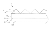
- FIGS. 3 and 4 the preferred embodiment of a prismatic laminate 3 according to this invention is shown to be disposed on a planar light source unit 2 for a liquid crystal display and the like.
- the planar light source unit 2 includes alight guide plate 21 , a light source 22 , and a reflecting sheet 23 .
- the light guide plate 21 has a light-incident surface 211 , a bottom surface 212 , and a light-exiting surface 213 opposite to the bottom surface 212 .
- the light source 22 is bonded to the light-incident surface 211 .
- the reflecting sheet 23 is bonded to the bottom surface 212 .
- the prismatic laminate 3 is disposed on the light-exiting surface 213 , and includes a prismatic structure 31 and an optical layer 32 .
- the prismatic structure 31 includes a plate body 311 having a first surface 313 distal from the planar light source unit 2 and a second surface 314 opposite to the first surface 313 , and a plurality of prismatic strips 312 formed on the first surface 313 of the plate body 311 .
- the plate body 311 and the prismatic strips 312 are independently made of transparent materials.
- the plate body 311 is made of polyester, such as polyethylene terephthalate, and the prismatic strips 312 are made of ultra-violet curable resin.
- Each of the prismatic strips 312 has a triangular cross-section.
- the optical layer 32 is formed on the second surface 314 of the plate body 311 , and has a thickness ranging from 2 to 30 ⁇ m.
- the optical layer 32 includes a base part 321 bonded to the second surface 314 of the plate body 311 , and a plurality of microstructures 322 protruding from the base part 321 in a direction away from the second surface 314 of the plate body 311 .
- Each of the microstructures 322 has a protruding height ranging from 0.05 ⁇ m to 0.5 ⁇ m.
- the light emitted from the light source 22 enters into the light guide plate 21 via the light-incident surface 211 , is guided by the light guide plate 21 and the reflecting sheet 23 so as to exit the light guide plate 21 via the light-exiting surface 213 , and travels to the prismatic laminate 3 .
- the light reaching the optical layer 32 of the prismatic laminate 3 is diffused via the microstructures 322 , travels to the prismatic structure 31 , and is refracted by the prismatic strips 312 so as to achieve a purpose of improving a luminance of a display (not shown).
- each of the microstructures 322 preferably has a protruding height ranging from 0.05 ⁇ m to 0.5 ⁇ m so as to control the haze of the microstructures 322 to be in a range from 5 to 20% while retaining a high transmittance of not less than 85%. If the protruding height is less than 0.05 ⁇ m, the haze is unsatisfactory. On the other hand, if the protruding height is more than 0.5 ⁇ m, the transmittance is insufficient.
- the optical layer 32 is formed from a coating including a transparent resin component and an antistatic agent.
- the transparent resin component is a thermoplastic resin or an ultra-violet curable resin.
- the thermoplastic resin suitable for the present invention include, but are not limited to, polyester, polyamide, polypropylene, polyvinyl chloride, polyethylene methyl methylacrylate, polycarbonate, or combinations thereof.
- the ultra-violet curable resin can be cross-linked and cured by irradiation of ultra-violet light.
- the ultra-violet curable resin includes an ultra-violet curable monomer and an ultra-violet curable oligomer, and a photo-initiator.
- ultra-violet curable monomer suitable for the present invention examples include, but are not limited to, styrenic monomers; acrylates, such as methyl acrylate, methoxy ethyl acrylate, tripropylene glycol diacrylate, dipropylene glycol diacrylate, 2-phenoxy ethyl acrylate, 1,6-hexylene glycol diacrylate, and butyl acrylate; and methacrylates, such as methyl methacrylate, ethyl methacrylate, and methoxy ethyl methacrylate; and combinations thereof.
- styrenic monomers examples include, but are not limited to, styrenic monomers; acrylates, such as methyl acrylate, methoxy ethyl acrylate, tripropylene glycol diacrylate, dipropylene glycol diacrylate, 2-phenoxy ethyl acrylate, 1,6-hexylene glycol diacrylate, and butyl
- photo-initiator suitable for the present invention examples include, but are riot limited to, acetophenone, benzophenone, acylphosphine oxide, and combinations thereof.
- any suitable additives commonly used in the art can be added if desired.
- a sensitizer can be added to increase photo-sensitivity of the ultra-violet curable resin.
- Oligomers such as polyester acrylate oligomers, epoxy acrylate oligomers, urethane acrylate oligomers, full acrylate oligomers, or the like can be added to adjust mechanical properties of the ultra-violet curable resin for specific requirements.
- the transparent resin component for the optical layer 32 is similar to the material for the prismatic structure 31 so as to avoid warping or waving of the optical layer 32 and the prismatic structure 31 due to the difference in the thermal expansion coefficients therebetween.
- the transparent resin component includes an ultra-violet curable acrylate resin and benzophenone.
- the antistatic agent is used for reducing surface resistance of the optical layer 32 so as to decrease an optical coupling phenomenon and a scratching problem due to static absorption of particles during assembly the prismatic structure 31 to the optical layer 32 . It is found that the static absorption can be effectively decreased when the surface resistance of the optical layer 32 is not more than 10 13 ⁇ / ⁇ .
- the optical layer 32 has a surface resistance ranging from 10 10 to 10 13 ⁇ / ⁇ , which can be obtained when the antistatic agent is used in an amount ranging from 5 to 25 wt % of the coating for forming the optical layer 32 .
- the antistatic agent suitable for the present invention include, but are not limited to, metallic conductive particle, metal oxide, a quarternary ammonium salt, or combinations thereof.
- the antistatic agent used in the preferred embodiment is quarternary ammonium salt.
- a back-coating roller which has a roller surface with a plurality of recesses arranged in a predetermined pattern.
- the recesses are produced by laser holography. Specifically, a pattern to be formed on a mask is determined using Fourier analysis. The mask having the pattern is produced using laser holography.
- the back-coating roller is formed by lithography via the mask so as to form a plurality of recesses, which are arranged in a pattern corresponding to that formed on the mask, on the roller surface of the back-coating roller.
- a protective layer is applied on the back-coating roller by plating on the roller surface to protect the surfaces of the recesses so as to increase abrasion resistance of the surfaces of the recesses.
- the uniformity of the recesses can be improved by virtue of the protective layer so as to precisely control the uniformity of the microstructures 322 to be formed on the optical layer 32 .
- a prismatic structure which includes a plate body having a first surface and a second surface opposite to the first surface, and a plurality of prismatic strips formed on the first surface of the plate body.
- a coating containing a resin component and an antistatic agent is applied on the second surface of the plate body in a roll-to-roll manner.
- the resin component used in the preferred embodiment is an ultra-violet curable resin including an ultra-violet curable monomer and an ultra-violet curable oligomer, and a photo-initiator.
- the coating is embossed with the back-coating roller while being cured by an ultra-violet irradiation to form an optical layer including a plurality of microstructures protruding in a direction away from the second surface of the plate body and having a pattern corresponding to that of the recesses in the roller surface.
- the back-coating roller having uniform and precise recesses can be formed via laser holography and lithography, the microstructures 322 of the optical layer 32 formed thereby can be controlled precisely to have a uniform protruding height ranging from 0.05 ⁇ m to 0.5 ⁇ m. Therefore, satisfactory haze and transmittance can be obtained for the optical layer 32 .
Landscapes
- Physics & Mathematics (AREA)
- General Physics & Mathematics (AREA)
- Optics & Photonics (AREA)
- Optical Elements Other Than Lenses (AREA)
- Laminated Bodies (AREA)
- Planar Illumination Modules (AREA)
Abstract
Description
Claims (10)
Applications Claiming Priority (3)
| Application Number | Priority Date | Filing Date | Title |
|---|---|---|---|
| TW98127260A | 2009-08-13 | ||
| TW098127260 | 2009-08-13 | ||
| TW098127260A TWI404978B (en) | 2009-08-13 | 2009-08-13 | Prism with optical layer and its making method |
Publications (2)
| Publication Number | Publication Date |
|---|---|
| US20110038052A1 US20110038052A1 (en) | 2011-02-17 |
| US8089697B2 true US8089697B2 (en) | 2012-01-03 |
Family
ID=43588448
Family Applications (1)
| Application Number | Title | Priority Date | Filing Date |
|---|---|---|---|
| US12/652,216 Expired - Fee Related US8089697B2 (en) | 2009-08-13 | 2010-01-05 | Prismatic laminate and method for making the same |
Country Status (2)
| Country | Link |
|---|---|
| US (1) | US8089697B2 (en) |
| TW (1) | TWI404978B (en) |
Families Citing this family (2)
| Publication number | Priority date | Publication date | Assignee | Title |
|---|---|---|---|---|
| EP2431786A1 (en) * | 2010-09-17 | 2012-03-21 | Bayer MaterialScience AG | Autostereoscopic 3D display |
| TWI668476B (en) * | 2018-11-23 | 2019-08-11 | 茂林光電科技股份有限公司 | Light guide plate, light guide module and processing apparatus of light microstructure |
Citations (3)
| Publication number | Priority date | Publication date | Assignee | Title |
|---|---|---|---|---|
| US6280063B1 (en) * | 1997-05-09 | 2001-08-28 | 3M Innovative Properties Company | Brightness enhancement article |
| US20090122577A1 (en) * | 2007-11-09 | 2009-05-14 | Eternal Chemical Co., Ltd. | Optical Film |
| US20110068305A1 (en) * | 2009-09-18 | 2011-03-24 | Eternal Chemical Co., Ltd. | Polymerizable composition and its uses |
Family Cites Families (2)
| Publication number | Priority date | Publication date | Assignee | Title |
|---|---|---|---|---|
| TW200846715A (en) * | 2006-12-18 | 2008-12-01 | Kolon Inc | Optical sheets |
| TW200918954A (en) * | 2007-10-23 | 2009-05-01 | Optivision Technology Inc | Diffusive brightness enhancement film |
-
2009
- 2009-08-13 TW TW098127260A patent/TWI404978B/en not_active IP Right Cessation
-
2010
- 2010-01-05 US US12/652,216 patent/US8089697B2/en not_active Expired - Fee Related
Patent Citations (3)
| Publication number | Priority date | Publication date | Assignee | Title |
|---|---|---|---|---|
| US6280063B1 (en) * | 1997-05-09 | 2001-08-28 | 3M Innovative Properties Company | Brightness enhancement article |
| US20090122577A1 (en) * | 2007-11-09 | 2009-05-14 | Eternal Chemical Co., Ltd. | Optical Film |
| US20110068305A1 (en) * | 2009-09-18 | 2011-03-24 | Eternal Chemical Co., Ltd. | Polymerizable composition and its uses |
Also Published As
| Publication number | Publication date |
|---|---|
| TW201106023A (en) | 2011-02-16 |
| US20110038052A1 (en) | 2011-02-17 |
| TWI404978B (en) | 2013-08-11 |
Similar Documents
| Publication | Publication Date | Title |
|---|---|---|
| US7626761B2 (en) | Fly's-eye lens sheet having light-shielding layer, method for fabricating the same, transmissive screen, and rear projection image display device | |
| CN101004461B (en) | Anti-scratch film and liquid crystal display | |
| JP4468972B2 (en) | Microstructure-containing products | |
| US7472999B2 (en) | Antiglare film, process for producing the same, and display device using antiglare film | |
| KR101204597B1 (en) | Scratch-resistant thin film | |
| CN100485429C (en) | Thin type flexible light-guiding component | |
| KR20100037146A (en) | Prism sheet, and backlight unit and liquid crystal display device using prism sheet | |
| KR20120101401A (en) | Optical film with anti-warp surface | |
| KR20080109658A (en) | Scratching resistant optical film comprising organic particles with very uniform particle size | |
| KR101097518B1 (en) | Newton ring prevention sheet, and touch panel using this | |
| KR20150095198A (en) | Anti-glare film | |
| KR20190017662A (en) | A buffer sheet and a flat panel display | |
| JP5521357B2 (en) | Prism sheet, backlight unit using the same, and liquid crystal display device | |
| TWI635358B (en) | Hard coating film and display element with surface member | |
| KR20160015160A (en) | Anti-glare film | |
| JP2003205564A (en) | Antistatic transfer foil with antireflection function | |
| JP2005031282A (en) | Resin composition for optical element, cured resin for optical element, and optical element | |
| KR20160015161A (en) | Anti-glare film | |
| US8089697B2 (en) | Prismatic laminate and method for making the same | |
| JP5603541B2 (en) | Prism sheet | |
| CN100430755C (en) | Lenticular sheets, transmissive screens, and rear projection displays | |
| KR100785889B1 (en) | Diffusion protection film, a back light unit including the diffusion protection film and a manufacturing method thereof | |
| KR20110082327A (en) | Reflective Sheet for Backlight Unit | |
| JP5603542B2 (en) | Prism sheet | |
| TW201938359A (en) | Antiglare film |
Legal Events
| Date | Code | Title | Description |
|---|---|---|---|
| AS | Assignment |
Owner name: OPTIVISION TECHNOLOGY INC., TAIWAN Free format text: ASSIGNMENT OF ASSIGNORS INTEREST;ASSIGNORS:LOR, WHEY-BIN;YUAN, KUANG-LIN;HUANG, RU-PING;AND OTHERS;REEL/FRAME:023735/0339 Effective date: 20091207 |
|
| ZAAA | Notice of allowance and fees due |
Free format text: ORIGINAL CODE: NOA |
|
| ZAAB | Notice of allowance mailed |
Free format text: ORIGINAL CODE: MN/=. |
|
| STCF | Information on status: patent grant |
Free format text: PATENTED CASE |
|
| FEPP | Fee payment procedure |
Free format text: PAT HOLDER CLAIMS SMALL ENTITY STATUS, ENTITY STATUS SET TO SMALL (ORIGINAL EVENT CODE: LTOS); ENTITY STATUS OF PATENT OWNER: SMALL ENTITY |
|
| FPAY | Fee payment |
Year of fee payment: 4 |
|
| MAFP | Maintenance fee payment |
Free format text: PAYMENT OF MAINTENANCE FEE, 8TH YR, SMALL ENTITY (ORIGINAL EVENT CODE: M2552); ENTITY STATUS OF PATENT OWNER: SMALL ENTITY Year of fee payment: 8 |
|
| FEPP | Fee payment procedure |
Free format text: MAINTENANCE FEE REMINDER MAILED (ORIGINAL EVENT CODE: REM.); ENTITY STATUS OF PATENT OWNER: SMALL ENTITY |
|
| LAPS | Lapse for failure to pay maintenance fees |
Free format text: PATENT EXPIRED FOR FAILURE TO PAY MAINTENANCE FEES (ORIGINAL EVENT CODE: EXP.); ENTITY STATUS OF PATENT OWNER: SMALL ENTITY |
|
| STCH | Information on status: patent discontinuation |
Free format text: PATENT EXPIRED DUE TO NONPAYMENT OF MAINTENANCE FEES UNDER 37 CFR 1.362 |
|
| FP | Lapsed due to failure to pay maintenance fee |
Effective date: 20240103 |