US8089612B2 - Position detection apparatus, position detection method, exposure apparatus, and device fabrication method - Google Patents
Position detection apparatus, position detection method, exposure apparatus, and device fabrication method Download PDFInfo
- Publication number
- US8089612B2 US8089612B2 US12/412,295 US41229509A US8089612B2 US 8089612 B2 US8089612 B2 US 8089612B2 US 41229509 A US41229509 A US 41229509A US 8089612 B2 US8089612 B2 US 8089612B2
- Authority
- US
- United States
- Prior art keywords
- light
- target object
- light beams
- optical system
- imaging
- Prior art date
- Legal status (The legal status is an assumption and is not a legal conclusion. Google has not performed a legal analysis and makes no representation as to the accuracy of the status listed.)
- Expired - Fee Related, expires
Links
- 238000001514 detection method Methods 0.000 title claims abstract description 100
- 238000000034 method Methods 0.000 title claims description 32
- 238000004519 manufacturing process Methods 0.000 title claims description 3
- 230000003287 optical effect Effects 0.000 claims abstract description 233
- 238000003384 imaging method Methods 0.000 claims abstract description 115
- 230000006866 deterioration Effects 0.000 claims abstract description 17
- 230000002194 synthesizing effect Effects 0.000 claims abstract description 6
- 238000005315 distribution function Methods 0.000 claims description 48
- 230000006870 function Effects 0.000 claims description 22
- 239000000758 substrate Substances 0.000 claims description 17
- 238000012546 transfer Methods 0.000 claims description 16
- 230000008569 process Effects 0.000 claims description 13
- 238000000926 separation method Methods 0.000 claims description 6
- 238000011161 development Methods 0.000 claims description 2
- 238000003860 storage Methods 0.000 description 17
- 238000005286 illumination Methods 0.000 description 13
- 238000004364 calculation method Methods 0.000 description 12
- 238000009826 distribution Methods 0.000 description 11
- 230000004075 alteration Effects 0.000 description 6
- 239000010408 film Substances 0.000 description 6
- 239000004065 semiconductor Substances 0.000 description 6
- 230000009466 transformation Effects 0.000 description 4
- 230000009471 action Effects 0.000 description 3
- 230000005540 biological transmission Effects 0.000 description 3
- 238000013461 design Methods 0.000 description 3
- 238000005259 measurement Methods 0.000 description 3
- 230000003595 spectral effect Effects 0.000 description 3
- 238000012935 Averaging Methods 0.000 description 2
- 238000012937 correction Methods 0.000 description 2
- 238000010586 diagram Methods 0.000 description 2
- 238000005530 etching Methods 0.000 description 2
- 239000011521 glass Substances 0.000 description 2
- 229910052736 halogen Inorganic materials 0.000 description 2
- 150000002367 halogens Chemical class 0.000 description 2
- 239000004973 liquid crystal related substance Substances 0.000 description 2
- 230000035945 sensitivity Effects 0.000 description 2
- 239000010409 thin film Substances 0.000 description 2
- 239000013598 vector Substances 0.000 description 2
- 230000008901 benefit Effects 0.000 description 1
- 230000015572 biosynthetic process Effects 0.000 description 1
- 239000003795 chemical substances by application Substances 0.000 description 1
- 239000002131 composite material Substances 0.000 description 1
- 230000008602 contraction Effects 0.000 description 1
- 210000002858 crystal cell Anatomy 0.000 description 1
- 230000003247 decreasing effect Effects 0.000 description 1
- 239000005262 ferroelectric liquid crystals (FLCs) Substances 0.000 description 1
- 238000010438 heat treatment Methods 0.000 description 1
- 239000011229 interlayer Substances 0.000 description 1
- 235000019557 luminance Nutrition 0.000 description 1
- 238000012986 modification Methods 0.000 description 1
- 230000004048 modification Effects 0.000 description 1
- 230000002093 peripheral effect Effects 0.000 description 1
- 238000000206 photolithography Methods 0.000 description 1
- 238000003672 processing method Methods 0.000 description 1
- 230000003252 repetitive effect Effects 0.000 description 1
- 238000004904 shortening Methods 0.000 description 1
- 238000002834 transmittance Methods 0.000 description 1
- 230000004304 visual acuity Effects 0.000 description 1
Images


Classifications
-
- G—PHYSICS
- G01—MEASURING; TESTING
- G01B—MEASURING LENGTH, THICKNESS OR SIMILAR LINEAR DIMENSIONS; MEASURING ANGLES; MEASURING AREAS; MEASURING IRREGULARITIES OF SURFACES OR CONTOURS
- G01B11/00—Measuring arrangements characterised by the use of optical techniques
- G01B11/02—Measuring arrangements characterised by the use of optical techniques for measuring length, width or thickness
- G01B11/024—Measuring arrangements characterised by the use of optical techniques for measuring length, width or thickness by means of diode-array scanning
-
- G—PHYSICS
- G03—PHOTOGRAPHY; CINEMATOGRAPHY; ANALOGOUS TECHNIQUES USING WAVES OTHER THAN OPTICAL WAVES; ELECTROGRAPHY; HOLOGRAPHY
- G03B—APPARATUS OR ARRANGEMENTS FOR TAKING PHOTOGRAPHS OR FOR PROJECTING OR VIEWING THEM; APPARATUS OR ARRANGEMENTS EMPLOYING ANALOGOUS TECHNIQUES USING WAVES OTHER THAN OPTICAL WAVES; ACCESSORIES THEREFOR
- G03B27/00—Photographic printing apparatus
- G03B27/32—Projection printing apparatus, e.g. enlarger, copying camera
-
- G—PHYSICS
- G03—PHOTOGRAPHY; CINEMATOGRAPHY; ANALOGOUS TECHNIQUES USING WAVES OTHER THAN OPTICAL WAVES; ELECTROGRAPHY; HOLOGRAPHY
- G03F—PHOTOMECHANICAL PRODUCTION OF TEXTURED OR PATTERNED SURFACES, e.g. FOR PRINTING, FOR PROCESSING OF SEMICONDUCTOR DEVICES; MATERIALS THEREFOR; ORIGINALS THEREFOR; APPARATUS SPECIALLY ADAPTED THEREFOR
- G03F9/00—Registration or positioning of originals, masks, frames, photographic sheets or textured or patterned surfaces, e.g. automatically
- G03F9/70—Registration or positioning of originals, masks, frames, photographic sheets or textured or patterned surfaces, e.g. automatically for microlithography
- G03F9/7003—Alignment type or strategy, e.g. leveling, global alignment
- G03F9/7046—Strategy, e.g. mark, sensor or wavelength selection
-
- G—PHYSICS
- G03—PHOTOGRAPHY; CINEMATOGRAPHY; ANALOGOUS TECHNIQUES USING WAVES OTHER THAN OPTICAL WAVES; ELECTROGRAPHY; HOLOGRAPHY
- G03F—PHOTOMECHANICAL PRODUCTION OF TEXTURED OR PATTERNED SURFACES, e.g. FOR PRINTING, FOR PROCESSING OF SEMICONDUCTOR DEVICES; MATERIALS THEREFOR; ORIGINALS THEREFOR; APPARATUS SPECIALLY ADAPTED THEREFOR
- G03F9/00—Registration or positioning of originals, masks, frames, photographic sheets or textured or patterned surfaces, e.g. automatically
- G03F9/70—Registration or positioning of originals, masks, frames, photographic sheets or textured or patterned surfaces, e.g. automatically for microlithography
- G03F9/7065—Production of alignment light, e.g. light source, control of coherence, polarization, pulse length, wavelength
-
- G—PHYSICS
- G03—PHOTOGRAPHY; CINEMATOGRAPHY; ANALOGOUS TECHNIQUES USING WAVES OTHER THAN OPTICAL WAVES; ELECTROGRAPHY; HOLOGRAPHY
- G03F—PHOTOMECHANICAL PRODUCTION OF TEXTURED OR PATTERNED SURFACES, e.g. FOR PRINTING, FOR PROCESSING OF SEMICONDUCTOR DEVICES; MATERIALS THEREFOR; ORIGINALS THEREFOR; APPARATUS SPECIALLY ADAPTED THEREFOR
- G03F9/00—Registration or positioning of originals, masks, frames, photographic sheets or textured or patterned surfaces, e.g. automatically
- G03F9/70—Registration or positioning of originals, masks, frames, photographic sheets or textured or patterned surfaces, e.g. automatically for microlithography
- G03F9/7088—Alignment mark detection, e.g. TTR, TTL, off-axis detection, array detector, video detection
Definitions
- the present invention relates to a position detection apparatus, a position detection method, an exposure apparatus, and a device fabrication method.
- a projection exposure apparatus has conventionally been employed to fabricate a micropatterned semiconductor device such as a semiconductor memory or logic circuit by using photolithography.
- the projection exposure apparatus projects and transfers a circuit pattern formed on a reticle (mask) onto a substrate such as a wafer by a projection optical system.
- the projection exposure apparatus is being required to improve the resolving power (a minimum feature size that it can transfer).
- the wavelength of the exposure light is shortening, high-NA projection optical systems are under development (the numerical aperture (NA) of the projection optical system is increasing), and the exposure region is widening.
- the projection exposure apparatus is also being required to align the reticle and the wafer with an accuracy as high as 1 ⁇ 3 the line width of the circuit pattern.
- a typical current circuit designed to have a line width of 90 nm must be aligned with an accuracy of 30 nm.
- the exposure apparatus performs the alignment by transferring an alignment mark onto a wafer, together with the circuit pattern, and detects the position of the alignment mark in transferring the next circuit pattern onto the wafer, thereby aligning the wafer with the reticle.
- the alignment mark transferred onto the wafer is optically detected by, for example, a position detection apparatus (image sensing apparatus) 1000 as shown in FIG. 21 .
- FIG. 21 is a schematic view showing a conventional position detection apparatus 1000 .
- a light source 1002 is deflected by a beam splitter 1004 , and illuminates an alignment mark (target object) 1010 , which is transferred onto a wafer 1008 , via an imaging optical system 1006 .
- the light reflected by the alignment mark 1010 forms an image on an image sensor 1012 via the imaging optical system 1006 , and is sensed by the image sensor 1012 as the optical image (light intensity distribution) of the alignment mark 1010 .
- a known technique corrects deterioration in the optical image (light intensity distribution) of the alignment mark 1010 attributed to the optical system of the position detection apparatus 1000 , and restores an optical image of the alignment mark 1010 by measuring the optical transfer function of the imaging optical system 1006 in advance and using an inverse filter.
- G ( ⁇ ) H ( ⁇ ) ⁇ F ( ⁇ ) (1)
- G( ⁇ ) is the Fourier transform of g(x)
- F( ⁇ ) is the Fourier transform of f(x)
- H( ⁇ ) is the Fourier transform of a point image distribution function (PSF: Point Spread Function) or a line image distribution function (LSF: Line Spread Function) and represents the imaging characteristic of the imaging optical system 1006 .
- PSF Point Spread Function
- LSF Line Spread Function
- Japanese Patent Laid-Open No. 2004-281904 proposes a technique of measuring, for example, the optical transfer function and electrical transfer function of the position detection apparatus in advance, thereby correcting deterioration in the optical image (light intensity distribution) using these two transfer functions.
- the prior art measures, using broadband light as the illumination light, the PSF or LSF over the entire wavelength width of the illumination light.
- deterioration in the optical image is corrected using an optical transfer function G( ⁇ ) as the Fourier transform of the PSF or LSF.
- the optical transfer function G( ⁇ ) which includes the information of the influence of aberrations in the optical system has a wavelength dependence. This is because aberrations (for example, an on-axis chromatic aberration) in the optical system generally differ in their generation amounts (aberration amounts) among wavelengths. For this reason, if differences in light intensity occur among wavelengths between when the PSF or LSF is measured and when a target object such as an alignment mark is measured, it is impossible to satisfactorily correct deterioration in the optical image (light intensity distribution).
- FIG. 22 is a graph showing the wavelength dependence of the reflectance of the wafer (alignment mark) serving as the target object.
- the ordinate indicates the reflectance of the wafer
- the abscissa indicates the wavelength of light which illuminates the wafer.
- 2004-281904 does not take account of the wavelength dependence of the reflectance of the wafer (alignment mark). Therefore, even when the PSF or LSF is calculated over the entire wavelength width of the illumination light, and an optical transfer function G( ⁇ ) as its Fourier transform is used, the optical image (light intensity distribution) changes depending on the wavelength. This makes it impossible to satisfactorily correct deterioration in the optical image.
- the present invention provides a position detection apparatus which can accurately detect the position of a target object.
- a position detection apparatus which detects a position of a target object
- the apparatus comprising a light source configured to emit light having a wavelength width onto the target object, an imaging optical system configured to form an image of the light from the target object on an image sensor, a first obtaining unit configured to obtain imaging characteristics of the imaging optical system for a plurality of light beams, having different wavelength with each other, of the light having the wavelength width, a second obtaining unit configured to obtain optical images of the target object for the plurality of the light beams, a restoration unit configured to restore optical images of the target object for the plurality of the light beams by correcting, deterioration in the optical images of the target object obtained by the second obtaining unit attributed to the imaging optical system, based on the imaging characteristics of the imaging optical system obtained by the first obtaining unit, a generation unit configured to generate an optical image of the target object for light including the plurality of the light beams by synthesizing the optical images of the target object for the plurality of the light
- FIG. 1 is a schematic view showing a position detection apparatus according to one aspect of the present invention.
- FIG. 2 is a schematic view showing the detailed configuration of a wavelength selection unit in the position detection apparatus shown in FIG. 1 .
- FIG. 3 is a graph showing the spectral characteristics of a plurality of bandpass filters of the wavelength selection unit shown in FIG. 2 .
- FIGS. 4A and 4B are flowcharts for explaining a position detection method according to one aspect of the present invention.
- FIG. 5 is a graph showing an example of the line image distribution functions of an imaging optical system obtained in an imaging characteristic obtaining step.
- FIG. 6 is a graph showing an example of the optical images of a target pattern obtained in an optical image obtaining step.
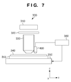
- FIG. 7 is a schematic view showing an exposure apparatus according to one aspect of the present invention.
- FIG. 8 is a schematic view showing an arrangement of an alignment detection system in the exposure apparatus shown in FIG. 1 .
- FIGS. 9A and 9B are views showing an example of an alignment mark on a wafer.
- FIG. 10 is a chart showing the image (detection result) of the alignment mark sensed by a line sensor when the alignment mark shown in FIGS. 9A and 9B is used.
- FIGS. 11A to 11C are charts for explaining a template matching method.
- FIG. 12 is a view showing a misalignment of the shot array on the wafer with respect to the x-y coordinate system on a wafer stage of the exposure apparatus shown in FIG. 1 .
- FIG. 13 is a diagram schematically showing, using vectors, a linear coordinate transform shown in equation (15).
- FIG. 14 is a schematic view showing another arrangement of the alignment detection system in the exposure apparatus shown in FIG. 1 .
- FIG. 15 is a graph showing the reflectance characteristics of dichroic mirrors of the alignment detection system shown in FIG. 14 .
- FIG. 16 is a schematic view showing still another arrangement of the alignment detection system in the exposure apparatus shown in FIG. 1 .
- FIG. 17 is a schematic view showing the structure of a bandpass filter of the alignment detection system shown in FIG. 16 .
- FIG. 18 is a view showing an optical image of an alignment mark formed on an area sensor of the alignment detection system shown in FIG. 16 .
- FIG. 19 is a schematic view showing still another arrangement of the alignment detection system in the exposure apparatus shown in FIG. 1 .
- FIG. 20 is a view showing the diffraction (splitting) action of a diffraction grating of the alignment detection system shown in FIG. 19 .
- FIG. 21 is a schematic view showing a conventional position detection apparatus.
- FIG. 22 is a graph showing an example of the wavelength dependence of the reflectance of a wafer (alignment mark) serving as the target object.
- FIG. 1 is a schematic view showing a position detection apparatus 1 according to one aspect of the present invention.
- the position detection apparatus 1 detects the position of a target object T (target pattern TP).
- the position detection apparatus 1 includes a light source 11 , wavelength selection unit 12 , beam splitter 13 , imaging optical system 14 , image sensor 15 , first storage unit 16 , second storage unit 17 , calculation unit 18 , output unit 19 , stage 20 , and imaging characteristic obtaining pattern 21 .
- the light source 11 is, for example, a halogen lamp and emits light having a wavelength width (i.e., broadband light).
- the wavelength selection unit 12 selectively passes light beams having predetermined wavelengths (light beams having a plurality of different wavelengths) of the light which has a wavelength width and is emitted by the light source 11 .
- the wavelength selection unit 12 includes a plurality of bandpass filters 122 a to 122 j which pass light beams having a plurality of wavelengths, and a turret 124 which exchangeably inserts the bandpass filters 122 a to 122 j into the optical path between the light source 11 and the target object T, as shown in FIG. 2 .
- the bandpass filters 122 a to 122 j exhibit, for example, characteristics having a transmission wavelength width of about 30 nm and transmission center wavelengths shifted from each other by 20 nm, as shown in FIG.
- the target object T can be illuminated with light having an arbitrary wavelength by inserting an arbitrary one of the bandpass filters 122 a to 122 j into the optical path by rotating the turret 124 in the wavelength selection unit 12 .
- FIG. 2 is a schematic view showing the detailed configuration of the wavelength selection unit 12 .
- FIG. 3 is a graph showing the spectral characteristics of the plurality of bandpass filters 122 a to 122 j of the wavelength selection unit 12 .
- the wavelength selection unit 12 is not particularly limited to the configuration shown in FIG. 2 .
- a bandpass filter manufactured by a combination of a birefringent plate and a ferroelectric liquid crystal cell may be used.
- the function of the wavelength selection unit 12 may be imparted to the light source 11 by, for example, using a Ti-sapphire laser having a variable wavelength or an optical frequency comb generator for the light source 11 , or constituting the light source 11 by a plurality of light sources which emit light beams having different wavelengths.
- the beam splitter 13 reflects the light having passed through the wavelength selection unit 12 to the target object T (target pattern TP) or the imaging characteristic obtaining pattern 21 . Also, the beam splitter 13 transmits the light from the target object T (target pattern TP) or the imaging characteristic obtaining pattern 21 to the image sensor 15 .
- the imaging optical system 14 guides the light from the target pattern TP on the target object T or the imaging characteristic obtaining pattern 21 onto the image sensor 15 to form an optical image (light intensity distribution) of the target pattern TP or the imaging characteristic obtaining pattern 21 on the image sensor 15 .
- the image sensor 15 senses the optical image of the target pattern TP or the imaging characteristic obtaining pattern 21 formed by the imaging optical system 14 .
- the first storage unit 16 stores point image distribution functions PSF( ⁇ ) or line image distribution functions LSF( ⁇ ) of the imaging optical system 14 as the imaging characteristics of the imaging optical system 14 for the plurality of different wavelengths ⁇ selected by the wavelength selection unit 12 .
- the second storage unit 17 stores optical images g( ⁇ ) of the target pattern TP for the plurality of different wavelengths ⁇ selected by the wavelength selection unit 12 . Note that the optical images g( ⁇ ) of the target pattern TP stored in the second storage unit 17 include deterioration attributed to the imaging optical system 14 .
- the calculation unit 18 corrects the deterioration in the optical images g( ⁇ ) attributed to the imaging optical system 14 based on the point image distribution functions PSF( ⁇ ) or the line image distribution functions LSF( ⁇ ), thereby restoring optical images f( ⁇ ) of the target pattern TP for the plurality of wavelengths ⁇ . Also, the calculation unit 18 composites the restored optical images f( ⁇ ) to generate an optical image of the target pattern TP for light including the plurality of wavelengths ⁇ , and determines the position of the target object T (target pattern TP) based on the optical image of the target pattern TP.
- the calculation unit 18 serves as a restoration unit which restores an optical image of the target pattern TP, a generation unit which generates an optical image of the target pattern TP for light having an arbitrary wavelength, and a determination unit which determines the position of the target pattern TP (target object T).
- the output unit 19 outputs or displays the optical image of the target pattern TP generated (calculated) by the calculation unit 18 .
- the stage 20 holds the target object T and the imaging characteristic obtaining pattern 21 , and drives the target object T (target pattern TP) or the imaging characteristic obtaining pattern 21 beneath the imaging optical system 14 .
- the imaging characteristic obtaining pattern 21 is a pattern to obtain the imaging characteristics of the imaging optical system 14 (the point image distribution functions PSF( ⁇ ) or line image distribution functions LSF( ⁇ ) of the imaging optical system 14 ), and includes, for example, a slit pattern or a pinhole pattern.
- a pinhole pattern is used as the imaging characteristic obtaining pattern 21 in order to obtain the point image distribution functions PSF( ⁇ ) as the imaging characteristics of the imaging optical system 14 .
- the target pattern TP is a one-dimensional pattern (a pattern which changes along the x-axis and is constant along the y-axis)
- a slit pattern whose slit width direction is the x-axis direction is used as the imaging characteristic obtaining pattern 21 in order to obtain the line image distribution functions LSF( ⁇ ) as the imaging characteristics of the imaging optical system 14 .
- the point image distribution functions PSF( ⁇ ) or the line image distribution functions LSF( ⁇ ) of the imaging optical system 14 can be obtained (measured) by a method known to those skilled in the art.
- To obtain the line image distribution function LSF( ⁇ ) it is only necessary to form, on the image sensor 15 via the imaging optical system 14 , an image of light reflected by or transmitted through a slit pattern serving as the imaging characteristic obtaining pattern 21 , and to sense the optical image (light intensity distribution).
- a diameter d of the pinhole pattern or a slit width d of the slit pattern used as the imaging characteristic obtaining pattern 21 , and the numerical aperture NA of the imaging optical system 14 satisfy: d ⁇ 1 ⁇ 2 ⁇ /NA (3)
- this embodiment will exemplify a case in which the target pattern TP is a one-dimensional pattern, and the line image distribution functions LSF( ⁇ ) are used as the imaging characteristics of the imaging optical system 14 . If the target pattern TP is a two-dimensional pattern, the following description need only be applied to the point image distribution functions PSF( ⁇ ) assuming the y-axis as well as the x-axis.
- FIGS. 4A and 4B are flowcharts for explaining a position detection method according to one aspect of the present invention.
- the position detection method in the position detection apparatus 1 is roughly divided into three steps: an imaging characteristic obtaining step (S 600 ), an optical image obtaining step (S 700 ), and an optical image restoration step (S 800 ), as shown in FIG. 4A .
- the imaging characteristic obtaining step (S 600 ) as a first obtaining step, the imaging characteristics (in this embodiment, the line image distribution functions LSF( ⁇ )) of the imaging optical system 14 are obtained (measured).
- the optical image obtaining step (S 700 ) as a second obtaining step, the optical images of the target pattern TP on the target object T are obtained (measured).
- the optical image restoration step (S 800 ) optical images of the target pattern TP are restored by correcting deterioration in the optical images of the target pattern TP attributed to the imaging optical system 14 .
- a reflective slit pattern serving as the imaging characteristic obtaining pattern 21 is arranged beneath the imaging optical system 14 through the stage 20 in order to obtain (measure) the line image distribution functions LSF( ⁇ ) of the imaging optical system 14 .
- the light source 11 , wavelength selection unit 12 , beam splitter 13 , imaging optical system 14 , image sensor 15 , and imaging characteristic obtaining pattern 21 serve as a first obtaining unit for obtaining the imaging characteristics of the imaging optical system 14 .
- step S 602 a wavelength ⁇ 1 of light (illumination light) which illuminates the slit pattern serving as the imaging characteristic obtaining pattern 21 is selected by the wavelength selection unit 12 .
- step S 604 the slit pattern is illuminated with a light beam having the wavelength ⁇ 1 selected in step S 602 , and the optical image of the slit pattern is sensed by the image sensor 15 , thereby obtaining a line image distribution function LSF( ⁇ 1 ).
- step S 606 the line image distribution function LSF( ⁇ 1 ) obtained in step S 604 is stored in the first storage unit 16 .
- step S 608 it is checked whether the line image distribution functions LSF for all light beams having different wavelengths which can be selected by the wavelength selection unit 12 (in this embodiment, light beams which pass through the bandpass filters 122 a to 122 j ) have been obtained. If it is determined that the line image distribution functions LSF for all light beams having different wavelengths which can be selected by the wavelength selection unit 12 have been obtained, the process advances to the optical image obtaining step (S 700 ).
- step S 602 if it is determined that the line image distribution functions LSF for all light beams having different wavelengths which can be selected by the wavelength selection unit 12 have not yet been obtained, the process returns to step S 602 , and the next wavelength ⁇ 2 is selected by the wavelength selection unit 12 , and steps S 604 and S 606 are executed.
- FIG. 5 shows an example of line image distribution functions LSF(x, ⁇ ) of the imaging optical system 14 obtained in the imaging characteristic obtaining step (S 600 ) in this way.
- FIG. 5 shows only line image distribution functions LSF(x, ⁇ ) for light beams having the wavelengths ⁇ 1 to ⁇ 3
- line image distribution functions LSF(x, ⁇ ) for light beams having the wavelengths ⁇ 1 to ⁇ n are stored in the first storage unit 16 .
- the line image distribution function LSF(x, ⁇ ) along the x-axis changes for each wavelength.
- the target pattern TP is arranged beneath the imaging optical system 14 through the stage 20 in order to obtain (measure) the optical images of the target pattern TP.
- the light source 11 , wavelength selection unit 12 , beam splitter 13 , imaging optical system 14 , image sensor 15 , and target pattern TP serve as a second obtaining unit for obtaining the optical images of the target pattern TP.
- step S 702 a wavelength ⁇ 1 of light (illumination light) which illuminates the target pattern TP is selected by the wavelength selection unit 12 .
- step S 704 the target pattern TP is illuminated with a light beam having the wavelength ⁇ 1 selected in step S 702 , and the optical image of the target pattern TP is sensed by the image sensor 15 , thereby obtaining an optical image g( ⁇ 1 ) of the target pattern TP.
- step S 706 the optical image g( ⁇ 1 ) of the target pattern TP obtained in step S 704 is stored in the second storage unit 17 .
- step S 708 it is checked whether the optical images of the target pattern TP for all light beams having different wavelengths which can be selected by the wavelength selection unit 12 (in this embodiment, light beams which pass through the bandpass filters 122 a to 122 j ) have been obtained. If it is determined that the optical images of the target pattern TP for all light beams having different wavelengths which can be selected by the wavelength selection unit 12 have been obtained, the process advances to the restoration step (S 800 ).
- step S 702 if it is determined that the optical images of the target pattern TP for all light beams having different wavelengths which can be selected by the wavelength selection unit 12 have not yet been obtained, the process returns to step S 702 , and the next wavelength ⁇ 2 is selected by the wavelength selection unit 12 , and steps S 704 and S 706 are executed.
- FIG. 6 shows an example of optical images g(x, ⁇ ) of the target pattern TP obtained in the optical image obtaining step (S 700 ) in this way.
- FIG. 6 shows only optical images g(x, ⁇ ) of the target pattern TP for light beams having the wavelengths ⁇ 1 to ⁇ 3
- optical images g(x, ⁇ ) of the target pattern TP for light beams having the wavelengths ⁇ 1 to ⁇ n are stored in the second storage unit 17 .
- the optical image g(x, ⁇ ) of the target pattern TP along the x-axis changes for each wavelength.
- the optical image restoration step (S 800 ) is mainly executed by the calculation unit 18 .
- step S 802 deterioration in the optical images g(x, ⁇ ) of the target pattern TP stored in the second storage unit 17 attributed to the imaging optical system 14 is corrected using the line image distribution functions LSF(x, ⁇ ) stored in the first storage unit 16 , thereby restoring optical images f( ⁇ ) of the target pattern TP.
- optical images f( ⁇ ) of the target pattern TP for light beams having a plurality of wavelengths ⁇ are restored in step S 802 .
- the calculation unit 18 executes the following arithmetic process.
- the line image distribution functions LSF(x, ⁇ ) stored in the first storage unit 16 are Fourier-transformed by:
- H ⁇ ( ⁇ , ⁇ ) ⁇ - ⁇ + ⁇ ⁇ LSF ⁇ ( x , ⁇ ) ⁇ exp ⁇ ( - i ⁇ ⁇ ⁇ ⁇ ⁇ x ) ⁇ ⁇ d x ( 4 )
- optical images g(x, ⁇ ) of the target pattern TP stored in the second storage unit 17 are Fourier-transformed by:
- Optical images f(x, ⁇ ) of the target pattern TP for light beams having a plurality of wavelengths ⁇ are restored by inverse-Fourier-transforming equation (6) by:
- step S 804 the optical images f(x, ⁇ ) of the target pattern TP restored in step S 802 are composited to generate an optical image of the target pattern TP for light including a plurality of wavelengths ⁇ .
- the thus generated optical image of the target pattern TP is output from or displayed on the output unit 19 .
- an optical image of the target pattern TP corresponding to a color image can be generated using the optical images f(x, ⁇ ) of the target pattern TP for light beams having a plurality of wavelengths ⁇ . More specifically, it is only necessary to integrate the light intensity values (luminances) at wavelengths belonging to the wavelength ranges of a color filter (e.g., the R (red), G (green), and B (blue) wavelength ranges) for each point (each pixel on the image sensor 15 ) obtained from equation (7) to generate an optical image of the target pattern TP.
- a color filter e.g., the R (red), G (green), and B (blue) wavelength ranges
- an average optical image ff(x) of the target pattern TP for light beams having a plurality of wavelengths ⁇ (in this embodiment, ⁇ 1 to ⁇ 10 ):
- ff ⁇ ( x ) 1 n ⁇ ⁇ ⁇ ⁇ ⁇ 1 ⁇ ⁇ ⁇ n ⁇ f ⁇ ( x , ⁇ ) ( 8 ) can be generated.
- step S 902 the position of the target pattern TP (target object T) is determined using a method known to those skilled in the art from the optical image (given by, e.g., equation (8)) of the target pattern TP generated in step S 804 .
- step S 904 it is checked whether there are other measurement targets. If it is determined that there are other measurement targets, the process returns to step S 702 , and steps S 702 to S 804 are repeated. On the other hand, if it is determined that there are no more measurement targets, the position detection method in the position detection apparatus 1 ends.
- the spectral sensitivity characteristic of the image sensor 15 changes for each wavelength, so the sensitivity of the image sensor 15 is preferably calibrated in advance.
- the differences among wavelengths in the transmittances of the bandpass filters 122 a to 122 j used in the wavelength selection unit 12 are also preferably calibrated.
- 1/H( ⁇ ) may be set to zero at frequencies at which the value of the optical transfer function H( ⁇ ) is close to zero, and the amplitude components on the high-frequency side may be relatively decreased using a window function symmetrical about zero frequency.
- the window function can be, for example, a rectangular window, Hanning window, or Gaussian window.
- equation (1) is equivalent to a convolution in the real-space domain:
- * is the symbol of convolution operation
- h(x) is the inverse Fourier transform of the optical transfer function of the imaging optical system 14 , that is, the point image distribution function PSF or the line image distribution function LSF.
- Deconvolution need only be executed using the optical images g(x, ⁇ ) of the target pattern TP obtained in step S 704 by substituting the line image distribution functions LSF(x, ⁇ ) obtained in step S 604 to h(x) in equation (9). This makes it possible to restore optical images f( ⁇ ) of the target pattern TP, for which deterioration attributed to the imaging optical system 14 is corrected.
- the position detection apparatus 1 can correct deterioration in the optical images of the target pattern TP attributed to the imaging optical system 14 for respective wavelengths. In other words, even when the reflectance of the target pattern TP changes for each wavelength, the position detection apparatus 1 can accurately restore optical images of the target pattern TP for light beams having a plurality of wavelengths. Hence, the position detection apparatus 1 can accurately detect the position of the target pattern TP (target object T) by compositing (synthesizing) the accurately restored optical images of the target pattern TP to generate an optical image of the target pattern TP for light including a plurality of wavelengths.
- the position detection apparatus 1 is applied to, for example, an alignment detection system (position detection system) which detects the position of an alignment mark formed on a substrate such as a wafer in the exposure apparatus.
- an alignment detection system position detection system
- FIG. 7 is a schematic view showing an exposure apparatus 300 according to one aspect of the present invention.
- the exposure apparatus 300 is a projection exposure apparatus which transfers the pattern of a reticle onto a wafer by exposure using the step & scan scheme or the step & repeat scheme.
- the exposure apparatus 300 is also applicable to a nanoimprint apparatus.
- the exposure apparatus 300 includes an illumination apparatus 310 , a reticle stage (not shown) which supports a reticle 320 , a projection optical system 330 , a wafer stage 350 which supports a wafer 340 , a control unit 360 , and an alignment detection system 400 , as shown in FIG. 7 .
- the illumination apparatus 310 includes a light source such as an ArF excimer laser, KrF excimer laser, F 2 laser, or EUV (Extreme Ultra Violet) light source, and an illumination optical system which illuminates the reticle 320 with light from the light source.
- a light source such as an ArF excimer laser, KrF excimer laser, F 2 laser, or EUV (Extreme Ultra Violet) light source
- EUV Extreme Ultra Violet
- the reticle 320 has a circuit pattern and is supported and driven by the reticle stage (not shown).
- the projection optical system 330 projects the pattern of the reticle 320 onto the wafer 340 .
- the wafer 340 is a substrate onto which the pattern of the reticle 320 is projected (transferred). An underlying pattern and alignment mark are formed on the wafer 340 by a preprocess. It is also possible to use a glass plate or another substrate in place of the wafer 340 .
- the wafer stage 350 supports the wafer 340 through a wafer chuck 355 , and drives the wafer 340 to align it at a predetermined position.
- the control unit 360 includes, for example, a CPU and memory and controls the whole (operation) of the exposure apparatus 300 .
- the control unit 360 also serves as an adjusting unit which adjusts the position of the wafer 340 through the wafer stage 350 based on the detection result (the position of the wafer 340 or alignment mark AM) obtained by the alignment detection system 400 .
- the alignment detection system 400 detects the alignment mark on the wafer 340 . Also, the alignment detection system 400 detects (determines) the position of the wafer 340 based on the detection result of the alignment mark.
- FIG. 8 is a schematic view showing the alignment detection system 400 .
- the alignment detection system 400 includes an illumination system 400 A and imaging system 400 B, as shown in FIG. 8 .
- FIG. 8 shows an example of an alignment detection system 400 which detects the position in the x-axis direction.
- To detect the position in the y-axis direction it is only necessary to use an alignment detection system set by rotating the alignment detection system 400 shown in FIG. 8 through 90° about the z-axis, and an alignment mark set by rotating the mark in the x-axis direction through 90° about the z-axis.
- Light from a light source 402 such as a halogen lamp is expanded into collimated light by a lens 404 , and enters an aperture stop 406 via the wavelength selection unit 12 which selectively passes an arbitrary wavelength.
- the aperture stop 406 has a function of adjusting the coherency ⁇ of light from the light source 402 , and typically adjusts the coherency ⁇ of light from the light source 402 to 0.9.
- the light having passed through the aperture stop 406 is converged by a lens 408 , and enters an aperture 410 arranged at a position optically conjugate to that of the wafer 340 .
- the aperture 410 serves as a field stop which prevents any unnecessary light from illuminating the peripheral region of the alignment mark AM on the wafer 340 .
- the light having passed through the aperture 410 is expanded into collimated light by a lens 412 , and reflected by a beam splitter 414 .
- the light reflected by the beam splitter 414 illuminates the alignment mark AM on the wafer 340 via a lens 416 .
- the light reflected by the alignment mark AM enters an aperture stop 422 , which adjusts the numerical aperture (NA) of the imaging system 400 B, via the lens 416 , the beam splitter 414 , and lenses 418 and 420 .
- the light having passed through the aperture stop 422 is converged by a lens 424 , and sensed (received) by a line sensor 426 .
- the alignment mark AM is enlarged at an imaging magnification of about 100 ⁇ in the imaging system 400 B, and imaged on a line sensor 426 .
- the alignment mark AM includes four rectangular marks AM 1 to AM 4 having a dimension of 4 ⁇ m in the x-axis direction as the position detection direction, and a dimension of 20 ⁇ m in the y-axis direction as the non-position detection direction, as shown in FIG. 9A .
- the marks AM 1 to AM 4 of the alignment mark AM have a recessed sectional structure formed by etching, as shown in FIG. 9B .
- a resist is applied on the alignment mark AM in practice.
- FIGS. 9A and 9B are views showing an example of the alignment mark AM, in which FIG. 9A is a plan view and FIG. 9B is a sectional view.
- FIG. 10 is a chart showing the optical image (detection result) of the alignment mark AM sensed by the line sensor 426 when the alignment mark AM shown in FIGS. 9A and 9B is used.
- the optical image of the alignment mark AM sensed by the line sensor 426 is known to have an asymmetry, which changes for each wavelength of light which illuminates the alignment mark AM.
- the line image distribution functions and the optical images of the alignment mark AM for light beams having a plurality of wavelengths which can be selected by the wavelength selection unit 12 are obtained based on the position detection method shown in FIGS. 4A and 4B .
- the alignment detection system 400 need only sense a slit pattern having its slit width in the x-axis direction on a reference plate arranged on the wafer stage 350 so as to have a surface flush with that of the wafer 340 .
- the alignment detection system 400 need only sense a slit pattern having its slit width in the y-axis direction on a reference plate arranged on the wafer stage 350 so as to have a surface flush with that of the wafer 340 .
- the optical images of the alignment mark in the x-axis direction are processed using the line image distribution functions in the x-axis direction, and those of the alignment mark in the y-axis direction are processed using the line image distribution functions in the y-axis direction.
- the thus obtained line image distribution functions and the optical images of the alignment mark AM are stored in the first storage unit 16 and the second storage unit 17 , respectively.
- the calculation unit 18 executes an arithmetic process shown in equations (4) to (8) (or (9)) using the line image distribution functions and the optical images of the alignment mark AM stored in the first storage unit 16 and the second storage unit 17 , respectively.
- optical images of the alignment mark AM for light beams having a plurality of wavelengths are restored to generate an optical image (see equation (8)) of the alignment mark AM, for which the asymmetry is reduced. This process is performed for an alignment mark formed in each shot on the wafer 340 .
- the optical image of the alignment mark AM generated by the calculation unit 18 is sent to the control unit 360 .
- the control unit 360 executes a process of detecting the position of the alignment mark AM.
- the control unit 360 detects the position of the alignment mark AM using a template matching method.
- the calculation unit 18 also can execute a process of detecting the position of the alignment mark AM.
- the control unit 360 may have the function of the calculation unit 18 .
- the template matching method performs correlation operation between a signal S corresponding to the optical image of the alignment mark shown in FIG. 11B , and a model signal (template) T which is shown in FIG. 11A and is provided to the apparatus in advance, and detects a position having a highest correlation as the center of the alignment mark.
- a resolution as high as 1/10 to 1/50 pixel can be attained by calculating the barycentric pixel position in a region of several pixels to both the left and right from the peak in a function E describing the correlation value shown in FIG. 11C .
- FIGS. 11A to 11C are charts for explaining a template matching method.
- the template matching method is described by:
- FIGS. 11A to 11C show a processing method for one of the four marks AM 1 to AM 4 of the alignment mark AM. Likewise, the positions of the other three marks on the line sensor 426 are detected using the template matching method.
- This embodiment adopts global alignment (AGA: Advanced Global Alignment).
- AGA Advanced Global Alignment
- the global alignment is performed by selecting several shots of all shots (chips) on the wafer 340 and detecting the positions of the alignment marks in the selected shots. Note that the selected shot will be referred to as a “sample shot” hereinafter.
- FIG. 12 is a view showing a misalignment of the shot array on the wafer 340 with respect to the x-y coordinate system on the wafer stage 350 of the exposure apparatus 300 .
- a misalignment of the wafer 340 can be represented by six parameters: a shift Sx in the x-axis direction, a shift Sy in the y-axis direction, a tilt ⁇ x with respect to the x-axis, a tilt ⁇ y with respect to the y-axis, a magnification Bx in the x-axis direction, and a magnification By in the y-axis direction.
- a detection value Ai in each sample shot of the AGA, and a design coordinate position Di of the alignment mark AM in the sample shot are defined by:
- FIG. 13 is a diagram schematically showing, using vectors, the linear coordinate transform D′i shown in equation (15).
- the alignment mark on the wafer 340 lies at a position indicated by W, and the alignment mark is misaligned from a design position M by Ai.
- the AGA adopts the least squares method so that the residual Ri in each sample shot is minimum. More specifically, the six parameters Sx, Sy, ⁇ x, ⁇ y, Bx, and By which minimize the mean square sum of the residual Ri are calculated by:
- the six parameters Sx, Sy, ⁇ x, ⁇ y, Bx, and By are calculated by substituting the detection values (xi, yi) in each sample shot and the design position (Xi, Yi) of the alignment mark into equations (17) and (18). Each shot on the wafer 340 is aligned based on the six parameters, and then exposure is performed.
- an optical image of the alignment mark is generated by restoring and compositing optical images of the alignment mark for light beams having a plurality of wavelengths (see equation (8)).
- an optical image ff(x) of the alignment mark may be generated by weighting the restored optical images of the alignment mark in proportion to their contrasts C( ⁇ ) by:
- the weighting is performed using the square of the contrast in this embodiment, the weighting method is not particularly limited to this, and another method may be adopted.
- the exposure apparatus 300 can provide high-quality devices (e.g., a semiconductor integrated circuit device and a liquid crystal display device) with a high throughput and a good economical efficiency.
- the devices are fabricated by a step of exposing a substrate (e.g., a wafer or a glass plate) coated with a resist (photosensitive agent) using the exposure apparatus 300 , a step of developing the exposed substrate, and other known steps.
- the wavelength selection unit 12 time-serially selects the wavelength of light which illuminates the alignment mark in the illumination system 400 A.
- the illumination system 400 A may illuminate the alignment mark with light beams having a plurality of wavelengths
- the imaging system 400 B may separate light beams having different wavelengths from the light reflected by the alignment mark.
- the imaging system 400 B includes a light separation unit which separates light beams having a plurality of wavelengths from the light reflected by the alignment mark (the target object or the target pattern).
- FIG. 14 is a schematic view showing another arrangement of the alignment detection system 400 .
- light from a light source 402 is expanded into collimated light by a lens 404 , and enters an aperture stop 406 .
- the light having passed through the aperture stop 406 is converged by a lens 408 , and enters an aperture 410 .
- the light having passed through the aperture 410 is expanded into collimated light by a lens 412 , and reflected by a beam splitter 414 .
- the light reflected by the beam splitter 414 illuminates the alignment mark AM on the wafer 340 via a lens 416 .
- the light reflected by the alignment mark AM enters an aperture stop 422 via the lens 416 , the beam splitter 414 , and lenses 418 and 420 .
- Dichroic mirrors 432 and 434 are inserted in the optical path of the imaging system 400 B in the succeeding stage of the aperture stop 422 .
- the light reflected by the dichroic mirror 432 is converged by a lens 436 , and sensed (received) by a line sensor 438 .
- the light reflected by the dichroic mirror 434 is converged by a lens 440 , and sensed (received) by a line sensor 442 .
- the dichroic mirror 432 has a reflectance characteristic indicated by RL in FIG. 15 .
- the dichroic mirror 434 has a reflectance characteristic indicated by RL′ in FIG. 15 .
- the alignment detection system 400 shown in FIG. 14 can receive light beams having wavelengths of 0.555 ⁇ m, 0.5 ⁇ m, and 0.61 ⁇ m by the three line sensors 426 , 438 , and 442 , respectively.
- This makes it possible to simultaneously obtain the optical images of the alignment mark and the line image distribution functions (point image distribution functions) for light beams having a plurality of wavelengths (in this embodiment, light beams having wavelengths of 0.555 ⁇ m, 0.5 ⁇ m, and 0.61 ⁇ m).
- the alignment detection system 400 shown in FIG. 14 has an imaging system 400 B more complicated than that of the alignment detection system 400 shown in FIG. 8 .
- the alignment detection system 400 shown in FIG. 14 can simultaneously obtain the optical images of the alignment mark AM and the line image distribution functions (point image distribution functions) for light beams having a plurality of wavelengths, it is excellent in throughput.
- the alignment detection system 400 shown in FIG. 14 limits the wavelength width of light separated using the dichroic mirror, it is possible to insert a chromatic aberration correction unit corresponding to only the limited wavelength width into the optical path after the separation, thus facilitating chromatic aberration correction.
- three dichroic mirrors are used in this embodiment, increasing the number of dichroic mirrors makes it possible to separate light beams having a larger number of wavelengths from the light reflected by the alignment mark AM at a smaller wavelength pitch.
- FIG. 16 is a schematic view showing still another arrangement of the alignment detection system 400 .
- the alignment detection system 400 shown in FIG. 16 splits the light reflected by the alignment mark AM in a direction perpendicular to the position detection direction using a two-dimensional area sensor and bandpass filter.
- light from a light source 402 is expanded into collimated light by a lens 404 , and enters an aperture stop 406 .
- the light having passed through the aperture stop 406 is converged by a lens 408 , and enters an aperture 410 .
- the light having passed through the aperture 410 is expanded into collimated light by a lens 412 , and reflected by a beam splitter 414 .
- the light reflected by the beam splitter 414 illuminates the alignment mark AM on the wafer 340 via a lens 416 .
- the light reflected by the alignment mark AM enters a bandpass filter 450 , which is inserted in the optical path of an imaging system 400 B in the succeeding stage of a lens 418 , via the lens 416 , beam splitter 414 , and lens 418 .
- FIG. 17 is a schematic view showing the structure of the bandpass filter 450 .
- the bandpass filter 450 is configured by forming three types of band-like multilayer films 450 a , 450 b , and 450 c on a transparent substrate along a direction perpendicular to the position detection direction of the alignment mark AM, as shown in FIG. 17 .
- the transmission wavelength widths of the multilayer films 450 a , 450 b , and 450 c are from 480 nm to 520 nm, from 520 nm to 560 nm, and from 560 nm to 600 nm, respectively.
- the bandpass filter 450 is arranged at a position optically conjugate to that of the alignment mark AM, so an optical image AM′ of the alignment mark AM is formed on the bandpass filter 450 .
- An area sensor 452 is also arranged at a position optically conjugate to those of the alignment mark AM and bandpass filter 450 , so an optical image AM′′ of the alignment mark AM is formed on the area sensor 452 , as shown in FIG. 18 .
- the area sensor 452 can obtain the optical image AM′′ of the alignment mark AM when the alignment mark AM is illuminated with light beams having different wavelengths in a direction perpendicular to the position detection direction of the alignment mark AM.
- selecting readout lines of the area sensor 452 makes it possible to obtain the optical images of the alignment mark AM for light beams having a plurality of wavelengths.
- FIG. 18 is a view showing an optical image AM′′ of the alignment mark AM formed on the area sensor 452 .
- the bandpass filter includes three multilayer films in this embodiment, increasing the number of multilayer films of the bandpass filter makes it possible to separate light beams having a larger number of wavelengths from the light reflected by the alignment mark AM at a smaller wavelength pitch.
- the bandpass filter 450 may be arranged in the illumination system 400 A, and, for example, can be arranged at the position of the aperture 410 , which is optically conjugate to that of the alignment mark AM.
- the bandpass filter 450 may be arranged in the transmitting portion (i.e., the opening portion) of the aperture 410 , and also serve as a field stop.
- FIG. 19 is a schematic view showing still another arrangement of the alignment detection system 400 .
- the alignment detection system 400 shown in FIG. 19 splits the light reflected by the alignment mark AM in a direction perpendicular to the position detection direction using a two-dimensional area sensor and diffraction grating.
- light from a light source 402 is expanded into collimated light by a lens 404 , and enters an aperture stop 406 .
- the light having passed through the aperture stop 406 is converged by a lens 408 , and enters an aperture 410 .
- the light having passed through the aperture 410 is expanded into collimated light by a lens 412 , and reflected by a beam splitter 414 .
- the light reflected by the beam splitter 414 illuminates the alignment mark AM on the wafer 340 via a lens 416 .
- the light reflected by the alignment mark AM enters a diffraction grating 460 , which is inserted into the optical path of an imaging system 400 B in the succeeding stage of a lens 424 , via the lens 416 , the beam splitter 414 , the lens 418 , a lens 420 , and the lens 424 .
- the diffraction grating 460 is inserted between the lens 424 and the area sensor 452 .
- the diffraction grating 460 has a grating extending in a direction perpendicular to the position detection direction of the alignment mark AM.
- the diffraction grating 460 is configured such that the area sensor 452 receives diffracted light (the 0th- and 1st-order diffracted light beams) diffracted by the diffraction grating 460 , as shown in FIG. 20 .
- optical images of the alignment mark AM are formed on the area sensor 452 by light beams having different continuous wavelengths in a direction perpendicular to the position detection direction of the alignment mark AM by the diffraction (splitting) action of the diffraction grating 460 .
- arbitrarily selecting and averaging readout lines of the area sensor 452 in a direction perpendicular to the position detection direction of the alignment mark AM makes it possible to obtain the optical image of the alignment mark AM for light having an arbitrary wavelength and wavelength width.
- the alignment detection system 400 shown in FIG. 19 can freely select light beams having different wavelengths and wavelength widths by appropriately selecting the number of readout lines of the area sensor 452 .
- FIG. 20 is a view showing the diffraction (splitting) action of the diffraction grating 460 of the alignment detection system 400 shown in FIG. 19 .
Abstract
Description
G(ω)=H(ω)×F(ω) (1)
where G(ω) is the Fourier transform of g(x), F(ω) is the Fourier transform of f(x), and H(ω) is the Fourier transform of a point image distribution function (PSF: Point Spread Function) or a line image distribution function (LSF: Line Spread Function) and represents the imaging characteristic of the imaging
F(ω)=G(ω)×1/H(ω) (2)
d<½·λ/NA (3)
F(ω,λ)=G(ω,λ)×H(ω,λ)−1 (6)
is calculated for light beams having a plurality of wavelengths λ.
can be generated.
where * is the symbol of convolution operation, and h(x) is the inverse Fourier transform of the optical transfer function of the imaging
where S is the signal corresponding to the optical image of the alignment mark AM generated by the
Xa(n)={X1(n)+X2(n)+X3(n)+X4(n)}/4 (11)
Xw(n)=Xa(n)/(Px·M) (12)
where M is the imaging magnification of the
where i is the detection shot number.
is calculated.
Ri=(Di+Ai)−D′i (16)
This makes it possible to enhance (signals corresponding to) optical images having high contrasts, thus improving the S/N ratio.
Claims (10)
Applications Claiming Priority (2)
| Application Number | Priority Date | Filing Date | Title |
|---|---|---|---|
| JP2008084098A JP2009239077A (en) | 2008-03-27 | 2008-03-27 | Position detection apparatus, position detection method, exposure apparatus, and device fabrication method |
| JP2008-084098 | 2008-03-27 |
Publications (2)
| Publication Number | Publication Date |
|---|---|
| US20090244513A1 US20090244513A1 (en) | 2009-10-01 |
| US8089612B2 true US8089612B2 (en) | 2012-01-03 |
Family
ID=41116672
Family Applications (1)
| Application Number | Title | Priority Date | Filing Date |
|---|---|---|---|
| US12/412,295 Expired - Fee Related US8089612B2 (en) | 2008-03-27 | 2009-03-26 | Position detection apparatus, position detection method, exposure apparatus, and device fabrication method |
Country Status (3)
| Country | Link |
|---|---|
| US (1) | US8089612B2 (en) |
| JP (1) | JP2009239077A (en) |
| TW (1) | TW201001088A (en) |
Cited By (2)
| Publication number | Priority date | Publication date | Assignee | Title |
|---|---|---|---|---|
| US8982347B2 (en) | 2011-12-02 | 2015-03-17 | Asml Netherlands B.V. | Alignment mark deformation estimating method, substrate position predicting method, alignment system and lithographic apparatus |
| US9995648B2 (en) | 2014-11-10 | 2018-06-12 | Samsung Electronics Co., Ltd. | Optical measurement system and method for measuring critical dimension of nanostructure |
Families Citing this family (8)
| Publication number | Priority date | Publication date | Assignee | Title |
|---|---|---|---|---|
| JP5333151B2 (en) * | 2009-10-26 | 2013-11-06 | セイコーエプソン株式会社 | Optical position detection device and display device with position detection function |
| JP5162006B2 (en) * | 2011-06-01 | 2013-03-13 | キヤノン株式会社 | Detection apparatus, exposure apparatus, and device manufacturing method |
| JP5344648B2 (en) * | 2011-08-26 | 2013-11-20 | キヤノン株式会社 | Image processing method, image processing apparatus, imaging apparatus, and image processing program |
| JP2016080598A (en) * | 2014-10-20 | 2016-05-16 | レーザーテック株式会社 | Coordinate detection device, inspection device, and coordinate detection method |
| US9786057B2 (en) | 2014-09-19 | 2017-10-10 | Lasertec Coporation | Inspection apparatus, coordinate detection apparatus, coordinate detection method, and wavefront aberration correction method |
| KR20210126934A (en) * | 2020-04-13 | 2021-10-21 | 삼성전자주식회사 | Method and apparatus of outputting light source information |
| JP2022166688A (en) * | 2021-04-21 | 2022-11-02 | キヤノン株式会社 | Processing system, processing method, measurement device, substrate processing device and manufacturing method of article |
| CN113189019B (en) * | 2021-04-21 | 2023-03-07 | 山西大学 | Device and method for measuring characteristics of multilayer structure material based on optical frequency comb |
Citations (4)
| Publication number | Priority date | Publication date | Assignee | Title |
|---|---|---|---|---|
| US6335537B1 (en) * | 1997-12-26 | 2002-01-01 | Nikon Corporation | Projection exposure apparatus and exposure method |
| US6483571B1 (en) * | 1998-04-22 | 2002-11-19 | Nikon Corporation | Exposure apparatus and method for transferring a pattern from a plurality of masks onto at least one substrate |
| JP2004281904A (en) | 2003-03-18 | 2004-10-07 | Nikon Corp | Position measuring apparatus, exposure apparatus, and manufacturing method of device |
| US7253885B2 (en) * | 2003-12-05 | 2007-08-07 | Canon Kabushiki Kaisha | Wavelength selecting method, position detecting method and apparatus, exposure method and apparatus, and device manufacturing method |
-
2008
- 2008-03-27 JP JP2008084098A patent/JP2009239077A/en not_active Withdrawn
-
2009
- 2009-03-20 TW TW098109198A patent/TW201001088A/en unknown
- 2009-03-26 US US12/412,295 patent/US8089612B2/en not_active Expired - Fee Related
Patent Citations (4)
| Publication number | Priority date | Publication date | Assignee | Title |
|---|---|---|---|---|
| US6335537B1 (en) * | 1997-12-26 | 2002-01-01 | Nikon Corporation | Projection exposure apparatus and exposure method |
| US6483571B1 (en) * | 1998-04-22 | 2002-11-19 | Nikon Corporation | Exposure apparatus and method for transferring a pattern from a plurality of masks onto at least one substrate |
| JP2004281904A (en) | 2003-03-18 | 2004-10-07 | Nikon Corp | Position measuring apparatus, exposure apparatus, and manufacturing method of device |
| US7253885B2 (en) * | 2003-12-05 | 2007-08-07 | Canon Kabushiki Kaisha | Wavelength selecting method, position detecting method and apparatus, exposure method and apparatus, and device manufacturing method |
Cited By (2)
| Publication number | Priority date | Publication date | Assignee | Title |
|---|---|---|---|---|
| US8982347B2 (en) | 2011-12-02 | 2015-03-17 | Asml Netherlands B.V. | Alignment mark deformation estimating method, substrate position predicting method, alignment system and lithographic apparatus |
| US9995648B2 (en) | 2014-11-10 | 2018-06-12 | Samsung Electronics Co., Ltd. | Optical measurement system and method for measuring critical dimension of nanostructure |
Also Published As
| Publication number | Publication date |
|---|---|
| US20090244513A1 (en) | 2009-10-01 |
| TW201001088A (en) | 2010-01-01 |
| JP2009239077A (en) | 2009-10-15 |
Similar Documents
| Publication | Publication Date | Title |
|---|---|---|
| US8089612B2 (en) | Position detection apparatus, position detection method, exposure apparatus, and device fabrication method | |
| US7643961B2 (en) | Position detecting device and position detecting method | |
| US6636311B1 (en) | Alignment method and exposure apparatus using the same | |
| JP6169176B2 (en) | Inspection method and apparatus, lithography system, and device manufacturing method | |
| US9291921B2 (en) | Detection apparatus, exposure apparatus, device fabrication method and filter to reduce a difference between detected intensity values of lights having different wavelength ranges | |
| US9164405B2 (en) | Measurement apparatus for calculation of substrate tilt, exposure apparatus, and device fabrication method | |
| US20090262323A1 (en) | Measurement apparatus, exposure apparatus, and device manufacturing method | |
| US10643327B2 (en) | Inspection method and inspection apparatus | |
| US8593615B2 (en) | Height measurement apparatus, exposure apparatus, and device fabrication method | |
| JP2004279405A (en) | Device inspection | |
| US20100209832A1 (en) | Measurement apparatus, exposure apparatus, and device fabrication method | |
| US20090225327A1 (en) | Position measurement apparatus, position measurement method, and exposure apparatus | |
| US6977728B2 (en) | Projection exposure apparatus and aberration measurement method | |
| US8373866B2 (en) | Wavefront aberration measuring apparatus, wavefront aberration measuring method, exposure apparatus, and device manufacturing method | |
| JP2017129629A (en) | Pattern inspection apparatus | |
| US8537334B2 (en) | Measuring apparatus and projection exposure apparatus having the same | |
| US8400612B2 (en) | Wavefront aberration measurement apparatus, exposure apparatus, and method of manufacturing device | |
| US5671057A (en) | Alignment method | |
| KR20090103845A (en) | Position detection apparatus, position detection method, exposure apparatus, and device fabrication method | |
| JP4677183B2 (en) | Position detection apparatus and exposure apparatus | |
| US20110051111A1 (en) | Position detection apparatus, exposure apparatus, and device fabrication method | |
| US10394143B2 (en) | Topography measurement system | |
| US20100125432A1 (en) | Measurement apparatus, measurement method, computer, program, and exposure apparatus | |
| US20100177290A1 (en) | Optical characteristic measuring method, optical characteristic adjusting method, exposure apparatus, exposing method, and exposure apparatus manufacturing method | |
| JP2002324756A (en) | Position measuring apparatus, aligner, exposure system and device manufacturing method |
Legal Events
| Date | Code | Title | Description |
|---|---|---|---|
| AS | Assignment |
Owner name: CANON KABUSHIKI KAISHA, JAPAN Free format text: ASSIGNMENT OF ASSIGNORS INTEREST;ASSIGNORS:MATSUMOTO, TAKAHIRO;SENTOKU, KOICHI;OISHI, SATORU;REEL/FRAME:022624/0258 Effective date: 20090317 |
|
| ZAAA | Notice of allowance and fees due |
Free format text: ORIGINAL CODE: NOA |
|
| ZAAB | Notice of allowance mailed |
Free format text: ORIGINAL CODE: MN/=. |
|
| STCF | Information on status: patent grant |
Free format text: PATENTED CASE |
|
| FPAY | Fee payment |
Year of fee payment: 4 |
|
| MAFP | Maintenance fee payment |
Free format text: PAYMENT OF MAINTENANCE FEE, 8TH YEAR, LARGE ENTITY (ORIGINAL EVENT CODE: M1552); ENTITY STATUS OF PATENT OWNER: LARGE ENTITY Year of fee payment: 8 |
|
| FEPP | Fee payment procedure |
Free format text: MAINTENANCE FEE REMINDER MAILED (ORIGINAL EVENT CODE: REM.); ENTITY STATUS OF PATENT OWNER: LARGE ENTITY |
|
| LAPS | Lapse for failure to pay maintenance fees |
Free format text: PATENT EXPIRED FOR FAILURE TO PAY MAINTENANCE FEES (ORIGINAL EVENT CODE: EXP.); ENTITY STATUS OF PATENT OWNER: LARGE ENTITY |
|
| STCH | Information on status: patent discontinuation |
Free format text: PATENT EXPIRED DUE TO NONPAYMENT OF MAINTENANCE FEES UNDER 37 CFR 1.362 |
|
| FP | Lapsed due to failure to pay maintenance fee |
Effective date: 20240103 |