US8080821B2 - Thyristor radiation detector array and applications thereof - Google Patents
Thyristor radiation detector array and applications thereof Download PDFInfo
- Publication number
- US8080821B2 US8080821B2 US12/050,321 US5032108A US8080821B2 US 8080821 B2 US8080821 B2 US 8080821B2 US 5032108 A US5032108 A US 5032108A US 8080821 B2 US8080821 B2 US 8080821B2
- Authority
- US
- United States
- Prior art keywords
- quantum well
- thyristor
- type
- modulation doped
- devices
- Prior art date
- Legal status (The legal status is an assumption and is not a legal conclusion. Google has not performed a legal analysis and makes no representation as to the accuracy of the status listed.)
- Active, expires
Links
- 230000005855 radiation Effects 0.000 title claims abstract description 45
- 230000005670 electromagnetic radiation Effects 0.000 claims abstract description 18
- 230000000295 complement effect Effects 0.000 claims abstract description 8
- 230000035945 sensitivity Effects 0.000 claims description 28
- 239000000758 substrate Substances 0.000 claims description 21
- 125000006850 spacer group Chemical group 0.000 claims description 20
- 239000007943 implant Substances 0.000 claims description 19
- 150000002500 ions Chemical class 0.000 claims description 16
- 229910052751 metal Inorganic materials 0.000 claims description 13
- 239000002184 metal Substances 0.000 claims description 13
- 239000000463 material Substances 0.000 claims description 9
- 230000003595 spectral effect Effects 0.000 claims description 9
- 230000005540 biological transmission Effects 0.000 claims description 6
- 238000010521 absorption reaction Methods 0.000 abstract description 16
- 230000003287 optical effect Effects 0.000 abstract description 14
- 238000001514 detection method Methods 0.000 abstract description 12
- 230000004044 response Effects 0.000 abstract description 5
- 239000010410 layer Substances 0.000 description 137
- IJGRMHOSHXDMSA-UHFFFAOYSA-N Atomic nitrogen Chemical compound N#N IJGRMHOSHXDMSA-UHFFFAOYSA-N 0.000 description 28
- 229910052757 nitrogen Inorganic materials 0.000 description 14
- 230000004888 barrier function Effects 0.000 description 11
- JBRZTFJDHDCESZ-UHFFFAOYSA-N AsGa Chemical compound [As]#[Ga] JBRZTFJDHDCESZ-UHFFFAOYSA-N 0.000 description 8
- 229910001218 Gallium arsenide Inorganic materials 0.000 description 8
- 239000000203 mixture Substances 0.000 description 8
- 108091006146 Channels Proteins 0.000 description 6
- 238000005530 etching Methods 0.000 description 6
- 229910000980 Aluminium gallium arsenide Inorganic materials 0.000 description 4
- 238000010586 diagram Methods 0.000 description 4
- 238000004519 manufacturing process Methods 0.000 description 4
- 238000000034 method Methods 0.000 description 4
- 230000015572 biosynthetic process Effects 0.000 description 3
- 238000000151 deposition Methods 0.000 description 3
- 238000001451 molecular beam epitaxy Methods 0.000 description 3
- 239000004065 semiconductor Substances 0.000 description 3
- 229910001020 Au alloy Inorganic materials 0.000 description 2
- 230000008021 deposition Effects 0.000 description 2
- 239000003574 free electron Substances 0.000 description 2
- 238000002955 isolation Methods 0.000 description 2
- 238000001465 metallisation Methods 0.000 description 2
- 230000005693 optoelectronics Effects 0.000 description 2
- 230000008569 process Effects 0.000 description 2
- OKTJSMMVPCPJKN-UHFFFAOYSA-N Carbon Chemical compound [C] OKTJSMMVPCPJKN-UHFFFAOYSA-N 0.000 description 1
- 108090000699 N-Type Calcium Channels Proteins 0.000 description 1
- 108010075750 P-Type Calcium Channels Proteins 0.000 description 1
- 229910052581 Si3N4 Inorganic materials 0.000 description 1
- XUIMIQQOPSSXEZ-UHFFFAOYSA-N Silicon Chemical compound [Si] XUIMIQQOPSSXEZ-UHFFFAOYSA-N 0.000 description 1
- 230000009471 action Effects 0.000 description 1
- PNEYBMLMFCGWSK-UHFFFAOYSA-N aluminium oxide Inorganic materials [O-2].[O-2].[O-2].[Al+3].[Al+3] PNEYBMLMFCGWSK-UHFFFAOYSA-N 0.000 description 1
- 230000003321 amplification Effects 0.000 description 1
- 239000006117 anti-reflective coating Substances 0.000 description 1
- 238000003491 array Methods 0.000 description 1
- 230000000903 blocking effect Effects 0.000 description 1
- 229910052799 carbon Inorganic materials 0.000 description 1
- 230000015556 catabolic process Effects 0.000 description 1
- 229910052593 corundum Inorganic materials 0.000 description 1
- 230000007423 decrease Effects 0.000 description 1
- 230000005684 electric field Effects 0.000 description 1
- 230000005669 field effect Effects 0.000 description 1
- 238000003384 imaging method Methods 0.000 description 1
- 230000006698 induction Effects 0.000 description 1
- 238000002347 injection Methods 0.000 description 1
- 239000007924 injection Substances 0.000 description 1
- 230000010354 integration Effects 0.000 description 1
- 238000005468 ion implantation Methods 0.000 description 1
- 229910001092 metal group alloy Inorganic materials 0.000 description 1
- 238000012986 modification Methods 0.000 description 1
- 230000004048 modification Effects 0.000 description 1
- 238000003199 nucleic acid amplification method Methods 0.000 description 1
- 229910052710 silicon Inorganic materials 0.000 description 1
- 239000010703 silicon Substances 0.000 description 1
- 239000002344 surface layer Substances 0.000 description 1
- 229910001845 yogo sapphire Inorganic materials 0.000 description 1
Images


Classifications
-
- H—ELECTRICITY
- H01—ELECTRIC ELEMENTS
- H01L—SEMICONDUCTOR DEVICES NOT COVERED BY CLASS H10
- H01L31/00—Semiconductor devices sensitive to infrared radiation, light, electromagnetic radiation of shorter wavelength or corpuscular radiation and specially adapted either for the conversion of the energy of such radiation into electrical energy or for the control of electrical energy by such radiation; Processes or apparatus specially adapted for the manufacture or treatment thereof or of parts thereof; Details thereof
- H01L31/0248—Semiconductor devices sensitive to infrared radiation, light, electromagnetic radiation of shorter wavelength or corpuscular radiation and specially adapted either for the conversion of the energy of such radiation into electrical energy or for the control of electrical energy by such radiation; Processes or apparatus specially adapted for the manufacture or treatment thereof or of parts thereof; Details thereof characterised by their semiconductor bodies
- H01L31/0352—Semiconductor devices sensitive to infrared radiation, light, electromagnetic radiation of shorter wavelength or corpuscular radiation and specially adapted either for the conversion of the energy of such radiation into electrical energy or for the control of electrical energy by such radiation; Processes or apparatus specially adapted for the manufacture or treatment thereof or of parts thereof; Details thereof characterised by their semiconductor bodies characterised by their shape or by the shapes, relative sizes or disposition of the semiconductor regions
- H01L31/035236—Superlattices; Multiple quantum well structures
-
- B—PERFORMING OPERATIONS; TRANSPORTING
- B82—NANOTECHNOLOGY
- B82Y—SPECIFIC USES OR APPLICATIONS OF NANOSTRUCTURES; MEASUREMENT OR ANALYSIS OF NANOSTRUCTURES; MANUFACTURE OR TREATMENT OF NANOSTRUCTURES
- B82Y20/00—Nanooptics, e.g. quantum optics or photonic crystals
-
- G—PHYSICS
- G01—MEASURING; TESTING
- G01S—RADIO DIRECTION-FINDING; RADIO NAVIGATION; DETERMINING DISTANCE OR VELOCITY BY USE OF RADIO WAVES; LOCATING OR PRESENCE-DETECTING BY USE OF THE REFLECTION OR RERADIATION OF RADIO WAVES; ANALOGOUS ARRANGEMENTS USING OTHER WAVES
- G01S3/00—Direction-finders for determining the direction from which infrasonic, sonic, ultrasonic, or electromagnetic waves, or particle emission, not having a directional significance, are being received
- G01S3/78—Direction-finders for determining the direction from which infrasonic, sonic, ultrasonic, or electromagnetic waves, or particle emission, not having a directional significance, are being received using electromagnetic waves other than radio waves
- G01S3/781—Details
-
- G—PHYSICS
- G01—MEASURING; TESTING
- G01S—RADIO DIRECTION-FINDING; RADIO NAVIGATION; DETERMINING DISTANCE OR VELOCITY BY USE OF RADIO WAVES; LOCATING OR PRESENCE-DETECTING BY USE OF THE REFLECTION OR RERADIATION OF RADIO WAVES; ANALOGOUS ARRANGEMENTS USING OTHER WAVES
- G01S3/00—Direction-finders for determining the direction from which infrasonic, sonic, ultrasonic, or electromagnetic waves, or particle emission, not having a directional significance, are being received
- G01S3/78—Direction-finders for determining the direction from which infrasonic, sonic, ultrasonic, or electromagnetic waves, or particle emission, not having a directional significance, are being received using electromagnetic waves other than radio waves
- G01S3/782—Systems for determining direction or deviation from predetermined direction
- G01S3/783—Systems for determining direction or deviation from predetermined direction using amplitude comparison of signals derived from static detectors or detector systems
- G01S3/784—Systems for determining direction or deviation from predetermined direction using amplitude comparison of signals derived from static detectors or detector systems using a mosaic of detectors
-
- H—ELECTRICITY
- H01—ELECTRIC ELEMENTS
- H01S—DEVICES USING THE PROCESS OF LIGHT AMPLIFICATION BY STIMULATED EMISSION OF RADIATION [LASER] TO AMPLIFY OR GENERATE LIGHT; DEVICES USING STIMULATED EMISSION OF ELECTROMAGNETIC RADIATION IN WAVE RANGES OTHER THAN OPTICAL
- H01S5/00—Semiconductor lasers
- H01S5/02—Structural details or components not essential to laser action
- H01S5/026—Monolithically integrated components, e.g. waveguides, monitoring photo-detectors, drivers
- H01S5/0265—Intensity modulators
Definitions
- the present invention relates to semiconductor devices. More particularly, the present invention relates to semiconductor devices that generate electrical signals in response to incident radiation. The invention is particularly applicable to devices that determine the angle-of-arrival of an incident laser beam with high angular resolution (typically referred to as a “HARLID”).
- HARLID angle-of-arrival of an incident laser beam with high angular resolution
- a Laser Warning Receiver is an important asset of modern military forces for protecting vehicles, weapon platforms, and/or personnel against laser guided weapons.
- the LWR employs a device that determines the angle-of-arrival of an incident laser beam with high angular resolution (typically referred to as a “HARLID”) in order to accurately locate the laser guided weapon and optimize countermeasures against such laser guided weapon.
- HTLID angle-of-arrival of an incident laser beam with high angular resolution
- the angle-of-arrival of the incident laser beam is typically measured by a device that employs a mask that blocks incident radiation (within the spectral range of interest).
- the mask includes one or several apertures positioned above at least one array of radiation detectors.
- the apertures (sometimes referred to as windows or slots) allow the incident radiation to pass through the mask for detection by the radiation detectors.
- the angle-of-arrival of the incident laser beam is determined from the position where the aperture(s) is(are) imaged onto the radiation detectors.
- two separate arrays of radiation detectors are commonly used (i.e., an array of silicon photodiodes and an array of GaAs photodiodes), which significantly increases the cost of the device.
- the outputs of the radiation detectors of the device are processed by signal processing circuitry in order to determine the angle-of-arrival of the incident laser beam.
- Such signal processing circuitry is complex and expensive to develop and manufacture, which also adds to the costs of the device.
- additional electronic circuitry preferably HFET transistors
- an array of thyristor detector devices having complementary types of modulation doped quantum well interfaces disposed between P+ layer(s) and an N+ layer(s).
- the first-type modulation doped quantum well structure (referred to as the “n-type modulation doped quantum well interface”) creates an inversion channel for the electrons, while the second-type modulation doped quantum well structure (referred to as the “p-type modulation doped quantum well interface”) creates an inversion channel for holes.
- the complementary modulation doped quantum well interfaces are separated from one another by at least one undoped spacer layer disposed therebetween.
- the thyristor detector devices of the array are metallized as follows.
- a refractory anode terminal is formed adjacent the highly doped top P+ layer
- a cathode terminal is operably coupled to a bottom N+ layer
- an n-channel injector terminal and/or a p-channel injector terminal are operably coupled to the n-type and p-type modulation doped quantum well interfaces, respectively.
- the thyristor detector devices of the array operate over successive cycles that each include a sequence of two distinct modes: a setup mode and a signal acquisition mode.
- a setup mode the n-type quantum well interface and/or the p-type quantum well interface is(are) substantially emptied of charge.
- Such operations reset the thyristor detector device into an OFF state if it was switched ON during the signal acquisition mode of the previous cycle.
- photocurrent is generated by the thyristor detector device in response to the absorption of incident electromagnetic radiation therein. The photocurrent can induce the thyristor detector device to switch from an OFF state to an ON state.
- the thyristor detector device Once switched into the ON state, the thyristor detector device remains in the ON state until it is reset in the setup mode of the next cycle.
- the OFF/ON state of the thyristor detector device at the end of signal acquisition mode produces an output digital electrical data that corresponds to the amount of incident radiation absorbed by the thyristor detector device during the signal acquisition mode of the current cycle.
- the n-type and p-type modulation doped quantum well interfaces of the thyristor devices of the array absorb electromagnetic radiation in the near-infrared range from 980 nm to 1650 nm and the undoped spacer layer disposed between the n-type and p-type modulation doped quantum well interfaces absorbs electromagnetic radiation in the visible range from 500 nm to 750 nm in addition to the near-infrared range from 750 nm to 980 nm, thus providing spectral sensitivity of the thyristor detector devices over a broad range from 500 nm to 1650 nm.
- the array of thyristor detector devices is part of a monolithic integrated circuit that includes additional electronic circuitry and/or optical components.
- additional electronic circuitry preferably includes HFET transistors, which can be used to realize circuitry supporting the operation of the thyristor detector devices (e.g., load bias resistance and/or current sources for charge injection/removal for sensitivity adjustment) as well as digital logic circuitry for processing the output of the thyristor detector devices.
- Such optical components can include optical transmitters, optical receivers, optical transceivers for optical communications and other functions associated therewith (such as optical amplification, optical modulation, etc.)
- the array of thyristor detector devices is preferably part of a monolithic integrated circuit for high angular resolution laser irradiation detection.
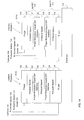
- FIG. 1A is a schematic view showing two exemplary thyristor detector devices integrated on a common substrate in accordance with the present invention.
- FIG. 1B is an energy band diagram of the thyristor detector devices of FIG. 1A .
- FIG. 2 illustrates an exemplary epitaxial growth structure utilizing group III-V materials for realizing the thyristor detector devices of FIGS. 1A and 1B in accordance with the present invention; other optoelectrical/electrical/optical devices can be monolithically integrated as part of this structure.
- FIG. 3A is a functional block diagram illustrating an exemplary embodiment of a thyristor detector device and supporting electronic circuitry in accordance with the present invention.
- FIG. 3B illustrates the operational characteristics of the thyristor detector device of FIG. 3A .
- FIG. 4 is a schematic diagram illustrating the system architecture of a High Angular Resolution Laser Irradiation Detector (HARLID) employing an array of thyristor detector devices in accordance with the present invention.
- HTLID High Angular Resolution Laser Irradiation Detector
- an array of thyristor radiation detectors includes complementary modulation doped quantum well interfaces formed between P+ layer(s) and N+ layer(s).
- each thyristor detector device is formed from a mesa that includes a refractory anode terminal formed adjacent the highly doped top P+ layer structure.
- a cathode terminal is operably coupled to a bottom N+ layer.
- An n-channel injector terminal and/or a p-channel injector terminal are operably coupled to the n-type and p-type modulation doped quantum well interfaces, respectively.
- the thyristor detector devices of the array operate over successive cycles each including a sequence of two distinct modes: a setup mode and a signal acquisition mode.
- a setup mode the n-type quantum well interface and/or the p-type quantum well interface is(are) substantially emptied of charge.
- Such operations reset the thyristor detector device into an OFF state if it was switched ON during the signal acquisition mode of the previous cycle.
- signal acquisition mode photocurrent is generated by the thyristor detector device in response to the absorption of incident electromagnetic radiation therein. The photocurrent can induce the thyristor detector device to switch from an OFF state to an ON state.
- the thyristor detector device Once switched into the ON state, the thyristor detector device remains in the ON state until it is reset in the setup mode of the next cycle.
- the OFF/ON state of the thyristor detector device at the end of signal acquisition mode produces an output digital electrical data that corresponds to the amount of incident radiation absorbed by the thyristor detector device during the signal acquisition mode of the current cycle.
- the n-type and p-type modulation doped quantum well interfaces of the thyristor devices of the array absorb electromagnetic radiation in the near-infrared range from 980 nm to 1650 nm and the undoped spacer layer disposed between the n-type and p-type modulation doped quantum well interfaces absorbs electromagnetic radiation in the visible range from 500 nm to 750 nm in addition to the near-infrared range from 750 nm to 980 nm, thus providing spectral sensitivity of the thyristor detector devices over a broad range from 500 nm to 1650 nm.
- the thyristor detector array of the present invention (and the signals produced therefrom) can be used in many applications. For example, it can be used as part of a High Angular Resolution Laser Irradiation Detector (HARLID) to detect the angle-of-arrival a collimated laser beam with high angular resolution.
- HTLID High Angular Resolution Laser Irradiation Detector
- the thyristor detector array of the present invention (and possibly other optoelectronic devices, logic circuits and/or signal processing circuits that are fabricated integral thereto) are realized from the inversion quantum-well channel device structures similar to those described in detail in U.S. Pat. No. 6,031,243; U.S. patent application Ser. No. 09/556,285, filed on Apr. 24, 2000; U.S. patent application Ser. No. 09/798,316, filed on Mar. 2, 2001; International Application No. PCT/US02/06802 filed on Mar. 4, 2002; U.S. patent application Ser. No. 08/949,504, filed on Oct. 14, 1997, U.S. patent application Ser. No. 10/200,967, filed on Jul.
- the essential features of this device structure include 1) an n-type modulation doped interface and a p-type modulation doped quantum well interface, 2) self-aligned n-type and p-type channel contacts formed by ion implantation, 3) n-type metal contacts to the n-type ion implants and the bottom n-type layer structure, and 4) p-type metal contacts to the p-type ion implants and the top p-type layer structure.
- the state of the charge in the n-type modulation doped quantum well interface and p-type modulation doped quantum well interface is controlled by conduction from either the anode or cathode as dictated by the bias conditions of the thyristor device.
- charge may be removed from the n-type modulation doped quantum well interface and p-type modulation doped quantum well interface by a current source (or pulse source) electrically coupled to the injector terminal for the respective interface.
- the metal anode is separated into two sections which are connected electrically by the P+ layer along the top surface ( FIG. 2 ). The active region of the device lies below the aperture formed by the two metal anode sections.
- FIG. 1A The structure of the two thyristor detector devices 101 A, 101 B is illustrated in FIG. 1A .
- FIG. 1B illustrates an exemplary energy band diagram for the thyristor detector devices 101 A, 101 B of FIG. 1A .
- the general layer structure of FIG. 1A can be configured to operate as a wide range of electronic devices (e.g., field effect transistors, bipolar transistors) such that these devices can be integrated to form a monolithic integrated circuit as described herein.
- the structure includes an active device structure which logically consists of two HFET devices. The first of these is a p-channel HFET device 111 (referred to herein as PHFET 111 ) comprising layers 114 , 116 , 118 , and 120 .
- PHFET 111 p-channel HFET device
- the PHFET device 111 which has a p-type modulation doped quantum well interface, is positioned with the gate terminal on the lower side and the collector terminal on the upper side.
- the second of these is an n-channel HFET device 113 (referred to herein as NHFET 113 ) comprising layers 120 , 122 , 124 , and 126 .
- the NHFET device 113 has an n-type modulation doped quantum well interface and is positioned with the gate terminal on the top side and the collector terminal on the lower side which is the collector of the p-channel device. Therefore a non-inverted n-channel device is stacked upon an inverted p-channel device to form the active device structure.
- n-type layer(s) 114 include a heavily doped layer that should not be depleted in any range of operation of the device, i.e. the total doping in this layer should exceed the total doping charge contained in the modulation doped layer of the p-type modulation doped quantum well interface 118 described below.
- Deposited on layer 114 is an undoped spacer layer 116 .
- Layers 114 and 116 serve electrically as part of the gate of the PHFET 111 . In this configuration, layer 114 achieves low contact resistance and layer 116 defines the capacitance of the PHFET 111 with respect to the p-type modulation doped quantum well interface 118 .
- a p-type modulation doped quantum well interface 118 that defines one or more quantum wells (which may be formed from strained or unstrained heterojunction materials) spaced apart from a p-type modulation doped layer.
- an undoped spacer layer 120 which forms the collector of the PHFET 111 . All of the layers grown thus far form the PHFET 111 with the gate ohmic contact on the bottom.
- Undoped spacer layer 120 forms the collector region of the NHFET 113 .
- Deposited on layer 120 is an n-type modulation doped quantum well interface 122 that defines one or more quantum wells (which may be formed from strained or unstrained heterojunction materials) spaced apart from an n-type modulation doped layer.
- Deposited on the n-type modulation doped quantum well interface 122 is an undoped spacer layer 124 .
- Deposited on layer 124 are p-type layer(s) 126 .
- the p-type layer(s) 126 include a heavily doped layer that should not be depleted in any range of operation of the device, i.e.
- the total doping in this layer should exceed the total doping charge contained in the modulation doped layer of the n-type modulation doped quantum well structure 122 described above.
- the p-type layer(s) 126 preferably include at least one layer which enables the formation of ohmic contacts thereto. In this configuration, layer(s) 126 achieves low contact resistance and layer 124 defines the capacitance of the NHFET 113 with respect to the n-type modulation doped quantum well interface 122 . Layers 124 , 126 and 128 serve as part of the gate of the NHFET 113 .
- the active device structure may be described as a pair of stacked quantum-well-base bipolar transistors formed on the substrate 110 .
- the first of these is an n-type quantum-well-base bipolar transistor (comprising layers 114 , 116 , 118 , and 120 ) which has one or more quantum wells spaced apart from a p-type modulation doped layer and is positioned with the emitter terminal on the lower side (i.e. on the mirror as just described) and the collector terminal on the upper side.
- the second of these is an n-type quantum-well-base bipolar transistor comprising layers 120 , 122 , 124 , and 126 .
- This n-type quantum-well-base bipolar transistor has one or more quantum wells spaced apart from an n-type modulation doped layer and is positioned with the emitter terminal on the top side and the collector terminal on the lower side (which is the collector of the p-type quantum-well-base bipolar transistor). Therefore a non-inverted n-channel device is stacked upon an inverted p-channel device to form the active device structure.
- the gate terminal of the p-channel HFET device 111 corresponds to the emitter terminal of the p-type quantum-well-base bipolar transistor
- the p-type quantum well interface 118 corresponds to the base region of the p-type quantum-well-base bipolar transistor
- spacer layer 120 corresponds to the collector region of both the p-type quantum-well-base bipolar transistor and the n-type quantum-well-base bipolar transistor
- the n-type quantum well interface 122 corresponds to the base region of the n-type quantum-well-base bipolar transistor
- the gate terminal of the n-channel HFET device 113 corresponds to the emitter electrode of the n-type quantum-well-base bipolar transistor.
- the thyristor detector devices 101 A, 101 B are adapted to perform a successive radiation detection cycles each including a setup mode and a signal acquisition mode.
- the n-type modulation doped quantum well interface 122 and the p-type quantum well interface 116 of the thyristor detector elements 101 A, 101 B are emptied of charge, thereby forcing both the n-type modulation doped quantum well interface 122 and the p-type quantum well interface 118 into a state of deep depletion.
- Such operations reset the thyristor detector device into an OFF state if it was switched ON during the signal acquisition mode of the previous cycle.
- this is accomplished by i) applying a current source to an n-channel injector terminal that contacts the n-type modulation doped quantum well interface 122 for emptying the n-type modulation doped quantum well interface 122 of free electrons, and ii) applying a current source to a p-channel injector terminal that contacts the p-type modulation doped quantum well interface 116 for emptying the p-type modulation doped quantum well interface 116 of free holes.
- electronic shutter control circuitry is preferably coupled to the cathode terminal electrode of the thyristor detector and maintains the cathode terminal electrode in a high impedance state (i.e., in other words the cathode terminal electrode floats) to disable induction from the cathode terminal.
- incident radiation is absorbed in both the n-type modulation doped quantum well interface 122 and the p-type modulation doped quantum well interface 118 of the thyristor detector device. Similar to the absorption process described in U.S. application Ser. No. 10/689,019, the absorbed radiation will empty the quantum well of the p-type quantum well interface 118 , thus accumulating positive charge in the p-type modulation doped layer and producing a forward bias on the p-type quantum well barrier, which results in a electron current flow over the p-type barrier to the n-type modulation doped quantum well interface 122 .
- Radiation absorbed in the n-type quantum well interface 122 will empty the quantum well of the interface 122 , thus accumulating negative charge in the n-type modulation doped layer and producing a forward bias on the n-type quantum well barrier, which results in a hole current flow over the n-type barrier to the p-type modulation doped quantum well interface 118 .
- the incident radiation can also be absorbed in the undoped spacer layer 120 of the thyristor detector device, which creates electrons and holes that are swept from the undoped spacer layer 20 by the built-in electric field between the n-type modulation doped quantum well interface 122 and the p-type modulation doped quantum well interface 118 .
- This field sweeps holes (i.e., hole current) toward the n-type modulation doped quantum well interface 122 and electrons (i.e., electron current) toward the p-type modulation doped quantum well interface 118 .
- the current caused by absorption of incident radiation can cause the thyristor detector device to switch from an OFF state (where substantially no current passes through the thyristor device from the anode terminal to the cathode terminal) to an ON state (where current passes through the thyristor device from the anode terminal to the cathode terminal).
- the thyristor detector device switches from the OFF state to the ON state in the even that photocurrent produces the critical switching charge Q CR in the n-type modulation doped quantum well interface 122 and/or the p-type modulation doped quantum well interface 118 .
- the sensitivity of the thyristor device in switching between states during the signal integration mode is preferably controlled by the supply of current to the n-type modulation doped quantum well interface 122 and/or to the p-type modulation doped quantum well interface 118 .
- the thyristor detector device Once switched into the ON state, the thyristor detector device remains in the ON state until it is reset in the setup mode of the next cycle.
- the OFF/ON state of the thyristor detector device at the end of signal acquisition mode produces an output digital electrical data that corresponds to the amount of incident radiation absorbed by the thyristor detector device during the signal acquisition mode for the current cycle.
- the radiation detection operations of the signal acquisition mode are accomplished by maintaining the voltage level at the anode terminal electrode at a positive voltage (e.g., on the order of three volts).
- electronic shutter circuitry coupled to the cathode terminal electrode of the thyristor detector device couples the cathode terminal electrode to ground through a bias resistance (not shown) to enable conduction from the cathode terminal.
- FIG. 2 illustrates an exemplary epitaxial growth structure utilizing group III-V materials for realizing the structure of FIG. 1A and electrical devices (e.g., HFET devices) formed from this structure in accordance with the present invention.
- group III-V materials such as a GaAs/AlGaAs.
- the structure of FIG. 2 can be made, for example, using known molecular beam epitaxy (MBE) techniques. As shown, the structure begins by depositing a layer 1114 of N+ type Al x2 Ga (1-x2) As upon a semi-insulating gallium arsenide substrate 1110 .
- the N+Al x2 Ga (1-x2) As layer 1114 should not be depleted in any range of operation of the device, i.e. the total doping in this layer should exceed the total doping charge contained in the modulation doped layer of the p-type modulation doped quantum well interface as described below.
- the parameter x 2 is preferably in the range between 70% and 80% (for example, on the order of 70%) for layer 1114 .
- Layer 1114 Deposited on layer 1114 are three layers 1116 , 1118 - 1 , 1118 - 2 of Al x1 Ga (1-x1) As.
- the parameter x 1 is preferably on the order of 15%.
- Layer 1116 is undoped and has a thickness on the order 300 ⁇ .
- Layers 1114 and 1116 serve as part of the gate of the PHFET 111 .
- Layer 1118 - 1 is doped P+ type in the form of delta doping and it forms the modulation doped layer of the p-type modulation doped quantum well interface 118 .
- Layer 1118 - 2 is undoped and forms a spacer layer between the modulation doped layer and the quantum wells of the p-typed modulation doped quantum well interface.
- the next layers define the quantum wells that form the inversion channel(s) during operation of the PHFET 111 , which include a quantum well layer 1118 - 3 A and a barrier layer 1118 - 3 B of undoped GaAs.
- the quantum well layer 1118 - 3 A may be comprised of a range of compositions.
- the quantum well is formed from an InGaAsN composition with the nitrogen content varying from 0% to 5% depending upon the desired wavelength of radiation that will be absorbed by the quantum well.
- the combination of the quantum well layer 1118 - 3 A and barrier layer 1118 - 3 B will typically be repeated (for example, 5 times), however single quantum well structures may also be used. Strained quantum well structures can also be used.
- the amount of nitrogen content for the respective quantum wells of the PHFET 111 dictates the bandgaps of such quantum wells and the radiation wavelengths that will be absorbed by such quantum wells.
- the nitrogen content (and corresponding bandgaps) of the respective quantum wells can be controlled to allow for absorption in the desired narrowband. For example, for sensitivity at a wavelength of 0.98 ⁇ m, the nitrogen content will be 0%; for sensitivity at a wavelength of 1.3 ⁇ m, the nitrogen content will be approximately 2%; and for sensitivity at a wavelength of 1.5 ⁇ m, the nitrogen content will be approximately 4%.
- the introduction of minute quantities of Sb is also helpful at the 1.5 ⁇ m wavelength to achieve high quality wells.
- sensitivity for any wavelength in the near-infrared range between 980 nm and 1650 nm may be realized.
- the nitrogen content (and corresponding bandgaps) of the respective quantum wells can be graded over the quantum wells to allow for sensitivity in the desired wavelength range.
- sensitivity for a range of near-infrared wavelengths between 980 nm and 1650 nm may be realized.
- a layer 1120 of undoped Al x1 Ga (1-x1) As which forms the collector of the PHFET device 111 and has a thickness on the order 3000 ⁇ . All of the layers grown thus far form the PHFET device 111 with the gate contact on the bottom.
- Undoped AlGaAs layer 1120 corresponds to the undoped spacer layer 120 of FIG. 1A .
- Layer 1120 also forms the collector region of the NHFET device 113 .
- Layer 1120 acts to absorb electromagnetic radiation preferably in the visible range between 500 nm to 750 nm as well as in the near-infrared range between 750 nm to 980 nm.
- Deposited on layer 1120 are layers that define the quantum wells that form the inversion channel(s) during operation of the NHFET 113 , which include a barrier layer 1122 - 1 A of undoped GaAs and a quantum well layer 1122 - 1 B.
- the quantum well layer 1122 - 1 B may be comprised of a range of compositions.
- the quantum well is formed from an InGaAsN composition with the nitrogen content varying from 0% to 5% depending upon the desired wavelength of radiation that will be absorbed by the quantum well.
- the combination of the barrier layer 1122 - 1 A and quantum well layer 1122 - 1 B will typically be repeated (for example, 5 times), however single quantum well structures may also be used. Strained quantum well structures can also be used.
- the amount of nitrogen content for the respective quantum wells of the NHFET 113 dictates the bandgaps of such quantum wells and the radiation wavelengths that will be absorbed by such quantum wells.
- the nitrogen content (and corresponding bandgaps) of the respective quantum wells can be controlled to allow for absorption in the desired narrowband. For example, for sensitivity at a wavelength of 0.98 ⁇ m, the nitrogen content will be 0%; for sensitivity at a wavelength of 1.3 ⁇ m, the nitrogen content will be approximately 2%; and for sensitivity at a wavelength of 1.5 ⁇ m, the nitrogen content will be approximately 4%.
- the introduction of minute quantities of Sb is also helpful at the 1.5 ⁇ m wavelength to achieve high quality wells.
- sensitivity for any wavelength in the near-infrared range between 980 nm and 1650 nm may be realized.
- the nitrogen content (and corresponding bandgaps) of the respective quantum wells can be graded over the quantum wells to allow for sensitivity in the desired wavelength range.
- the quantum wells of the NHFET 113 can have the largest bandgaps as compared to the quantum wells of the PHFET 111 , which can have the smallest bandgaps. This configuration provides for sensitivity of longer wavelength radiation in the quantum wells of the PHFET 111 as compared to the NHFET 113 which will have sensitivity to shorter wavelength radiation.
- the parameter x 1 is preferably on the order of 15%.
- Layer 1122 - 2 is undoped and forms a spacer layer between the quantum wells and the N+ modulation doped layer of the n-type modulation doped quantum well interface 122 .
- Layer 1122 - 3 is doped N+ type in the form of delta doping and it forms the modulation doped layer of the n-type modulation doped quantum well interface 122 .
- the doping species for layer 1122 - 2 is preferably carbon (C) to ensure diffusive stability.
- Layer 1124 is undoped and has a thickness on the order 300 ⁇ .
- the layers between the first barrier layer 1122 - 1 A and layer 1122 - 3 correspond to the n-type modulation doped quantum well interface 122 of FIG. 1A .
- Undoped AlGaAs layer 1124 corresponds to the undoped spacer layer 124 of FIG. 1A .
- Deposited on layer 1124 is a P+ type layer 1126 - 1 of Al x2 Ga (1-x2) As.
- the P+ type Al x2 Ga (1-x2) As layer 1126 - 1 is heavily doped such that it is not depleted in any range of operation of the device, i.e.
- a P+-type GaAs layer 1126 - 2 is deposited on the P+ type Al x2 Ga (1-x2) As layer 1126 - 1 .
- the P+ type GaAs layer 1126 - 2 enables the formation of ohmic contacts thereto.
- layer(s) 1126 - 2 achieves low contact resistance and layer 1126 - 1 defines the capacitance of the NHFET 113 with respect to the n-type modulation doped quantum well interface.
- Layers 1124 , 1126 - 1 and 1126 - 2 serve as part of the gate of the NHFET 113 .
- the active device structure may be described as a pair of stacked quantum-well-base bipolar transistors formed on the substrate 1110 .
- the first of these is a p-type quantum-well-base bipolar transistor (comprising layers 1114 through 1120 ) which has one or more p-type modulation doped quantum wells and is positioned with the emitter terminal on the lower side (i.e. on the bottom mirror as just described) and the collector terminal on the upper side.
- the second of these is an n-type quantum-well-base bipolar transistor (comprising layers 1120 through 1126 - 2 ) which has one or more n-type modulation doped quantum wells and is positioned with the emitter terminal on the top side and the collector terminal on the lower side which is the collector of the p-type quantum-well-base bipolar transistor. Therefore a non-inverted n-channel device is stacked upon an inverted p-channel device to form the active device structure.
- the cathode terminal of the thyristor device corresponds to the emitter electrode of the p-type quantum-well-base bipolar transistor
- the p-type quantum well structure (layers 1118 - 1 though 1118 - 3 B) corresponds to the base region of the p-type quantum-well-base bipolar transistor
- spacer layer 1120 corresponds to the collector region of both the p-type quantum-well-base bipolar transistor and the n-type quantum-well-base bipolar transistor
- the n-type quantum well structure (layers 1122 - 1 A through 1122 - 3 ) corresponds to the base region of the n-type quantum-well-base bipolar transistor
- the anode terminal of the thyristor device correspond to the emitter electrode of the n-type quantum-well-base bipolar transistor.
- the structure of FIG. 2 may also be used to realize various electronic devices, including transistor devices (such as n-channel HFET devices, p-channel HFET devices, n-type quantum-well-base bipolar transistors and p-type quantum-well-base bipolar transistors).
- transistor devices such as n-channel HFET devices, p-channel HFET devices, n-type quantum-well-base bipolar transistors and p-type quantum-well-base bipolar transistors.
- Such devices are similar to those described in detail in U.S. patent application Ser. No. 10/323,388, filed on Dec. 19, 2002; and U.S. patent application Ser. No. 10/340,942, filed on Jan. 13, 2003; incorporated by reference above in their entireties.
- alignment marks are defined by etching, and then a layer of Si 3 N 4 or Al 2 O 3 or other suitable dielectric (not shown) is deposited to act as protection for the surface layer and as a blocking layer for subsequent ion implants.
- the refractory anode terminals 136 A and 136 B of the thyristor detector devices are deposited and defined preferably via liftoff of metal.
- mesas are formed to define the active areas for the thyristor detector devices of the array.
- the active area for a given thyristor detector elements is located under the aperture between the anode terminals 136 A, 136 B of the given thyristor detector element as shown in FIG. 2 .
- the active area mesas are formed by etching down to (or near) N+ type layer 1122 - 3 .
- an ion implant 171 of N+ type is performed using a photomask that is aligned to the alignments marks to implant n-type ions into the n-type modulation doped quantum well interface of the thyristor detector devices, to thereby form contacts to the n-type modulation doped quantum well interface for the thyristor detector elements.
- the implant 171 is subsequently metallized as described below to form n-channel injector terminals 137 A, 137 B for the respective thyristor detector device as shown in FIG. 2 .
- an ion implant 172 of P+ type is performed using a photomask that is aligned to the alignments marks to implant p-type ions into the p-type modulation doped quantum well interface of the thyristor detector devices, to thereby form contacts to the p-type modulation doped quantum well interface for the thyristor detector elements.
- mesas are formed by etching preferably down to the spacer layer 1120 .
- the resulting mesas are then subject to P+ ion implant 172 .
- the implant 172 is subsequently metallized as described below to form p-channel injector terminals 138 A, 138 B for the respective thyristor detector device as shown in FIG. 2 .
- connection of the cathode of the thyristor-based pixel elements is made by etching down near the N+ type layer 1114 .
- the exposed portion of the mesa near the N+ type layer 1114 is subsequently metallized as described below to form cathode terminals 139 A, 139 B for the respective thyristor detector device as shown in FIG. 2 .
- the thyristor detector devices are subjected to a rapid thermal anneal (RTA) of the order of 900° C. or greater to activate all implants. Then the thyristor detector devices are isolated from one another by etching down to the semi-insulating substrate 1110 . Note that etch down to the semi-insulating substrate 1110 can be omitted. In this scenario, isolation can be provided by an ion implant (for example, O 2 ions).
- RTA rapid thermal anneal
- the next step in the fabrication is the deposition (preferably via lift off) of metal contacts. These contacts come in three forms. One is a metal layer (preferably comprising an n-type Au alloy metal such as AuGe/Ni/Au) that forms the cathode terminal electrodes 139 A, 129 B as shown in FIG. 2 . The second is a metal layer (preferably comprising a p-type Au metal alloy such as AuZn/Cr/Au) deposited on the P+ type implant 172 to form the p-channel injector terminal electrodes 138 A, 138 B as shown in FIG. 2 .
- a metal layer preferably comprising an n-type Au alloy metal such as AuGe/Ni/Au
- the second is a metal layer (preferably comprising a p-type Au metal alloy such as AuZn/Cr/Au) deposited on the P+ type implant 172 to form the p-channel injector terminal electrodes 138 A, 138 B as shown in FIG. 2 .
- the third is the metal layer (preferably comprising an n-type Au alloy metal such as AuGe/Ni/Au) deposited on the N+ type implant 171 to form the n-channel injector terminal electrodes 137 A, 137 B as shown in FIG. 2 .
- the metallization of the cathode terminal electrodes and the n-channel injector terminal electrodes is performed as a single lift-off operation.
- the GaAs substrate 1110 can be doped N+ and thus intrinsically realize the N+ type layer 1114 .
- connection to the N+substrate 1110 of the cathode can be made on the bottom side of the N+substrate 1110 by metallization thereon. Isolation can be provided by an ion implant (for example, O 2 ions).
- the thyristor detector device of FIG. 2 is adapted to operate over successive cycles each including a sequence of two distinct modes: a setup mode and a signal acquisition mode.
- a setup mode the n-type quantum well interface 122 and/or the p-type quantum well interface 118 is(are) substantially emptied of charge.
- Such operations reset the thyristor detector device into an OFF state if it was switched ON during the signal acquisition mode of the previous cycle.
- photocurrent is generated by the thyristor detector device in response to the absorption of incident electromagnetic radiation therein. The photocurrent can induce the thyristor detector device to switch from an OFF state to an ON state.
- the thyristor detector device Once switched into the ON state, the thyristor detector device remains in the ON state until it is reset in the setup mode of the next cycle.
- the OFF/ON state of the thyristor detector device at the end of signal acquisition mode produces an output digital electrical data that corresponds to the amount of incident radiation absorbed by the thyristor detector device during the signal acquisition mode of the current cycle.
- the n-type and p-type modulation doped quantum well interfaces 122 , 118 of the thyristor devices of the array absorb electromagnetic radiation in the near-infrared range from 980 nm to 1650 nm and the undoped spacer layer 120 disposed between the n-type and p-type modulation doped quantum well interfaces absorbs electromagnetic radiation in the visible range from 500 nm to 750 nm in addition to the near-infrared range from 750 nm to 980 nm, thus providing spectral sensitivity of the thyristor detector devices over a broad range from 500 nm to 1650 nm.
- FIGS. 3A and 3B illustrate the operational characteristics of the thyristor detector device of FIGS. 1A , 1 B and 2 .
- the thyristor detector device 101 switches from a non-conducting/OFF state (where the current I LOAD is substantially zero) to a conducting/ON state (where current I LOAD is substantially greater than zero) when: i) the anode terminal electrode (A) is forward biased (e.g.
- the critical switching charge Q CR is unique to the geometries and doping levels of the device.
- the switching voltage of the device i.e., the voltage that provides the critical switching charge Q CR ) varies over the p-channel injector current I g — p and the n-channel injector current I g — n, collectively referred to as I g , as shown in FIG. 3B .
- the device switches from the conducting/ON state (where the current I LOAD is substantially greater than zero) to a non-conducting/OFF state (where current I LOAD is substantially zero) when the current I LOAD through the device falls below the hold current I H of the device for a sufficient period of time such that the charge in the n-type modulation doped quantum well interface 122 and/or the p-type modulation doped quantum well interface 118 decreases below the holding charge Q H , which is the critical value of the channel charge which will sustain holding action.
- the anode terminal electrode (A), which corresponds to the anode terminal electrodes 136 A, 136 B of FIG. 2 is forward biased (e.g. biased positively) with respect to the cathode terminal electrode (C), which corresponds to the cathode terminal electrodes 139 A, 139 B of FIG. 2 .
- Bias Current Source 20 A provides a bias current I OUT — N that draws charge (e.g., electrons) from the n-type modulation doped quantum well interface 122 electrically connected to the n-channel injector terminal electrode ( 138 A, 138 B).
- Bias Current Source 20 B provides a bias current I IN — N that injects charge (e.g., electrons) into the n-type modulation doped quantum well interface 122 electrically connected to the n-channel injector terminal electrode ( 138 A, 138 B).
- Bias Current Source 20 C provides a bias current I OUT — P that draws charge (e.g., holes) from the p-type modulation doped quantum well interface 118 electrically connected to the p-channel injector terminal electrode ( 139 A, 138 B).
- Bias Current Source 20 D provides a bias current I IN — P that injects charge (e.g., holes) into the p-type modulation doped quantum well interface 118 electrically connected to the p-channel injector terminal electrode ( 139 A, 138 B).
- charge e.g., holes
- bias current source 20 A is providing an electron current I OUT — N drawing on the n-channel injector terminal electrode
- the absorption of incident radiation can produce photocurrent in excess of such electron current. In the event that such excess photocurrent produces the critical switching charge Q CR in the n-type modulation doped quantum well interface 122 , the thyristor device will switch to its ON state.
- bias current source 20 B is providing an electron current I IN — N supplied to the n-channel injector terminal electrode
- the absorption of incident radiation can produce photocurrent that sums with the bias current I IN — N . In the event that such current sum produces the critical switching charge Q CR in the n-type modulation doped quantum well interface 122 , the thyristor device will switch to its ON state.
- bias current source 20 C is providing a hole current I OUT — P drawing on the p-channel injector terminal electrode
- the absorption of incident radiation can produce photocurrent in excess of such hole current.
- the critical switching charge Q CR in the p-type modulation doped quantum well interface 118 the thyristor device will switch to its ON state.
- bias current source 20 D is providing an electron current I IN — P supplied to the p-channel injector terminal electrode
- the absorption of incident radiation can produce photocurrent that sums with the bias current I IN — P .
- the thyristor device will switch to its ON state.
- a load bias resistance R BD dictates the load current I DON in the ON state and the load current I DOFF in the OFF state.
- the load bias resistance R BD provides a load current I DON in the ON state well above the hold current (I H ) and a load current I DOFF in the OFF state well below the hold current (I H ) as shown.
- an output digital electrical signal whose logic level represents the detection (or non-detection) of incident radiation over the signal acquisition mode of the current cycle is generated at the cathode terminal electrode of the thyristor detector device.
- the transistor J 1 operates as an electronic shutter that selectively couples and decoupled the cathode terminal electrode to ground through the bias load resistance R B , to thereby enable and disable conduction from the cathode terminal.
- the transistor J 1 is switched ON to selectively couple the cathode terminal electrode to ground through the bias load resistance R B , to thereby enable conduction from the cathode terminal.
- the transistor J 1 is switched OFF to selectively decouple the cathode terminal electrode to ground through the bias load resistance R B , to thereby disable conduction from the cathode terminal.
- the bias current source 20 A is operated to draw charge (electrons) from the n-type modulation doped quantum well interface 122 in order to empty it of free electrons.
- the bias current source 20 C is operated to draw charge (holes) from the p-type modulation doped quantum well interface 118 in order to empty it of free holes.
- bias current sources 20 A, 20 B, 20 C and 20 D are optional and the amount of bias current supplied by such bias current sources (if any) provide for control over the sensitivity of the detection operations of the thyristor detector device during the signal acquisition mode of each cycle. It is contemplated that the bias current sources can be realized by electrically-controlled bias current circuitry (e.g., voltage-controlled bias current source circuitry, current-controlled bias current source circuitry, etc.) that can be selectively activated and controlled by electrical signals supplied thereto.
- electrically-controlled bias current circuitry e.g., voltage-controlled bias current source circuitry, current-controlled bias current source circuitry, etc.
- FIG. 4 illustrates an array of thyristor detector devices ( 101 A, 101 B, . . . 101 N) that are fabricated on a substrate 110 as part of a monolithic integrated circuit for high angular resolution laser irradiation detection (HARLID).
- a mask 151 is provided that blocks incident radiation within the spectral range of interest (e.g., between 500 nm and 1650 nm).
- the mask 151 includes multiple apertures positioned above the array of thyristor detector devices ( 101 A, 101 B, . . . 101 N).
- the apertures allow the incident radiation to pass through the mask 151 to the thyristor detector devices ( 101 A, 101 B, . . . 101 N), which are adapted to perform successive radiation detection cycles each including a setup mode and a signal acquisition mode as described herein.
- the outputs of the thyristor detector devices ( 101 A, 101 B, . . . 101 N) are supplied to decode logic 155 via corresponding transmission gates ( 153 A, 153 B, . . . 153 N).
- the angle-of-arrival ( ⁇ i ) of the incident laser beam is determined by the decode logic 155 from the output signals of the thyristor detector devices ( 101 A, 101 B, . . . 101 N) and the areas where the apertures of the mask 151 are imaged onto the thyristor detector devices ( 101 A, 101 B, . . . 101 N) as is well known in the art.
- the decode logic 155 is preferably realized by HFET transistor devices that are integrally formed on the substrate 110 .
- the mask 151 can be integrally formed on the substrate 110 as part of the monolithic integrated circuit (preferably by material deposition and etching of the apertures of the mask 151 ). It is also contemplated that an antireflective coating can cover the apertures of the mask 151 as is well known in the art.
- the n-type and p-type modulation doped quantum well interfaces 122 , 118 of the thyristor devices of the array absorb electromagnetic radiation in the near-infrared range from 980 nm to 1650 nm and the undoped spacer layer 120 disposed between the n-type and p-type modulation doped quantum well interfaces absorbs electromagnetic radiation in the visible range from 500 nm to 750 nm in addition to the near-infrared range from 750 nm to 980 nm, thus providing spectral sensitivity of the thyristor detector devices over a broad range from 500 nm to 1650 nm.
- the thyristor detectors of the array can be arranged as a linear array (with a constant active area size over the thyristor detector devices of the array) positioned under a mask comprising a plurality of two-dimensional apertures (where size of the apertures vary over rows of such apertures).
- the thyristor detectors of the array can be arranged as a two dimensional array of thyristor detector devices with variable active area size over the thyristor detector devices of the two dimensional array.
- the thyristor detector devices are positioned under a linear shadow mask with a single slot aperture that allows incident radiation to pass to the thyristor detector devices.
- the angle-of-arrival ( ⁇ i ) of the incident laser beam is determined by decode logic from the output signals of the variable size thyristor detector devices as is well known in the art.
- the thyristor detectors of the array, the mask and the decode logic of the HARLID of FIG. 4 can be arranged to measure angle-of-arrival in two orthogonal directions.
- the sensitivity of the thyristor detector devices can be adjusted over successive images cycles in order to detect high power sources as well as lower power sources.
- the system can detect the time-to-switch period (i.e., the time period from the start of the signal acquisition mode to the time that the thyristor switches ON, if any) for the thyristor detector devices of the array.
- This time-to-switch period can be used to adjust the bias current applied to the modulation doped quantum well interfaces of the device. For example, if the time-to-switch is less than a predetermined minimum time period, the bias currents can be adjusted to reduce the sensitivity of the thyristor detector devices of the array. Alternatively, if the time-to-switch is greater than a predetermined maximum time period (or does not occur at all), the bias currents can be adjusted to increase the sensitivity of the thyristor detector devices of the array.
- the thyristor detector devices as described herein can be fabricated within an integrally formed resonant cavity for increased sensitivity.
- a bottom distributed reflective mirror is formed on the substrate under the active device structure.
- a top dielectric mirror is formed over the p-type layer(s) of the device.
- Incident radiation enters the resonant cavity in a vertical direction through an optical aperture (not shown) in the top surface (or bottom surface) of the device.
- the optical path length between the bottom DBR mirror and top dielectric mirror preferably represents an integral number of 1 ⁇ 2 wavelengths at the designated wavelength. Preferably, this optical path length is controlled by adjusting the thickness of one or more of the layers therebetween to enable this condition.
Abstract
Description
Claims (28)
Priority Applications (2)
| Application Number | Priority Date | Filing Date | Title |
|---|---|---|---|
| US12/050,321 US8080821B2 (en) | 2008-03-18 | 2008-03-18 | Thyristor radiation detector array and applications thereof |
| EP09250751.6A EP2104146A3 (en) | 2008-03-18 | 2009-03-18 | Thyristor radiation detector array and applications thereof |
Applications Claiming Priority (1)
| Application Number | Priority Date | Filing Date | Title |
|---|---|---|---|
| US12/050,321 US8080821B2 (en) | 2008-03-18 | 2008-03-18 | Thyristor radiation detector array and applications thereof |
Publications (2)
| Publication Number | Publication Date |
|---|---|
| US20100123121A1 US20100123121A1 (en) | 2010-05-20 |
| US8080821B2 true US8080821B2 (en) | 2011-12-20 |
Family
ID=40637151
Family Applications (1)
| Application Number | Title | Priority Date | Filing Date |
|---|---|---|---|
| US12/050,321 Active 2030-06-04 US8080821B2 (en) | 2008-03-18 | 2008-03-18 | Thyristor radiation detector array and applications thereof |
Country Status (2)
| Country | Link |
|---|---|
| US (1) | US8080821B2 (en) |
| EP (1) | EP2104146A3 (en) |
Cited By (1)
| Publication number | Priority date | Publication date | Assignee | Title |
|---|---|---|---|---|
| US9276160B2 (en) | 2014-05-27 | 2016-03-01 | Opel Solar, Inc. | Power semiconductor device formed from a vertical thyristor epitaxial layer structure |
Families Citing this family (10)
| Publication number | Priority date | Publication date | Assignee | Title |
|---|---|---|---|---|
| US9517023B2 (en) | 2009-06-01 | 2016-12-13 | Profusa, Inc. | Method and system for directing a localized biological response to an implant |
| US10010272B2 (en) | 2010-05-27 | 2018-07-03 | Profusa, Inc. | Tissue-integrating electronic apparatus |
| CN110604585B (en) | 2010-10-06 | 2023-04-18 | 普罗弗萨股份有限公司 | Tissue-integrating sensor |
| US10045722B2 (en) | 2013-03-14 | 2018-08-14 | Profusa, Inc. | Method and device for correcting optical signals |
| CN111544011B (en) * | 2013-06-06 | 2023-06-06 | 普罗菲尤萨股份有限公司 | Apparatus and method for detecting optical signals from implanted sensors |
| US9590742B2 (en) * | 2014-12-22 | 2017-03-07 | Opel Solar, Inc. | Thyristor-based optical XOR circuit |
| US20190145926A1 (en) * | 2016-04-29 | 2019-05-16 | Stc. Unm | Wafer level gate modulation enhanced detectors |
| WO2018119400A1 (en) | 2016-12-22 | 2018-06-28 | Profusa, Inc. | System and single-channel luminescent sensor for and method of determining analyte value |
| CN108075749A (en) * | 2017-12-19 | 2018-05-25 | 中国工程物理研究院流体物理研究所 | High pressure photoimpact thyristor and its Triggering Control System and its trigger control method |
| CN110444628B (en) * | 2018-05-04 | 2021-11-09 | 中国科学院苏州纳米技术与纳米仿生研究所 | Infrared detector and manufacturing method thereof |
Citations (3)
| Publication number | Priority date | Publication date | Assignee | Title |
|---|---|---|---|---|
| US5604695A (en) * | 1995-06-05 | 1997-02-18 | Her Majesty The Queen, As Represented By The Minister Of National Defence Of Her Majesty's Canadian Government | Analog high resolution laser irradiation detector (HARLID) |
| US20040079971A1 (en) * | 2000-04-24 | 2004-04-29 | The University Of Connecticut | Imaging array utilizing thyristor-based pixel elements |
| US7012274B2 (en) | 2001-03-02 | 2006-03-14 | The University Of Connecticut | Modulation doped thyristor and complementary transistors combination for a monolithic optoelectronic integrated circuit |
Family Cites Families (2)
| Publication number | Priority date | Publication date | Assignee | Title |
|---|---|---|---|---|
| US6031243A (en) | 1996-10-16 | 2000-02-29 | Geoff W. Taylor | Grating coupled vertical cavity optoelectronic devices |
| DE10218160C1 (en) * | 2002-04-23 | 2003-12-24 | Elmos Semiconductor Ag | Device for determining the angle of incidence of radiation on a radiation incidence surface |
-
2008
- 2008-03-18 US US12/050,321 patent/US8080821B2/en active Active
-
2009
- 2009-03-18 EP EP09250751.6A patent/EP2104146A3/en not_active Withdrawn
Patent Citations (3)
| Publication number | Priority date | Publication date | Assignee | Title |
|---|---|---|---|---|
| US5604695A (en) * | 1995-06-05 | 1997-02-18 | Her Majesty The Queen, As Represented By The Minister Of National Defence Of Her Majesty's Canadian Government | Analog high resolution laser irradiation detector (HARLID) |
| US20040079971A1 (en) * | 2000-04-24 | 2004-04-29 | The University Of Connecticut | Imaging array utilizing thyristor-based pixel elements |
| US7012274B2 (en) | 2001-03-02 | 2006-03-14 | The University Of Connecticut | Modulation doped thyristor and complementary transistors combination for a monolithic optoelectronic integrated circuit |
Cited By (1)
| Publication number | Priority date | Publication date | Assignee | Title |
|---|---|---|---|---|
| US9276160B2 (en) | 2014-05-27 | 2016-03-01 | Opel Solar, Inc. | Power semiconductor device formed from a vertical thyristor epitaxial layer structure |
Also Published As
| Publication number | Publication date |
|---|---|
| US20100123121A1 (en) | 2010-05-20 |
| EP2104146A2 (en) | 2009-09-23 |
| EP2104146A3 (en) | 2017-05-17 |
Similar Documents
| Publication | Publication Date | Title |
|---|---|---|
| US8080821B2 (en) | Thyristor radiation detector array and applications thereof | |
| US9768211B2 (en) | Integrated avalanche photodiode arrays | |
| US7262429B2 (en) | Thz detection employing modulation doped quantum well device structures | |
| US7432539B2 (en) | Imaging method utilizing thyristor-based pixel elements | |
| US6794631B2 (en) | Three-terminal avalanche photodiode | |
| US6841795B2 (en) | Semiconductor devices employing at least one modulation doped quantum well structure and one or more etch stop layers for accurate contact formation | |
| Liu et al. | A planar InP/InGaAs avalanche photodiode with floating guard ring and double diffused junction | |
| US6870207B2 (en) | III-V charge coupled device suitable for visible, near and far infra-red detection | |
| KR100912358B1 (en) | A modulation doped thyristor and complementary transistor combination for a monolithic optoelectronic integrated circuit | |
| US9041136B2 (en) | Avalanche photodiode | |
| US6954473B2 (en) | Optoelectronic device employing at least one semiconductor heterojunction thyristor for producing variable electrical/optical delay | |
| US8314446B2 (en) | Photo-detector array, semiconductor image intensifier and methods of making and using the same | |
| CA2969509C (en) | Avalanche photodiode | |
| US7556976B2 (en) | Method of fabricating semiconductor devices employing at least one modulation doped quantum well structure and one or more etch stop layers for accurate contact formation | |
| US10944021B2 (en) | Virtual negative bevel and methods of isolating adjacent devices | |
| EP2446483A1 (en) | Low-level signal detection by semiconductor avalanche amplification | |
| US7776753B2 (en) | Method of fabricating semiconductor devices employing at least one modulation doped quantum well structure and one or more etch stop layers for accurate contact formation | |
| US11520014B2 (en) | Thyristor-based lidar detector array | |
| US7385230B1 (en) | Modulation doped thyristor and complementary transistor combination for a monolithic optoelectronic integrated circuit | |
| US7015120B2 (en) | Method of fabricating semiconductor devices employing at least one modulation doped quantum well structure and one or more etch stop layers for accurate contact formation | |
| WO2004038765A2 (en) | Optoelectronic clock generator and other optoelectronic devices and systems employing at least one heterojunction thyristor device | |
| Berger | Metal-semiconductor-metal photodetectors | |
| JPH09199753A (en) | Super-lattice avalanche photodiode | |
| WO2004038764A2 (en) | Semiconductor device with quantum well and etch stop |
Legal Events
| Date | Code | Title | Description |
|---|---|---|---|
| AS | Assignment |
Owner name: CONNECTICUT, THE UNIVERSITY OF,CONNECTICUT Free format text: ASSIGNMENT OF ASSIGNORS INTEREST;ASSIGNOR:TAYLOR, GEOFF W.;REEL/FRAME:020695/0544 Effective date: 20080308 Owner name: OPEL, INC.,CONNECTICUT Free format text: ASSIGNMENT OF ASSIGNORS INTEREST;ASSIGNOR:TAYLOR, GEOFF W.;REEL/FRAME:020695/0544 Effective date: 20080308 Owner name: CONNECTICUT, THE UNIVERSITY OF, CONNECTICUT Free format text: ASSIGNMENT OF ASSIGNORS INTEREST;ASSIGNOR:TAYLOR, GEOFF W.;REEL/FRAME:020695/0544 Effective date: 20080308 Owner name: OPEL, INC., CONNECTICUT Free format text: ASSIGNMENT OF ASSIGNORS INTEREST;ASSIGNOR:TAYLOR, GEOFF W.;REEL/FRAME:020695/0544 Effective date: 20080308 |
|
| STCF | Information on status: patent grant |
Free format text: PATENTED CASE |
|
| AS | Assignment |
Owner name: TCA GLOBAL CREDIT MASTER FUND, LP, FLORIDA Free format text: SECURITY AGREEMENT;ASSIGNOR:OPEL SOLAR, INC.;REEL/FRAME:028350/0244 Effective date: 20120330 |
|
| AS | Assignment |
Owner name: OPEL SOLAR, INC., CONNECTICUT Free format text: CHANGE OF NAME;ASSIGNOR:OPEL INC.;REEL/FRAME:029426/0350 Effective date: 20111026 |
|
| AS | Assignment |
Owner name: OPEL SOLAR, INC., CONNECTICUT Free format text: RELEASE BY SECURED PARTY;ASSIGNOR:TCA GLOBAL CREDIT MASTER FUND, LP;REEL/FRAME:029437/0950 Effective date: 20121205 |
|
| FPAY | Fee payment |
Year of fee payment: 4 |
|
| AS | Assignment |
Owner name: ESPRESSO CAPITAL LTD., CANADA Free format text: SECURITY INTEREST;ASSIGNOR:OPEL INC.;REEL/FRAME:048886/0716 Effective date: 20190326 |
|
| AS | Assignment |
Owner name: ESPRESSO CAPITAL LTD., CANADA Free format text: CORRECTIVE ASSIGNMENT TO CORRECT THE EXECUTION DATE PREVIOUSLY RECORDED AT REEL: 048886 FRAME: 0716. ASSIGNOR(S) HEREBY CONFIRMS THE SECURITY INTEREST;ASSIGNOR:BB PHOTONICS INC.;REEL/FRAME:048947/0480 Effective date: 20190418 |
|
| FEPP | Fee payment procedure |
Free format text: 7.5 YR SURCHARGE - LATE PMT W/IN 6 MO, SMALL ENTITY (ORIGINAL EVENT CODE: M2555); ENTITY STATUS OF PATENT OWNER: SMALL ENTITY |
|
| MAFP | Maintenance fee payment |
Free format text: PAYMENT OF MAINTENANCE FEE, 8TH YR, SMALL ENTITY (ORIGINAL EVENT CODE: M2552); ENTITY STATUS OF PATENT OWNER: SMALL ENTITY Year of fee payment: 8 |
|
| AS | Assignment |
Owner name: OPEL INC., CALIFORNIA Free format text: RELEASE BY SECURED PARTY;ASSIGNOR:ESPRESSO CAPITAL LTD.;REEL/FRAME:051069/0619 Effective date: 20191107 |
|
| MAFP | Maintenance fee payment |
Free format text: PAYMENT OF MAINTENANCE FEE, 12TH YR, SMALL ENTITY (ORIGINAL EVENT CODE: M2553); ENTITY STATUS OF PATENT OWNER: SMALL ENTITY Year of fee payment: 12 |