US8079667B2 - Drop generating apparatus - Google Patents
Drop generating apparatus Download PDFInfo
- Publication number
- US8079667B2 US8079667B2 US12/338,169 US33816908A US8079667B2 US 8079667 B2 US8079667 B2 US 8079667B2 US 33816908 A US33816908 A US 33816908A US 8079667 B2 US8079667 B2 US 8079667B2
- Authority
- US
- United States
- Prior art keywords
- drop generator
- insulating layer
- electrically insulating
- electrically
- conductive layer
- Prior art date
- Legal status (The legal status is an assumption and is not a legal conclusion. Google has not performed a legal analysis and makes no representation as to the accuracy of the status listed.)
- Expired - Fee Related, expires
Links
- 239000000758 substrate Substances 0.000 claims description 23
- 238000000576 coating method Methods 0.000 claims description 8
- 229910052751 metal Inorganic materials 0.000 claims description 7
- 239000002184 metal Substances 0.000 claims description 7
- 229920000052 poly(p-xylylene) Polymers 0.000 claims description 7
- 239000004593 Epoxy Substances 0.000 claims description 4
- 239000011248 coating agent Substances 0.000 claims description 4
- -1 polytetrafluorethylene Polymers 0.000 claims description 4
- 229920001343 polytetrafluoroethylene Polymers 0.000 claims description 3
- 229920002635 polyurethane Polymers 0.000 claims description 3
- 239000004814 polyurethane Substances 0.000 claims description 3
- 229910044991 metal oxide Inorganic materials 0.000 claims 2
- 150000004706 metal oxides Chemical class 0.000 claims 2
- 239000010408 film Substances 0.000 description 9
- 239000012530 fluid Substances 0.000 description 9
- 238000000034 method Methods 0.000 description 8
- 238000002048 anodisation reaction Methods 0.000 description 4
- 238000010586 diagram Methods 0.000 description 4
- TWNQGVIAIRXVLR-UHFFFAOYSA-N oxo(oxoalumanyloxy)alumane Chemical compound O=[Al]O[Al]=O TWNQGVIAIRXVLR-UHFFFAOYSA-N 0.000 description 4
- 239000010409 thin film Substances 0.000 description 4
- 239000007788 liquid Substances 0.000 description 3
- 239000000463 material Substances 0.000 description 3
- 150000002739 metals Chemical class 0.000 description 3
- PXHVJJICTQNCMI-UHFFFAOYSA-N Nickel Chemical compound [Ni] PXHVJJICTQNCMI-UHFFFAOYSA-N 0.000 description 2
- VYPSYNLAJGMNEJ-UHFFFAOYSA-N Silicium dioxide Chemical compound O=[Si]=O VYPSYNLAJGMNEJ-UHFFFAOYSA-N 0.000 description 2
- 229910052782 aluminium Inorganic materials 0.000 description 2
- XAGFODPZIPBFFR-UHFFFAOYSA-N aluminium Chemical compound [Al] XAGFODPZIPBFFR-UHFFFAOYSA-N 0.000 description 2
- 239000003990 capacitor Substances 0.000 description 2
- 238000005260 corrosion Methods 0.000 description 2
- 230000007797 corrosion Effects 0.000 description 2
- 238000005553 drilling Methods 0.000 description 2
- 238000007747 plating Methods 0.000 description 2
- 238000007639 printing Methods 0.000 description 2
- 238000007789 sealing Methods 0.000 description 2
- 229910001220 stainless steel Inorganic materials 0.000 description 2
- 239000010935 stainless steel Substances 0.000 description 2
- 229910052715 tantalum Inorganic materials 0.000 description 2
- GUVRBAGPIYLISA-UHFFFAOYSA-N tantalum atom Chemical compound [Ta] GUVRBAGPIYLISA-UHFFFAOYSA-N 0.000 description 2
- BTBUEUYNUDRHOZ-UHFFFAOYSA-N Borate Chemical compound [O-]B([O-])[O-] BTBUEUYNUDRHOZ-UHFFFAOYSA-N 0.000 description 1
- RYGMFSIKBFXOCR-UHFFFAOYSA-N Copper Chemical compound [Cu] RYGMFSIKBFXOCR-UHFFFAOYSA-N 0.000 description 1
- FEWJPZIEWOKRBE-JCYAYHJZSA-N Dextrotartaric acid Chemical compound OC(=O)[C@H](O)[C@@H](O)C(O)=O FEWJPZIEWOKRBE-JCYAYHJZSA-N 0.000 description 1
- FYYHWMGAXLPEAU-UHFFFAOYSA-N Magnesium Chemical compound [Mg] FYYHWMGAXLPEAU-UHFFFAOYSA-N 0.000 description 1
- NBIIXXVUZAFLBC-UHFFFAOYSA-N Phosphoric acid Chemical compound OP(O)(O)=O NBIIXXVUZAFLBC-UHFFFAOYSA-N 0.000 description 1
- 229910052581 Si3N4 Inorganic materials 0.000 description 1
- BQCADISMDOOEFD-UHFFFAOYSA-N Silver Chemical compound [Ag] BQCADISMDOOEFD-UHFFFAOYSA-N 0.000 description 1
- QAOWNCQODCNURD-UHFFFAOYSA-N Sulfuric acid Chemical compound OS(O)(=O)=O QAOWNCQODCNURD-UHFFFAOYSA-N 0.000 description 1
- GWEVSGVZZGPLCZ-UHFFFAOYSA-N Titan oxide Chemical compound O=[Ti]=O GWEVSGVZZGPLCZ-UHFFFAOYSA-N 0.000 description 1
- RTAQQCXQSZGOHL-UHFFFAOYSA-N Titanium Chemical compound [Ti] RTAQQCXQSZGOHL-UHFFFAOYSA-N 0.000 description 1
- NRTOMJZYCJJWKI-UHFFFAOYSA-N Titanium nitride Chemical compound [Ti]#N NRTOMJZYCJJWKI-UHFFFAOYSA-N 0.000 description 1
- HCHKCACWOHOZIP-UHFFFAOYSA-N Zinc Chemical compound [Zn] HCHKCACWOHOZIP-UHFFFAOYSA-N 0.000 description 1
- 238000007743 anodising Methods 0.000 description 1
- 238000005452 bending Methods 0.000 description 1
- 230000009286 beneficial effect Effects 0.000 description 1
- 230000015572 biosynthetic process Effects 0.000 description 1
- 239000000919 ceramic Substances 0.000 description 1
- 238000005229 chemical vapour deposition Methods 0.000 description 1
- 229910052802 copper Inorganic materials 0.000 description 1
- 239000010949 copper Substances 0.000 description 1
- 238000010292 electrical insulation Methods 0.000 description 1
- 239000012777 electrically insulating material Substances 0.000 description 1
- 238000001978 electrochemical passivation Methods 0.000 description 1
- 239000008151 electrolyte solution Substances 0.000 description 1
- 238000005516 engineering process Methods 0.000 description 1
- AWJWCTOOIBYHON-UHFFFAOYSA-N furo[3,4-b]pyrazine-5,7-dione Chemical compound C1=CN=C2C(=O)OC(=O)C2=N1 AWJWCTOOIBYHON-UHFFFAOYSA-N 0.000 description 1
- 239000011521 glass Substances 0.000 description 1
- 239000011777 magnesium Substances 0.000 description 1
- 229910052749 magnesium Inorganic materials 0.000 description 1
- 238000004519 manufacturing process Methods 0.000 description 1
- 238000012986 modification Methods 0.000 description 1
- 230000004048 modification Effects 0.000 description 1
- 229910052759 nickel Inorganic materials 0.000 description 1
- 229910052758 niobium Inorganic materials 0.000 description 1
- 239000010955 niobium Substances 0.000 description 1
- GUCVJGMIXFAOAE-UHFFFAOYSA-N niobium atom Chemical compound [Nb] GUCVJGMIXFAOAE-UHFFFAOYSA-N 0.000 description 1
- 239000000615 nonconductor Substances 0.000 description 1
- 150000007524 organic acids Chemical class 0.000 description 1
- BPUBBGLMJRNUCC-UHFFFAOYSA-N oxygen(2-);tantalum(5+) Chemical compound [O-2].[O-2].[O-2].[O-2].[O-2].[Ta+5].[Ta+5] BPUBBGLMJRNUCC-UHFFFAOYSA-N 0.000 description 1
- 239000004033 plastic Substances 0.000 description 1
- 229920003023 plastic Polymers 0.000 description 1
- 239000011148 porous material Substances 0.000 description 1
- 230000005855 radiation Effects 0.000 description 1
- 229910052710 silicon Inorganic materials 0.000 description 1
- 239000010703 silicon Substances 0.000 description 1
- 235000012239 silicon dioxide Nutrition 0.000 description 1
- 239000000377 silicon dioxide Substances 0.000 description 1
- HQVNEWCFYHHQES-UHFFFAOYSA-N silicon nitride Chemical compound N12[Si]34N5[Si]62N3[Si]51N64 HQVNEWCFYHHQES-UHFFFAOYSA-N 0.000 description 1
- 239000013464 silicone adhesive Substances 0.000 description 1
- 229910052709 silver Inorganic materials 0.000 description 1
- 239000004332 silver Substances 0.000 description 1
- 239000007787 solid Substances 0.000 description 1
- 239000000243 solution Substances 0.000 description 1
- 238000004544 sputter deposition Methods 0.000 description 1
- 239000000126 substance Substances 0.000 description 1
- PBCFLUZVCVVTBY-UHFFFAOYSA-N tantalum pentoxide Inorganic materials O=[Ta](=O)O[Ta](=O)=O PBCFLUZVCVVTBY-UHFFFAOYSA-N 0.000 description 1
- 229940095064 tartrate Drugs 0.000 description 1
- 239000010936 titanium Substances 0.000 description 1
- 229910052719 titanium Inorganic materials 0.000 description 1
- OGIDPMRJRNCKJF-UHFFFAOYSA-N titanium oxide Inorganic materials [Ti]=O OGIDPMRJRNCKJF-UHFFFAOYSA-N 0.000 description 1
- 238000007740 vapor deposition Methods 0.000 description 1
- 229910052725 zinc Inorganic materials 0.000 description 1
- 239000011701 zinc Substances 0.000 description 1
Images


Classifications
-
- B—PERFORMING OPERATIONS; TRANSPORTING
- B41—PRINTING; LINING MACHINES; TYPEWRITERS; STAMPS
- B41J—TYPEWRITERS; SELECTIVE PRINTING MECHANISMS, i.e. MECHANISMS PRINTING OTHERWISE THAN FROM A FORME; CORRECTION OF TYPOGRAPHICAL ERRORS
- B41J2/00—Typewriters or selective printing mechanisms characterised by the printing or marking process for which they are designed
- B41J2/005—Typewriters or selective printing mechanisms characterised by the printing or marking process for which they are designed characterised by bringing liquid or particles selectively into contact with a printing material
- B41J2/01—Ink jet
- B41J2/135—Nozzles
- B41J2/14—Structure thereof only for on-demand ink jet heads
- B41J2/14201—Structure of print heads with piezoelectric elements
- B41J2/14233—Structure of print heads with piezoelectric elements of film type, deformed by bending and disposed on a diaphragm
-
- H—ELECTRICITY
- H05—ELECTRIC TECHNIQUES NOT OTHERWISE PROVIDED FOR
- H05K—PRINTED CIRCUITS; CASINGS OR CONSTRUCTIONAL DETAILS OF ELECTRIC APPARATUS; MANUFACTURE OF ASSEMBLAGES OF ELECTRICAL COMPONENTS
- H05K1/00—Printed circuits
- H05K1/02—Details
- H05K1/0272—Adaptations for fluid transport, e.g. channels, holes
-
- B—PERFORMING OPERATIONS; TRANSPORTING
- B41—PRINTING; LINING MACHINES; TYPEWRITERS; STAMPS
- B41J—TYPEWRITERS; SELECTIVE PRINTING MECHANISMS, i.e. MECHANISMS PRINTING OTHERWISE THAN FROM A FORME; CORRECTION OF TYPOGRAPHICAL ERRORS
- B41J2/00—Typewriters or selective printing mechanisms characterised by the printing or marking process for which they are designed
- B41J2/005—Typewriters or selective printing mechanisms characterised by the printing or marking process for which they are designed characterised by bringing liquid or particles selectively into contact with a printing material
- B41J2/01—Ink jet
- B41J2/135—Nozzles
- B41J2/14—Structure thereof only for on-demand ink jet heads
- B41J2/14201—Structure of print heads with piezoelectric elements
- B41J2002/14306—Flow passage between manifold and chamber
-
- B—PERFORMING OPERATIONS; TRANSPORTING
- B41—PRINTING; LINING MACHINES; TYPEWRITERS; STAMPS
- B41J—TYPEWRITERS; SELECTIVE PRINTING MECHANISMS, i.e. MECHANISMS PRINTING OTHERWISE THAN FROM A FORME; CORRECTION OF TYPOGRAPHICAL ERRORS
- B41J2/00—Typewriters or selective printing mechanisms characterised by the printing or marking process for which they are designed
- B41J2/005—Typewriters or selective printing mechanisms characterised by the printing or marking process for which they are designed characterised by bringing liquid or particles selectively into contact with a printing material
- B41J2/01—Ink jet
- B41J2/135—Nozzles
- B41J2/14—Structure thereof only for on-demand ink jet heads
- B41J2002/14491—Electrical connection
-
- B—PERFORMING OPERATIONS; TRANSPORTING
- B41—PRINTING; LINING MACHINES; TYPEWRITERS; STAMPS
- B41J—TYPEWRITERS; SELECTIVE PRINTING MECHANISMS, i.e. MECHANISMS PRINTING OTHERWISE THAN FROM A FORME; CORRECTION OF TYPOGRAPHICAL ERRORS
- B41J2202/00—Embodiments of or processes related to ink-jet or thermal heads
- B41J2202/01—Embodiments of or processes related to ink-jet heads
- B41J2202/18—Electrical connection established using vias
-
- H—ELECTRICITY
- H05—ELECTRIC TECHNIQUES NOT OTHERWISE PROVIDED FOR
- H05K—PRINTED CIRCUITS; CASINGS OR CONSTRUCTIONAL DETAILS OF ELECTRIC APPARATUS; MANUFACTURE OF ASSEMBLAGES OF ELECTRICAL COMPONENTS
- H05K1/00—Printed circuits
- H05K1/02—Details
- H05K1/11—Printed elements for providing electric connections to or between printed circuits
- H05K1/115—Via connections; Lands around holes or via connections
-
- H—ELECTRICITY
- H05—ELECTRIC TECHNIQUES NOT OTHERWISE PROVIDED FOR
- H05K—PRINTED CIRCUITS; CASINGS OR CONSTRUCTIONAL DETAILS OF ELECTRIC APPARATUS; MANUFACTURE OF ASSEMBLAGES OF ELECTRICAL COMPONENTS
- H05K2201/00—Indexing scheme relating to printed circuits covered by H05K1/00
- H05K2201/09—Shape and layout
- H05K2201/09209—Shape and layout details of conductors
- H05K2201/095—Conductive through-holes or vias
- H05K2201/09581—Applying an insulating coating on the walls of holes
-
- H—ELECTRICITY
- H05—ELECTRIC TECHNIQUES NOT OTHERWISE PROVIDED FOR
- H05K—PRINTED CIRCUITS; CASINGS OR CONSTRUCTIONAL DETAILS OF ELECTRIC APPARATUS; MANUFACTURE OF ASSEMBLAGES OF ELECTRICAL COMPONENTS
- H05K2201/00—Indexing scheme relating to printed circuits covered by H05K1/00
- H05K2201/09—Shape and layout
- H05K2201/09209—Shape and layout details of conductors
- H05K2201/09654—Shape and layout details of conductors covering at least two types of conductors provided for in H05K2201/09218 - H05K2201/095
- H05K2201/09809—Coaxial layout
-
- H—ELECTRICITY
- H05—ELECTRIC TECHNIQUES NOT OTHERWISE PROVIDED FOR
- H05K—PRINTED CIRCUITS; CASINGS OR CONSTRUCTIONAL DETAILS OF ELECTRIC APPARATUS; MANUFACTURE OF ASSEMBLAGES OF ELECTRICAL COMPONENTS
- H05K2203/00—Indexing scheme relating to apparatus or processes for manufacturing printed circuits covered by H05K3/00
- H05K2203/03—Metal processing
- H05K2203/0315—Oxidising metal
-
- H—ELECTRICITY
- H05—ELECTRIC TECHNIQUES NOT OTHERWISE PROVIDED FOR
- H05K—PRINTED CIRCUITS; CASINGS OR CONSTRUCTIONAL DETAILS OF ELECTRIC APPARATUS; MANUFACTURE OF ASSEMBLAGES OF ELECTRICAL COMPONENTS
- H05K3/00—Apparatus or processes for manufacturing printed circuits
- H05K3/40—Forming printed elements for providing electric connections to or between printed circuits
- H05K3/42—Plated through-holes or plated via connections
- H05K3/429—Plated through-holes specially for multilayer circuits, e.g. having connections to inner circuit layers
Definitions
- the subject disclosure is generally directed to an electrical signal conducting, fluid conveying via structure that can be employed for example in drop generating apparatus such as drop jetting devices.
- Drop on demand ink jet technology for producing printed media has been employed in commercial products such as printers, plotters, and facsimile machines.
- an ink jet image is formed by selective placement on a receiver surface of ink drops emitted by an array of drop generators implemented in a printhead or a printhead assembly.
- the printhead assembly and the receiver surface are caused to move relative to each other, and drop generators are controlled to emit drops at appropriate times, for example by an appropriate controller.
- the receiver surface can be a transfer surface or a print medium such as paper. In the case of a transfer surface, the image printed thereon is subsequently transferred to an output print medium such as paper.
- a known ink jet drop generator structure employs an electromechanical transducer, and making electrical and fluidic connections can be difficult, particularly as the density of drop generators is increased for increased dot resolution.
- FIG. 1 is a schematic block diagram of an embodiment of a drop-on-demand drop emitting apparatus.
- FIG. 2 is a schematic elevational view of an embodiment of an ink jet printhead assembly.
- FIG. 3 is a schematic block diagram of an embodiment of a drop generator that can be employed in the drop emitting apparatus of FIG. 1 .
- FIG. 4 is a schematic view of an embodiment of a via structure that is configured for electrical and fluidic interconnection.
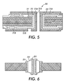
- FIG. 5 is a schematic view of a further embodiment of a via structure that is configured for electrical and fluidic interconnection.
- FIG. 6 is a schematic view of another embodiment of a via structure that is configured for electrical and fluidic interconnection.
- FIG. 1 is schematic block diagram of an embodiment of a drop-on-demand printing apparatus that includes a controller 10 and a printhead assembly 20 that can include a plurality of drop emitting drop generators.
- the printhead 20 receives ink 33 from an ink supply system 50 that can comprise at least one on-board ink reservoir and/or at least one remote ink reservoir.
- the controller 10 selectively energizes the drop generators by providing a respective drive signal to each drop generator.
- Each of the drop generators can employ a piezoelectric transducer.
- each of the drop generators can employ a shear-mode transducer, an annular constrictive transducer, an electrostrictive transducer, an electromagnetic transducer, or a magnetorestrictive transducer.
- FIG. 2 is a schematic elevational view of an embodiment of an ink jet printhead assembly 20 that can implement a plurality of drop generators 30 ( FIG. 3 ), for example as an array of drop generators.
- the ink jet printhead assembly includes a fluid channel layer or substructure 131 , a diaphragm layer 137 attached to the fluid channel layer 131 , a transducer layer 139 attached to the diaphragm layer 137 , a circuit carrying/supporting substrate 143 , and an interconnect structure 141 disposed between the circuit carrying substrate 143 and the substructure comprising the transducer layer 139 , the diaphragm layer 137 , and the fluid channel substructure 131 .
- the circuit carrying/supporting substrate 143 can comprise a printed circuit board, a flexible printed circuit, a ceramic substrate, a plastic substrate, a glass substrate, or a thin film substrate.
- the fluid channel layer 131 can implement the fluid channels and chambers of the drop generators, while the diaphragm layer 137 can implement diaphragms of the drop generators.
- the transducer layer 139 can implement the electromechanical transducers of the drop generators.
- fluid channel substructure 131 can be formed of a stack of laminated sheets or plates, such as of stainless steel.
- the circuit carrying substrate 143 feeds through the interconnect structure 141 electrical drive signals/waveforms to the transducer layer 139 as well as ink to the fluid channel layer 131 .
- the interconnect structure 141 provides fluidic and electrical interconnection between the circuit carrying substrate 143 and the transducer layer 139 and the fluid channel layer 131 .
- FIG. 3 is a schematic block diagram of an embodiment of a drop generator 30 that can be implemented in the printhead assembly 20 of the printing apparatus shown in FIG. 1 .
- the drop generator 30 includes an inlet channel 31 that receives ink 33 from the ink supply system 50 ( FIG. 1 ) through a via structure 243 formed in the circuit carrying substrate 143 and an opening 241 in a standoff 341 of the interconnect structure 141 ( FIG. 2 ).
- the ink 33 flows into an ink pressure or pump chamber 35 that is bounded on one side, for example, by a flexible diaphragm 37 that can comprise metal such as stainless steel.
- An electromechanical transducer 39 is attached to the flexible diaphragm 37 and can overlie the pressure chamber 35 , for example.
- a contact element 441 of the interconnect structure 141 electrically connects the electromechanical transducer 39 to a contact pad 343 on the circuit carrying substrate 143 .
- Electrical actuation of the electromechanical transducer 39 causes ink to flow from the pressure chamber 35 to a drop forming nozzle or orifice 47 , from which an ink drop 49 is emitted toward a receiver medium 48 that can be a transfer surface or an output medium such as paper, for example.
- the ink 33 can be melted or phase changed solid ink, and the electromechanical transducer 39 can be a piezoelectric transducer that is operated in a bending mode, for example.
- the contact element 441 can comprise silver epoxy or a conductive silicone adhesive.
- the via structure 243 is configured to conduct electrical signals, for example to the electromechanical transducer 39 , and also to convey liquid from one side of the circuit carrying substrate 143 to the other side.
- the via structure 243 can comprise a an electrically conductive layer 211 disposed in an opening in the circuit carrying substrate 143 , for example extending from a first side to second side of the circuit carrying substrate 143 , and a dielectric or electrically insulating layer 213 disposed on the electrically conductive layer 211 .
- the dielectric layer 213 functions to prevent direct liquid contact with the electrically conductive layer 211 , and is of sufficient extent to prevent liquid flowing the via structure from coming into contact with the conductive layer 211 .
- An exposed portion of the conductive layer 211 on the second side of the circuit carrying substrate 143 can comprise the contact pad 343 .
- Electrically insulating the electrically conductive layer 211 can be beneficial in applications wherein a ground plane is close to the electrically conductive layer 211 , for example wherein the diaphragm layer 137 ( FIG. 3 ) comprises a metallic ground plane. In such applications, the electrical insulation can prevent the formation of an electrochemical cell with electrical conduction and electrically-induced corrosion between an electrically active via and the ground plane.
- the dielectric layer 213 can be realized by an organic or inorganic coating or film that can be conformal.
- organic coatings examples include Parylene, polytetrafluorethylene, and polyurethane.
- Organic coatings generally can be thermally vapor deposited, although Parylene vapor deposition is performed at close to room temperature.
- a Parylene coating can be hardened or annealed using thermal or radiation means.
- inorganic coatings include anodic films that are formed from anodization of metals such as aluminum, tantalum, titanium, zinc, magnesium and niobium.
- Anodization is an electrolytic passivation process that increases the thickness of the natural oxide layer on the surface of metals, and can produce good electrical insulators that have been used as dielectric films for electrolytic capacitors.
- a sealing substance may be applied to the anodized surface to seal the porous film and improve corrosion resistance.
- anodizing aluminum using chromic, sulfuric, phosphoric or organic acid baths may produce aluminum oxide films that are porous and may require a post anodization sealing process step.
- Aluminum oxide substantially free of pores can be made using borate and tartrate baths since aluminum oxide is insoluble in these solutions.
- aluminum oxide, titanium oxide, titanium nitride and tantalum pentoxide (used in tantalum capacitors) dielectric films are possible. These metals and anodic films may generally be compatible with thin film processing.
- inorganic electrically insulating coatings include silicon dioxide, silicon oxy nitride, and silicon nitride thin films. Such films can be formed by chemical vapor deposition or sputter deposition.
- the via structure 243 can comprise a first electrically conductive layer 211 disposed in an opening in the circuit carrying substrate 143 , for example extending from a first side to second side of the circuit carrying substrate 143 , a dielectric or electrically insulating layer 213 disposed on the first electrically conductive layer 211 , and a second electrically conductive layer 215 A, 215 B disposed on the electrically insulating layer 213 .
- the second electrically conductive layer 215 A, 215 B includes a first portion 215 A that extends from the first side to the second side of the printed circuit board, and a second portion 215 B disposed on the second side of the printed circuit board and electrically isolated from the first portion 215 B of the second electrically conductive layer 215 A, 215 B.
- the second portion 215 B of the second electrically conductive layer is electrically connected to the first electrically conductive layer 211 .
- a third electrically conductive layer 217 A, 217 B can be formed on the second electrically conductive layer 215 A, 215 B in such a manner that second portions 215 B, 217 B are electrically isolated from the first portions 215 A, 217 A which are electrically connected to the first electrically conductive layer 211 .
- the portion 217 B of the third electrically conductive layer 217 A, 217 B disposed on the second portion 215 B of the second electrically conductive layer 215 A, 215 B can comprise a contact pad for electrical interconnection.
- the first and second conductive layers can comprise copper while the third conductive layer can comprise nickel. More generally, the third electrically conductive layer can comprise a material that is different from the material of the second electrically conductive layer.
- the third electrically conductive layer can be omitted, and in such implementations, an appropriate exposed portion of the second portion 215 B of the electrically conductive layer 215 A, 215 B can comprise a contact pad.
- via structure that includes a first conductive layer 211 , a drilled electrically insulating or dielectric layer 213 disposed on the first conductive layer 211 , and a second conductive layer 215 disposed on the drilled electrically insulating layer 213 .
- the second conductive layer 215 can comprise first and second electrically isolated portions as described above relative to FIG. 5 , wherein one of such portions can be electrically connected to the first electrically conductive layer.
- a third conductive layer can be optionally formed on the second conductive layer 215 as described above relative to FIG. 5 .
- the via structure can be implemented by mechanical or laser drilling a via or opening in the printed circuit board, forming the first conductive layer 211 (for example by plating), filling the plated via with an electrically insulating material such as epoxy, drilling the filled via to form the electrically insulating layer 213 , and forming the second conductive layer 215 (for example by via plating).
- the disclosed via structures can be implemented using a variety of processes including for example printed circuit board techniques, flex circuit manufacturing techniques, thick film processes, or thin film processes.
Landscapes
- Engineering & Computer Science (AREA)
- Microelectronics & Electronic Packaging (AREA)
- Particle Formation And Scattering Control In Inkjet Printers (AREA)
Abstract
Description
Claims (19)
Priority Applications (1)
| Application Number | Priority Date | Filing Date | Title |
|---|---|---|---|
| US12/338,169 US8079667B2 (en) | 2008-12-18 | 2008-12-18 | Drop generating apparatus |
Applications Claiming Priority (1)
| Application Number | Priority Date | Filing Date | Title |
|---|---|---|---|
| US12/338,169 US8079667B2 (en) | 2008-12-18 | 2008-12-18 | Drop generating apparatus |
Publications (2)
| Publication Number | Publication Date |
|---|---|
| US20100156997A1 US20100156997A1 (en) | 2010-06-24 |
| US8079667B2 true US8079667B2 (en) | 2011-12-20 |
Family
ID=42265419
Family Applications (1)
| Application Number | Title | Priority Date | Filing Date |
|---|---|---|---|
| US12/338,169 Expired - Fee Related US8079667B2 (en) | 2008-12-18 | 2008-12-18 | Drop generating apparatus |
Country Status (1)
| Country | Link |
|---|---|
| US (1) | US8079667B2 (en) |
Families Citing this family (5)
| Publication number | Priority date | Publication date | Assignee | Title |
|---|---|---|---|---|
| JP2014226790A (en) * | 2013-05-17 | 2014-12-08 | コニカミノルタ株式会社 | Inkjet head and wiring drawing-out method for inkjet head |
| JP6264654B2 (en) | 2014-03-26 | 2018-01-24 | ブラザー工業株式会社 | Liquid ejection device and method of manufacturing liquid ejection device |
| JP6213335B2 (en) * | 2014-03-26 | 2017-10-18 | ブラザー工業株式会社 | Liquid ejection device |
| JP6565238B2 (en) * | 2015-03-17 | 2019-08-28 | セイコーエプソン株式会社 | Liquid jet head |
| JP6965662B2 (en) * | 2017-09-26 | 2021-11-10 | コニカミノルタ株式会社 | Inkjet heads, methods for manufacturing inkjet heads, and image forming equipment |
Citations (8)
| Publication number | Priority date | Publication date | Assignee | Title |
|---|---|---|---|---|
| US5010355A (en) | 1989-12-26 | 1991-04-23 | Xerox Corporation | Ink jet printhead having ionic passivation of electrical circuitry |
| US6151045A (en) * | 1999-01-22 | 2000-11-21 | Lexmark International, Inc. | Surface modified nozzle plate |
| US6256053B1 (en) * | 1999-03-25 | 2001-07-03 | Fuji Photo Film Co., Ltd. | Thermal head |
| US6491384B2 (en) * | 1997-01-24 | 2002-12-10 | Seiko Epson Corporation | Ink jet printer head |
| WO2004110768A1 (en) * | 2003-06-17 | 2004-12-23 | Korea Institute Of Industrial Technology | Pieyoelectric ink jet printer head and its manufacturing process |
| US20050024396A1 (en) * | 2003-07-30 | 2005-02-03 | Isaac Farr | Printing device having a printing fluid detector |
| US7066582B2 (en) * | 2002-08-12 | 2006-06-27 | Sharp Kabushiki Kaisha | Method for producing organic insulating coating and ink-jet printhead produced according to the method |
| US7168791B2 (en) | 2000-09-15 | 2007-01-30 | Dimatix, Inc. | Piezoelectric ink jet printing module |
-
2008
- 2008-12-18 US US12/338,169 patent/US8079667B2/en not_active Expired - Fee Related
Patent Citations (8)
| Publication number | Priority date | Publication date | Assignee | Title |
|---|---|---|---|---|
| US5010355A (en) | 1989-12-26 | 1991-04-23 | Xerox Corporation | Ink jet printhead having ionic passivation of electrical circuitry |
| US6491384B2 (en) * | 1997-01-24 | 2002-12-10 | Seiko Epson Corporation | Ink jet printer head |
| US6151045A (en) * | 1999-01-22 | 2000-11-21 | Lexmark International, Inc. | Surface modified nozzle plate |
| US6256053B1 (en) * | 1999-03-25 | 2001-07-03 | Fuji Photo Film Co., Ltd. | Thermal head |
| US7168791B2 (en) | 2000-09-15 | 2007-01-30 | Dimatix, Inc. | Piezoelectric ink jet printing module |
| US7066582B2 (en) * | 2002-08-12 | 2006-06-27 | Sharp Kabushiki Kaisha | Method for producing organic insulating coating and ink-jet printhead produced according to the method |
| WO2004110768A1 (en) * | 2003-06-17 | 2004-12-23 | Korea Institute Of Industrial Technology | Pieyoelectric ink jet printer head and its manufacturing process |
| US20050024396A1 (en) * | 2003-07-30 | 2005-02-03 | Isaac Farr | Printing device having a printing fluid detector |
Non-Patent Citations (4)
| Title |
|---|
| http://www.aqmd.gov/rules/rulesreq.html-South Coast Air Quality Management District Rules and Regulations, Rule 1126, "Magnet Wire Coating Operations", Amended 1995. |
| http://www/e[a/gpv/ttn/chief/ap42/ch04-Technology Transfer Network Clearinghouse for Inventories & Emission Factors, AP42, Fifth Edition, vol. 1, Chapter 4: Evaporation Loss Sources, Section 4.2.2.3, Apr. 1981. |
| McGraw Hill, Publisher, 1970, USA, "Plastic Coatings for Electronics," by James J. Licari, pp. 1-56. |
| McGraw Hill, Publisher, 1970, USA, "Plastic Coatings for Electronics," by James J. Licari, pp. 57-84 and 106-114. |
Also Published As
| Publication number | Publication date |
|---|---|
| US20100156997A1 (en) | 2010-06-24 |
Similar Documents
| Publication | Publication Date | Title |
|---|---|---|
| US20100159193A1 (en) | Combined electrical and fluidic interconnect via structure | |
| US8079667B2 (en) | Drop generating apparatus | |
| EP0109756B1 (en) | A method of construction of a monolithic ink jet print head | |
| US7745307B2 (en) | Method of manufacturing an inkjet head through the anodic bonding of silicon members | |
| JP5837978B2 (en) | Liquid discharge head and recording apparatus using the same | |
| US8556383B2 (en) | Liquid ejecting head and liquid ejecting apparatus | |
| US8397359B2 (en) | Method of manufacturing a drop generator | |
| JP2009107348A (en) | Method for manufacturing ink-jet printhead | |
| JP2012086426A (en) | Liquid ejecting head unit | |
| KR20110096797A (en) | Inkjet Printhead and Inkjet Printhead Manufacturing Method | |
| JP2009226923A (en) | Liquid jet head, liquid jet apparatus, and actuator device | |
| JP4878111B2 (en) | Cell driving type piezoelectric / electrostrictive actuator and manufacturing method thereof | |
| US6955419B2 (en) | Ink jet apparatus | |
| EP1498268A1 (en) | Liquid delivering apparatus and method of producing the same | |
| US7048361B2 (en) | Ink jet apparatus | |
| JP2010214795A (en) | Liquid droplet jetting apparatus, and manufacturing method for liquid droplet jetting apparatus | |
| JP2007268838A (en) | Inkjet head | |
| US9517624B2 (en) | Wiring mounting structure and method of manufacturing the same, and liquid ejecting head and liquid ejecting apparatus | |
| JP2000218792A (en) | Inkjet head | |
| JP2004106380A (en) | Piezoelectric base for shearing mode type inkjet head, and method for forming electrode of piezoelectric base for shearing mode type inkjet head | |
| JP2771008B2 (en) | Recording device and recording head | |
| JP2007275711A (en) | Surface modification method, method for manufacturing substrate with film, droplet ejection head, and droplet ejection apparatus | |
| CN1504334A (en) | Porous back-shooting type ink-jet printing module and manufacturing method thereof | |
| JP2007062034A (en) | Wiring structure, device, device manufacturing method, droplet discharge head, droplet discharge head manufacturing method, and droplet discharge apparatus | |
| JP2019001009A (en) | Inkjet head, inkjet head manufacturing method, and inkjet recording apparatus |
Legal Events
| Date | Code | Title | Description |
|---|---|---|---|
| AS | Assignment |
Owner name: XEROX CORPORATION,CONNECTICUT Free format text: ASSIGNMENT OF ASSIGNORS INTEREST;ASSIGNORS:ANDREWS, JOHN R.;GERVASI, DAVID J.;REEL/FRAME:022274/0984 Effective date: 20090211 Owner name: PALO ALTO RESEARCH CENTER INCORPORATED,CALIFORNIA Free format text: ASSIGNMENT OF ASSIGNORS INTEREST;ASSIGNORS:YOUNG, MICHAEL Y.;CHEUNG, PATRICK C.;WHITE, STEPHEN DAVID;SIGNING DATES FROM 20090211 TO 20090212;REEL/FRAME:022275/0160 Owner name: XEROX CORPORATION, CONNECTICUT Free format text: ASSIGNMENT OF ASSIGNORS INTEREST;ASSIGNORS:ANDREWS, JOHN R.;GERVASI, DAVID J.;REEL/FRAME:022274/0984 Effective date: 20090211 Owner name: PALO ALTO RESEARCH CENTER INCORPORATED, CALIFORNIA Free format text: ASSIGNMENT OF ASSIGNORS INTEREST;ASSIGNORS:YOUNG, MICHAEL Y.;CHEUNG, PATRICK C.;WHITE, STEPHEN DAVID;SIGNING DATES FROM 20090211 TO 20090212;REEL/FRAME:022275/0160 |
|
| STCF | Information on status: patent grant |
Free format text: PATENTED CASE |
|
| FPAY | Fee payment |
Year of fee payment: 4 |
|
| FEPP | Fee payment procedure |
Free format text: MAINTENANCE FEE REMINDER MAILED (ORIGINAL EVENT CODE: REM.); ENTITY STATUS OF PATENT OWNER: LARGE ENTITY |
|
| LAPS | Lapse for failure to pay maintenance fees |
Free format text: PATENT EXPIRED FOR FAILURE TO PAY MAINTENANCE FEES (ORIGINAL EVENT CODE: EXP.); ENTITY STATUS OF PATENT OWNER: LARGE ENTITY |
|
| STCH | Information on status: patent discontinuation |
Free format text: PATENT EXPIRED DUE TO NONPAYMENT OF MAINTENANCE FEES UNDER 37 CFR 1.362 |
|
| FP | Lapsed due to failure to pay maintenance fee |
Effective date: 20191220 |