US8076969B1 - Apparatus for attenuating low frequency signals - Google Patents

Apparatus for attenuating low frequency signals Download PDF

Info

Publication number
US8076969B1
US8076969B1 US12/413,654 US41365409A US8076969B1 US 8076969 B1 US8076969 B1 US 8076969B1 US 41365409 A US41365409 A US 41365409A US 8076969 B1 US8076969 B1 US 8076969B1
Authority
US
United States
Prior art keywords
region
pass filter
high pass
source
node
Prior art date
Legal status (The legal status is an assumption and is not a legal conclusion. Google has not performed a legal analysis and makes no representation as to the accuracy of the status listed.)
Expired - Fee Related
Application number
US12/413,654
Inventor
Thart Fah Voo
Current Assignee (The listed assignees may be inaccurate. Google has not performed a legal analysis and makes no representation or warranty as to the accuracy of the list.)
Cavium International
Marvell Asia Pte Ltd
Original Assignee
Marvell International Ltd
Priority date (The priority date is an assumption and is not a legal conclusion. Google has not performed a legal analysis and makes no representation as to the accuracy of the date listed.)
Filing date
Publication date
Application filed by Marvell International Ltd filed Critical Marvell International Ltd
Priority to US12/413,654 priority Critical patent/US8076969B1/en
Application granted granted Critical
Publication of US8076969B1 publication Critical patent/US8076969B1/en
Assigned to CAVIUM INTERNATIONAL reassignment CAVIUM INTERNATIONAL ASSIGNMENT OF ASSIGNORS INTEREST (SEE DOCUMENT FOR DETAILS). Assignors: MARVELL INTERNATIONAL LTD.
Assigned to MARVELL ASIA PTE, LTD. reassignment MARVELL ASIA PTE, LTD. ASSIGNMENT OF ASSIGNORS INTEREST (SEE DOCUMENT FOR DETAILS). Assignors: CAVIUM INTERNATIONAL
Expired - Fee Related legal-status Critical Current
Anticipated expiration legal-status Critical

Links

Images

Classifications

    • HELECTRICITY
    • H03ELECTRONIC CIRCUITRY
    • H03KPULSE TECHNIQUE
    • H03K5/00Manipulating of pulses not covered by one of the other main groups of this subclass
    • H03K5/003Changing the DC level
    • HELECTRICITY
    • H03ELECTRONIC CIRCUITRY
    • H03FAMPLIFIERS
    • H03F1/00Details of amplifiers with only discharge tubes, only semiconductor devices or only unspecified devices as amplifying elements
    • H03F1/56Modifications of input or output impedances, not otherwise provided for
    • HELECTRICITY
    • H03ELECTRONIC CIRCUITRY
    • H03HIMPEDANCE NETWORKS, e.g. RESONANT CIRCUITS; RESONATORS
    • H03H1/00Constructional details of impedance networks whose electrical mode of operation is not specified or applicable to more than one type of network
    • H03H1/02Constructional details of impedance networks whose electrical mode of operation is not specified or applicable to more than one type of network of RC networks, e.g. integrated networks
    • HELECTRICITY
    • H03ELECTRONIC CIRCUITRY
    • H03FAMPLIFIERS
    • H03F2200/00Indexing scheme relating to amplifiers
    • H03F2200/27A biasing circuit node being switched in an amplifier circuit
    • HELECTRICITY
    • H03ELECTRONIC CIRCUITRY
    • H03FAMPLIFIERS
    • H03F2200/00Indexing scheme relating to amplifiers
    • H03F2200/54Two or more capacitor coupled amplifier stages in cascade
    • HELECTRICITY
    • H03ELECTRONIC CIRCUITRY
    • H03HIMPEDANCE NETWORKS, e.g. RESONANT CIRCUITS; RESONATORS
    • H03H7/00Multiple-port networks comprising only passive electrical elements as network components
    • H03H7/01Frequency selective two-port networks
    • H03H7/12Bandpass or bandstop filters with adjustable bandwidth and fixed centre frequency

Definitions

  • the present invention relates generally to high pass filters.
  • High pass filters pass high frequency signals above a cutoff frequency and attenuate low frequency signals below the cutoff frequency. High pass filters typically cannot achieve very low cutoff frequencies due to diode leakage current.
  • a capacitor C HP is connected to an output of Amp 1 , and an input of Amp 2 .
  • Resistors R 1 , R 2 , . . . , and R n are connected in parallel to one end of the capacitor C HP and the input of Amp 2 , and to a source node of transistors M 1 , M 2 , . . . , and M n and a cathode of diodes D 11 , D 21 , . . . , and D n1 .
  • a source node of transistor M CH is connected to one end of the capacitor C HP and the input of Amp 2 , and to a cathode of diode D o1 .
  • a drain node of transistors M 1 , M 2 , . . . , M n , and M CH is connected to a cathode of diodes D 12 , D 22 , . . . , D n2 , and D o2 and to the reference node V REF .
  • the anodes of diodes D 11 , D 21 , . . . , D n1 , D 12 , D 22 , . . . , D n2 , D o1 , and D o2 are connected to ground.
  • the transistors M 1 , M 2 , . . . , M n , and M CH receive control signals MSW 1 , MSW 2 , . . . , MSW n , and CLK, respectively, which control transistors M 1 , M 2 , . . . , M n , and M CH .
  • Transistors M 1 , M 2 , . . . , and M n open or close bias networks 20 of different resistances based on a desired cutoff frequency of the high-pass filter.
  • the cutoff frequency represents the frequency at which the output power is half the input power.
  • the transistor M CH is controlled by the clock signal CLK and is used to charge the capacitor C HP using voltage V REF during initialization.
  • the resistance through paths R 1 , R 2 , . . . , and R n may be too large, thereby increasing a time to charge capacitor C HP .
  • the bias network 20 includes an NMOS transistor M 1 fabricated using a twin-well process.
  • a resistor R 1 is connected at one end to a communication node V C , and at the other end to a source of the transistor M 1 and a cathode of a diode D 11 .
  • the drain of transistor M 1 is connected to a cathode of diode D 12 and a reference node V REF1 .
  • Control signal MSW 1 controls the switching of transistor M 1 .
  • Anodes of diodes D 1 , D 12 are connected to an anode of diode D 13 .
  • a cathode of diode D 13 is connected to a second reference node V REF2 and to a cathode of diode D 14 .
  • An anode of diode D 14 is connected to ground.
  • a deep n-well 34 is formed in a p-type substrate 32 .
  • a p-well 36 is formed in the deep n-well 34 .
  • An n+ source region 38 and an n+ drain region 40 are formed in the p-well 36 .
  • Diodes D 11 -D 14 are inherent in regions between n-type and p-type regions (i.e. p-n junctions). For example, current flows from the p-type side (the anode) to the n-type side (the cathode).
  • a diode D 11 is inherently present in the region 42 between the source 38 and the p-well 36 .
  • a diode D 12 is inherently present in the region 44 between the drain 40 and the p-well 36 .
  • a diode D 13 is inherently present in the region 46 between the p-well 36 and the deep n-well 34 .
  • a diode D 14 is inherently present in the region 48 between the deep n-well 34 and the p-type substrate 32 .
  • a variable frequency module controls a cutoff frequency of a high pass filter and includes a resistive element that communicates with a capacitive element of the high pass filter.
  • a first transistor communicates with the resistive element and a reference node and includes a first source/drain region formed in a first well region and a first diode region formed between the first source/drain region and the first well region.
  • a first node of the first diode region is connected to the first source/drain region and the reference node, and a second node of the first diode region is connected to the reference node.
  • the first transistor further includes a first contact region formed in the first well region that is connected to the first source/drain region and the first well region.
  • the first transistor further includes a second diode region formed between a second source/drain region and the first well region. A first node of the second diode region is connected to the second source/drain region, and a second node of the second diode region is connected to the second node of the first diode region and the reference node.
  • a second transistor communicates with the capacitive element and the reference node and includes a third source/drain region formed in a second well region and a third diode region formed between the third source/drain region and the second well region.
  • a first node of the third diode region is connected to the third source/drain region and the reference node, and a second node of the third diode region is connected to the reference node.
  • the second transistor further includes a second contact region formed in the second well region that is connected to the third source/drain region and the second well region.
  • the second transistor further includes a fourth diode formed between a fourth source/drain region and the second well region.
  • a first node of the fourth diode region is connected to the fourth source/drain region, and a second node of the fourth diode region is connected to the second node of the third diode region and the reference node.
  • the first transistor and the second transistor are of a twin-well design.
  • variable frequency module receives a reference voltage signal.
  • the reference node receives the reference voltage signal.
  • variable frequency module includes an input signal and an output signal.
  • a first node of the capacitive element receives the input signal, a second node of the capacitive element communicates with a communication node of the variable frequency module, and the output signal is generated at the second node of the capacitive element.
  • the first transistor receives a program signal.
  • the second transistor receives a clock signal.
  • a variable frequency module that controls a cutoff frequency of a high pass filter includes a resistive element that communicates with a capacitive element of the high pass filter.
  • a transistor includes a source/drain region formed in a well region, a diode region formed between the source/drain region and the well region, and a contact region formed in the well region. The contact region is connected to the source/drain region, the well region, and a reference voltage.
  • the resistive element includes N resistors and further the variable frequency module further includes N ⁇ 1 of the transistors. First ends of each of the N resistors are connected together. Second ends of each of the N resistors communicate with a respective one of the N transistors. N is an integer greater than or equal to 2.
  • variable frequency module further includes N additional resistive elements and N additional transistors that each include a source/drain region formed in a well region, a diode region formed between the source/drain region and the well region, and a contact region formed in the well region.
  • a first end of each of the N additional resistive elements connects to an associated one of the N additional transistors and a second end of each of the N additional resistive elements connects to an adjacent one of the N+1 transistors and wherein N is an integer greater than or equal to 1.
  • the transistors are NMOS transistors and/or PMOS transistors.
  • a variable frequency module that controls a cutoff frequency of a high pass filter includes resistive means for communicating with a capacitive means for providing a capacitance of the high pass filter.
  • First transistor means communicate with the resistive means and a reference node and include a first source/drain region formed in a first well region and a first diode region formed between the first source/drain region and the first well region. A first node of the first diode region is connected to the first source/drain region and the reference node, and a second node of the first diode region is connected to the reference node.
  • the first transistor means further includes a first contact region formed in the first well region that is connected to the first source/drain region and the first well region.
  • the first transistor means further includes a second diode region formed between a second source/drain region and the first well region. A first node of the second diode region is connected to the second source/drain region, and a second node of the second diode region is connected to the second node of the first diode region and the reference node.
  • variable frequency module further includes second transistor means for communicating with the capacitive means and the reference node and includes a third source/drain region formed in a second well region and a third diode region formed between the third source/drain region and the second well region.
  • a first node of the third diode region is connected to the third source/drain region and the reference node, and a second node of the third diode region is connected to the reference node.
  • the second transistor means further includes a second contact region formed in the second well region that is connected to the third source/drain region and the second well region.
  • the second transistor means further includes a fourth diode formed between a fourth source/drain region and the second well region.
  • a first node of the fourth diode region is connected to the fourth source/drain region, and a second node of the fourth diode region is connected to the second node of the third diode region and the reference node.
  • the first transistor means and the second transistor means are of a twin-well design.
  • variable frequency module receives a reference voltage signal.
  • the reference node receives the reference voltage signal.
  • the variable frequency module also includes an input signal and an output signal.
  • a first node of the capacitive means receives the input signal, a second node of the capacitive means communicates with a communication node of the variable frequency module, and the output signal is generated at the second node of the capacitive means.
  • the first transistor means receives a program signal.
  • the second transistor means receives a clock signal.
  • a variable frequency module controls a cutoff frequency of a high pass filter and includes resistive means for communicating with capacitive means for providing a capacitance of the high pass filter.
  • Transistor means for communicating with the resistive means include a source/drain region formed in a well region, a diode region formed between the source/drain region and the well region, and a contact region formed in the well region. The contact region is connected to the source/drain region, the well region, and a reference voltage.
  • the resistive means includes N resistor means for providing resistances and the variable frequency module further includes N ⁇ 1 transistor means for communicating with respective ones of the N resistor means. Each of the N resistor means are connected together. Second ends of each of the N resistor means communicates with a respective one of the N transistor means. N is an integer greater than or equal to 2.
  • variable frequency module further includes N additional resistive means for providing resistances and N additional transistor means for controlling current that flows through the N additional resistive means.
  • Each of the N additional transistor means includes a source/drain region formed in a well region, a diode region formed between the source/drain region and the well region, and a contact region formed in the well region.
  • a first end of each of the N additional resistive means connects to an associated one of the N additional transistor means and a second end of each of the N additional resistive means connects to an adjacent one of the N+1 transistor means.
  • N is an integer greater than or equal to 1.
  • Each of the N+1 transistor means implements an NMOS and/or PMOS transistor.
  • FIG. 1 is a circuit diagram of a high pass filter
  • FIG. 2 is a circuit diagram of a bias network of the high pass filter of FIG. 1 using an NMOS transistor fabricated using a twin-well process;
  • FIG. 3 is a cross-sectional diagram of an NMOS transistor fabricated using a twin-well process
  • FIG. 4 is a circuit diagram of a high pass filter with a variable frequency control module
  • FIG. 5 is a circuit diagram of the variable frequency control module
  • FIG. 6 is a circuit diagram of the variable frequency control module
  • FIG. 7A is a circuit diagram of the diode connections required to implement the variable frequency module using NMOS technology
  • FIG. 7B is a circuit diagram representing the equivalent circuit after the connecting of the diodes of the variable frequency module using NMOS technology
  • FIG. 7D is a circuit diagram representing the equivalent circuit after the connecting of the diodes of the variable frequency module using PMOS technology
  • FIG. 8 is a cross-sectional diagram of an NMOS transistor fabricated using a twin-well process with a diode bypass connection
  • FIG. 9 is a cross-sectional diagram of a PMOS transistor fabricated using a twin-well process with a diode bypass connection
  • FIG. 10 is a circuit diagram representing the equivalent circuit after the connecting of the diodes of the variable frequency module using PMOS technology of FIG. 9 ;
  • FIG. 11A is a functional block diagram of a hard disk drive
  • FIG. 11B is a functional block diagram of a digital versatile disk (DVD).
  • DVD digital versatile disk
  • FIG. 11C is a functional block diagram of a high definition television
  • FIG. 11D is a functional block diagram of a vehicle control system
  • FIG. 11E is a functional block diagram of a cellular phone
  • FIG. 11F is a functional block diagram of a set top box.
  • FIG. 11G is a functional block diagram of a media player.
  • module, circuit and/or device refers to an Application Specific Integrated Circuit (ASIC), an electronic circuit, a processor (shared, dedicated, or group) and memory that execute one or more software or firmware programs, a combinational logic circuit, and/or other suitable components that provide the described function.
  • ASIC Application Specific Integrated Circuit
  • processor shared, dedicated, or group
  • memory that execute one or more software or firmware programs, a combinational logic circuit, and/or other suitable components that provide the described function.
  • phrase at least one of A, B, and C should be construed to mean a logical (A or B or C), using a non-exclusive logical or. It should be understood that steps within a method may be executed in different order without altering the principles of the present disclosure.
  • a high-pass filter 50 with amplifiers Amp 1 , Amp 2 , and a variable frequency module 52 is shown.
  • a capacitor C HP is connected to an output of Amp 1 and an input of Amp 2 .
  • the variable frequency module 52 receives a reference voltage signal V REF , and controls a resistive path of the high-pass filter 50 .
  • the variable frequency module 52 allows the high pass filter 50 to achieve a low cutoff frequency based on the connections of the inherent diodes. Normally, diodes D 11 , D 21 , . . . , D n1 , D 12 , D 22 , . .
  • variable frequency module 52 connects the anode of diodes D 11 , D 21 , . . . , D n1 , and D o1 to V REF , effectively bypassing diodes D 21 , D 22 , D n2 , and D o2 .
  • This connection prevents leakage current from draining capacitor C HP , and helps hold V C by forward biasing diodes D 11 , D 21 , . . . , D n1 , and D o1 using V REF . Therefore, by preventing this leakage current and holding V C , the variable frequency module 52 creates a lower cutoff frequency for the high pass filter 50 .
  • a communication node V C is connected to the first ends of resistors R 1 , R 2 , . . . , and R n , the cathode of diode D o1 , and the source of transistor M CH .
  • resistors R 1 , R 2 , . . . , and R n those skilled in the art can appreciate that other resistive elements may be used.
  • the second ends of resistors R 1 -R n are connected to the sources of transistors M 1 , M 2 , . . . , and M n and the cathodes of diodes D 11 , D 21 , .
  • the drains of transistors M 1 , M 2 , . . . , M n , and M CH are connected to the anodes of diodes D 11 , D 21 , . . . , D n1 , D 21 , D 22 , . . . , D n2 , D o1 , and D o2 and to V REF .
  • These connections effectively bypass diodes D 21 , D 22 , . . . , D n2 , and D o2 , preventing leakage current from draining V C and holding V C by forward biasing diodes D 11 , D 21 , . . . , D n1 , and D o1 .
  • Control signals MSW 1 , MSW 2 , . . . , and MSW n control the various NMOS bias transistors M 1 , M 2 , . . . , and M n , which open paths of different resistances based on the desired cutoff frequency of the high-pass filter.
  • a control module (not shown) may send a control signal that opens a path of higher resistance, which creates a lower cutoff frequency.
  • the transistor M CH controlled by the clock signal CLK, is used to charge the capacitor C HP using voltage V REF during initialization.
  • the resistance through paths R 1 , R 2 , . . . , and R n may be too large, thereby increasing a time to charge capacitor C HP .
  • the communication voltage signal V C is high impedance.
  • the diodes D 21 , . . . , and D n1 , D 12 , D 22 , . . . , and D n2 , D o1 , and D o2 are connected as shown in FIG. 1 , node V C will drain off due to diode leakage current, which creates a higher cutoff frequency than is desired.
  • the diodes do not drain current from node V.
  • V REF forward biases the first diodes D 11 , D 21 , . . . , D n1 , and D o1 .
  • the first diodes D 11 , D 21 , . . . , D n1 , and D o1 help to maintain the voltage at node V C by supplying current.
  • FIG. 6 a circuit diagram of the variable frequency module 52 is shown with resistors R 1 , R 2 , . . . , and R n connected in a series pattern as opposed to the parallel pattern of FIG. 5 .
  • Communication node V C is connected to the first end of resistor R 1 and the cathode of diode D o1 , and the source of transistor M CH .
  • the first end of resistor R 2 is connected to the second end of resistor R 1 .
  • the first end of resistor R n is connected to the second end of resistor R n-1 and the second end of resistor R n is connected to the cathode of diode D n1 and the source of transistor M n .
  • the remaining elements and their associated connections, and the control signals MSW 1 -MSW n are the same as shown in FIG. 5 .
  • FIGS. 7A-7B diode connections for NMOS transistors are shown.
  • the connection of the diode D NMOS1 bypasses diode D NMOS2 .
  • the equivalent connection is shown after bypassing diode D NMOS2 (see FIG. 7A ).
  • Diode D NMOS1 can now be forward biased to help maintain the voltage at capacitor C HP (see FIG. 4 ) by providing leakage current.
  • diode connections for PMOS transistors are shown.
  • the connection of the diode D PMOS1 bypasses diode D PMOS2 .
  • the equivalent connection is shown after bypassing diode D PMOS2 (see FIG. 7C ).
  • Diode D PMOS1 can now be reverse biased to help maintain the voltage at capacitor C HP (see FIG. 4 ) by providing reverse leakage current. This PMOS configuration can be used if the twin-well process is not available.
  • FIG. 8 a cross-sectional view of an NMOS transistor 54 created using a twin-well process with a diode bypass connection is shown.
  • a deep n-well 58 is formed in a p-type substrate 56 .
  • a p-well 60 is formed in the deep n-well 58 .
  • An n+ source region 62 and an n+ drain region 64 are formed in the p-well 60 .
  • a p+ bulk contact 66 is formed in the p-well 60 near the drain region 64 .
  • Diodes D 11 -D 14 are inherent in regions between n-type and p-type regions (i.e. p-n junctions).
  • a diode D 11 is inherently present in the region 68 between the source 62 and the p-well 60 .
  • a diode D 12 is inherently present in the region 70 between the drain 64 and the p-well 60 .
  • a diode D 13 is inherently present in the region 72 between the p-well 60 and the deep n-well 58 .
  • a diode D 14 is inherently present in the region 74 between the deep n-well 58 and the p-type substrate 56 .
  • the p+ bulk contact 66 is connected to the entire p-well 60 .
  • the p+ bulk contact 66 By connecting to the entire p-well 60 , current can flow through the less resistive p+ bulk contact to p-well 60 path, as opposed to flowing through the more resistive n+ drain region 64 to p-well 60 path (diode D 12 ). Therefore, by electrically coupling the drain 64 and the p+ bulk contact 66 and connecting to V REF 76 , diode D 12 is effectively bypassed, because the drain 64 is connected to the p-well bulk contact 66 , which is connected to the anodes (the p-well bulk) of diodes D 11 , D 12 , and D 13 .
  • FIG. 9 a cross-sectional view of a PMOS transistor 84 created using the twin-well process with a diode bypass connection is shown.
  • An n-well 90 is formed in a p-type substrate 88 .
  • a p+ source region 92 and a p+ drain region 94 are formed in the n-well 90 .
  • An n+ bulk contact 96 is formed in the n-well 90 near the drain region 94 .
  • An n+ bulk contact 98 is formed in the n-well near the source region 92 .
  • a diode D 31 is inherently present in the region 98 between the source region 92 and the n-well 90 .
  • a diode D 32 is inherently present in the region 100 between the drain region 94 and the n-well 90 .
  • a diode D 33 is inherently present in a region 102 between the n-well 90 and the p-substrate 88 .
  • An anode of a diode D PMOS1 connects to a source of an ideal transistor.
  • An anode of a diode D PMOS2 connects to a drain of the ideal transistor.
  • Cathodes of diodes D PMOS1 and D PMOS2 are connected to a cathode of a diode D PMOS3 .
  • An anode of diode D PMOS3 connects to a reference voltage such as ground.
  • Signal MSW PMOS communicates with a gate of the ideal transistor.
  • variable frequency module can be implemented in high pass filters of a hard disk drive 400 .
  • the variable frequency module may be implemented in either or both signal processing and/or control circuits, which are generally identified in FIG. 5A at 402 .
  • the signal processing and/or control circuit 402 and/or other circuits (not shown) in the HDD 400 may process data, perform coding and/or encryption, perform calculations, and/or format data that is output to and/or received from a magnetic storage medium 406 .
  • the HDD 400 may communicate with a host device (not shown) such as a computer, mobile computing devices such as personal digital assistants, cellular phones, media or MP3 players and the like, and/or other devices via one or more wired or wireless communication links 408 .
  • the HDD 400 may be connected to memory 409 such as random access memory (RAM), low latency nonvolatile memory such as flash memory, read only memory (ROM) and/or other suitable electronic data storage.
  • RAM random access memory
  • ROM read only memory
  • variable frequency module can be implemented in a digital versatile disc (DVD) drive 410 .
  • the variable frequency module may be implemented in high pass filters of signal processing and/or control circuits, which are generally identified in FIG. 11B at 412 .
  • the signal processing and/or control circuit 412 and/or other circuits (not shown) in the DVD 410 may process data, perform coding and/or encryption, perform calculations, and/or format data that is read from and/or data written to an optical storage medium 416 .
  • the signal processing and/or control circuit 412 and/or other circuits (not shown) in the DVD 410 can also perform other functions such as encoding and/or decoding and/or any other signal processing functions associated with a DVD drive.
  • the DVD drive 410 may communicate with an output device (not shown) such as a computer, television or other device via one or more wired or wireless communication links 417 .
  • the DVD 410 may communicate with mass data storage 418 that stores data in a nonvolatile manner.
  • the mass data storage 418 may include a hard disk drive (HDD).
  • the HDD may have the configuration shown in FIG. 11A .
  • the HDD may be a mini HDD that includes one or more platters having a diameter that is smaller than approximately 1.8′′.
  • the DVD 410 may be connected to memory 419 such as RAM, ROM, low latency nonvolatile memory such as flash memory and/or other suitable electronic data storage.
  • variable frequency module can be implemented in high pass filters of a high definition television (HDTV) 420 .
  • the device may be implemented in either or both signal processing and/or control circuits, which are generally identified in FIG. 11E at 422 .
  • the HDTV 420 receives HDTV input signals in either a wired or wireless format and generates HDTV output signals for a display 426 .
  • signal processing circuit and/or control circuit 422 and/or other circuits (not shown) of the HDTV 420 may process data, perform coding and/or encryption, perform calculations, format data and/or perform any other type of HDTV processing that may be required.
  • the HDTV 420 may communicate with mass data storage 427 that stores data in a nonvolatile manner such as optical and/or magnetic storage devices. At least one HDD may have the configuration shown in FIG. 11A and/or at least one DVD may have the configuration shown in FIG. 11B .
  • the HDD may be a mini HDD that includes one or more platters having a diameter that is smaller than approximately 1.8′′.
  • the HDTV 420 may be connected to memory 428 such as RAM, ROM, low latency nonvolatile memory such as flash memory and/or other suitable electronic data storage.
  • the HDTV 420 also may support connections with a WLAN via a WLAN network interface 429 .
  • variable frequency module may implement and/or be implemented in high pass filters of a control system of a vehicle 430 .
  • the variable frequency module may be implemented in a powertrain control system 432 that receives inputs from one or more sensors such as temperature sensors, pressure sensors, rotational sensors, airflow sensors and/or any other suitable sensors and/or that generates one or more output control signals such as engine operating parameters, transmission operating parameters, and/or other control signals.
  • the variable frequency module may also be implemented in other control systems 440 of the vehicle 430 .
  • the control system 440 may likewise receive signals from input sensors 442 and/or output control signals to one or more output devices 444 .
  • the control system 440 may be part of an anti-lock braking system (ABS), a navigation system, a telematics system, a vehicle telematics system, a lane departure system, an adaptive cruise control system, a vehicle entertainment system such as a stereo, DVD, compact disc and the like. Still other implementations are contemplated.
  • the powertrain control system 432 may communicate with mass data storage 446 that stores data in a nonvolatile manner.
  • the mass data storage 446 may include optical and/or magnetic storage devices for example hard disk drives HDD and/or DVDs. At least one HDD may have the configuration shown in FIG. 11A and/or at least one DVD may have the configuration shown in FIG. 11B .
  • the HDD may be a mini HDD that includes one or more platters having a diameter that is smaller than approximately 1.8′′.
  • the powertrain control system 432 may be connected to memory 447 such as RAM, ROM, low latency nonvolatile memory such as flash memory and/or other suitable electronic data storage.
  • the powertrain control system 432 also may support connections with a WLAN via a WLAN network interface 448 .
  • the control system 440 may also include mass data storage, memory and/or a WLAN interface (all not shown).
  • variable frequency module can be implemented in high pass filters of a cellular phone 450 that may include a cellular antenna 451 .
  • the variable frequency module may implement and/or be implemented in either or both signal processing and/or control circuits, which are generally identified in FIG. 11E at 452 .
  • the cellular phone 450 includes a microphone 456 , an audio output 458 such as a speaker and/or audio output jack, a display 460 and/or an input device 462 such as a keypad, pointing device, voice actuation and/or other input device.
  • the signal processing and/or control circuits 452 and/or other circuits (not shown) in the cellular phone 450 may process data, perform coding and/or encryption, perform calculations, format data and/or perform other cellular phone functions.
  • the cellular phone 450 may communicate with mass data storage 464 that stores data in a nonvolatile manner such as optical and/or magnetic storage devices for example hard disk drives HDD and/or DVDs. At least one HDD may have the configuration shown in FIG. 11A and/or at least one DVD may have the configuration shown in FIG. 11B .
  • the HDD may be a mini HDD that includes one or more platters having a diameter that is smaller than approximately 1.8′′.
  • the cellular phone 450 may be connected to memory 466 such as RAM, ROM, low latency nonvolatile memory such as flash memory and/or other suitable electronic data storage.
  • the cellular phone 450 also may support connections with a WLAN via a WLAN network interface 468 .
  • variable frequency module can be implemented in high pass filters of a set top box 480 .
  • the variable frequency module may implement and/or be implemented in either or both signal processing and/or control circuits, which are generally identified in FIG. 5E at 484 .
  • the set top box 480 receives signals from a source such as a broadband source and outputs standard and/or high definition audio/video signals suitable for a display 488 such as a television and/or monitor and/or other video and/or audio output devices.
  • the signal processing and/or control circuits 484 and/or other circuits (not shown) of the set top box 480 may process data, perform coding and/or encryption, perform calculations, format data and/or perform any other set top box function.
  • the set top box 480 may communicate with mass data storage 490 that stores data in a nonvolatile manner.
  • the mass data storage 490 may include optical and/or magnetic storage devices for example hard disk drives HDD and/or DVDs. At least one HDD may have the configuration shown in FIG. 11A and/or at least one DVD may have the configuration shown in FIG. 11B .
  • the HDD may be a mini HDD that includes one or more platters having a diameter that is smaller than approximately 1.8′′.
  • the set top box 480 may be connected to memory 494 such as RAM, ROM, low latency nonvolatile memory such as flash memory and/or other suitable electronic data storage.
  • the set top box 480 also may support connections with a WLAN via a WLAN network interface 496 .
  • variable frequency module can be implemented in high pass filters of a media player 500 .
  • the variable frequency module may implement and/or be implemented in either or both signal processing and/or control circuits, which are generally identified in FIG. 11G at 504 .
  • the media player 500 includes a display 507 and/or a user input 508 such as a keypad, touchpad and the like.
  • the media player 500 may employ a graphical user interface (GUI) that typically employs menus, drop down menus, icons and/or a point-and-click interface via the display 507 and/or user input 508 .
  • the media player 500 further includes an audio output 509 such as a speaker and/or audio output jack.
  • the signal processing and/or control circuits 504 and/or other circuits (not shown) of the media player 500 may process data, perform coding and/or encryption, perform calculations, format data and/or perform any other media player function.
  • the media player 500 may communicate with mass data storage 510 that stores data such as compressed audio and/or video content in a nonvolatile manner.
  • the compressed audio files include files that are compliant with MP3 format or other suitable compressed audio and/or video formats.
  • the mass data storage may include optical and/or magnetic storage devices for example hard disk drives HDD and/or DVDs. At least one HDD may have the configuration shown in FIG. 11A and/or at least one DVD may have the configuration shown in FIG. 11B .
  • the HDD may be a mini HDD that includes one or more platters having a diameter that is smaller than approximately 1.8′′.
  • the media player 500 may be connected to memory 514 such as RAM, ROM, low latency nonvolatile memory such as flash memory and/or other suitable electronic data storage.
  • the media player 500 also may support connections with a WLAN via a WLAN network interface 516 . Still other implementations in addition to those described above are contemplated.

Abstract

A high pass filter has a cutoff frequency. The high pass filter includes a first amplifier to receive an input signal. The high pass filter attenuates low frequency signals of the input signal that are below the cutoff frequency. A second amplifier provides an output signal. The output signal comprising only high frequency signals of the input signal that are above the cutoff frequency. A capacitive element is coupled in between the first amplifier and the second amplifier. A variable frequency module controls a plurality of resistive paths of the high pass filter. Each resistive path corresponds to a different cutoff frequency for the high pass filter. The variable frequency module is configured to prevent any leakage current from draining the capacitive element.

Description

CROSS-REFERENCE TO RELATED APPLICATIONS
This application is a continuation of U.S. patent application Ser. No. 11/582,906, filed Oct. 18, 2006, which claims the benefit of U.S. Provisional Application No. 60/793,863, filed Apr. 21, 2006. The disclosures of the above applications are incorporated herein by reference.
FIELD
The present invention relates generally to high pass filters.
BACKGROUND
High pass filters pass high frequency signals above a cutoff frequency and attenuate low frequency signals below the cutoff frequency. High pass filters typically cannot achieve very low cutoff frequencies due to diode leakage current.
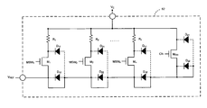
Referring now to FIG. 1, a high-pass filter 10 with amplifiers Amp1, Amp2 is shown. A capacitor CHP is connected to an output of Amp1, and an input of Amp2. Resistors R1, R2, . . . , and Rn are connected in parallel to one end of the capacitor CHP and the input of Amp2, and to a source node of transistors M1, M2, . . . , and Mn and a cathode of diodes D11, D21, . . . , and Dn1. A source node of transistor MCH is connected to one end of the capacitor CHP and the input of Amp2, and to a cathode of diode Do1. A drain node of transistors M1, M2, . . . , Mn, and MCH is connected to a cathode of diodes D12, D22, . . . , Dn2, and Do2 and to the reference node VREF. The anodes of diodes D11, D21, . . . , Dn1, D12, D22, . . . , Dn2, Do1, and Do2 are connected to ground.
The transistors M1, M2, . . . , Mn, and MCH receive control signals MSW1, MSW2, . . . , MSWn, and CLK, respectively, which control transistors M1, M2, . . . , Mn, and MCH. Transistors M1, M2, . . . , and Mn open or close bias networks 20 of different resistances based on a desired cutoff frequency of the high-pass filter. A time constant, τ=RCHP, is inversely proportional to a cutoff frequency. The cutoff frequency represents the frequency at which the output power is half the input power. The transistor MCH is controlled by the clock signal CLK and is used to charge the capacitor CHP using voltage VREF during initialization. For example, the resistance through paths R1, R2, . . . , and Rn may be too large, thereby increasing a time to charge capacitor CHP.
Referring now to FIG. 2, a bias network 20 of the high pass filter 10 is shown in more detail. For example, the bias network 20 includes an NMOS transistor M1 fabricated using a twin-well process. A resistor R1 is connected at one end to a communication node VC, and at the other end to a source of the transistor M1 and a cathode of a diode D11. The drain of transistor M1 is connected to a cathode of diode D12 and a reference node VREF1. Control signal MSW1 controls the switching of transistor M1. Anodes of diodes D1, D12 are connected to an anode of diode D13. A cathode of diode D13 is connected to a second reference node VREF2 and to a cathode of diode D14. An anode of diode D14 is connected to ground.
Referring now to FIG. 3, a cross-sectional view of an NMOS transistor 30 created using a twin-well process is shown. A deep n-well 34 is formed in a p-type substrate 32. A p-well 36 is formed in the deep n-well 34. An n+ source region 38 and an n+ drain region 40 are formed in the p-well 36. Diodes D11-D14 are inherent in regions between n-type and p-type regions (i.e. p-n junctions). For example, current flows from the p-type side (the anode) to the n-type side (the cathode). In other words, a diode D11 is inherently present in the region 42 between the source 38 and the p-well 36. Similarly, a diode D12 is inherently present in the region 44 between the drain 40 and the p-well 36. A diode D13 is inherently present in the region 46 between the p-well 36 and the deep n-well 34. A diode D14 is inherently present in the region 48 between the deep n-well 34 and the p-type substrate 32.
SUMMARY
A variable frequency module controls a cutoff frequency of a high pass filter and includes a resistive element that communicates with a capacitive element of the high pass filter. A first transistor communicates with the resistive element and a reference node and includes a first source/drain region formed in a first well region and a first diode region formed between the first source/drain region and the first well region. A first node of the first diode region is connected to the first source/drain region and the reference node, and a second node of the first diode region is connected to the reference node.
In other features the first transistor further includes a first contact region formed in the first well region that is connected to the first source/drain region and the first well region. The first transistor further includes a second diode region formed between a second source/drain region and the first well region. A first node of the second diode region is connected to the second source/drain region, and a second node of the second diode region is connected to the second node of the first diode region and the reference node.
In other features a second transistor communicates with the capacitive element and the reference node and includes a third source/drain region formed in a second well region and a third diode region formed between the third source/drain region and the second well region. A first node of the third diode region is connected to the third source/drain region and the reference node, and a second node of the third diode region is connected to the reference node. The second transistor further includes a second contact region formed in the second well region that is connected to the third source/drain region and the second well region. The second transistor further includes a fourth diode formed between a fourth source/drain region and the second well region. A first node of the fourth diode region is connected to the fourth source/drain region, and a second node of the fourth diode region is connected to the second node of the third diode region and the reference node. The first transistor and the second transistor are of a twin-well design.
In other features the variable frequency module receives a reference voltage signal. The reference node receives the reference voltage signal.
In other features the variable frequency module includes an input signal and an output signal. A first node of the capacitive element receives the input signal, a second node of the capacitive element communicates with a communication node of the variable frequency module, and the output signal is generated at the second node of the capacitive element. The first transistor receives a program signal. The second transistor receives a clock signal.
A variable frequency module that controls a cutoff frequency of a high pass filter includes a resistive element that communicates with a capacitive element of the high pass filter. A transistor includes a source/drain region formed in a well region, a diode region formed between the source/drain region and the well region, and a contact region formed in the well region. The contact region is connected to the source/drain region, the well region, and a reference voltage.
In other features the resistive element includes N resistors and further the variable frequency module further includes N−1 of the transistors. First ends of each of the N resistors are connected together. Second ends of each of the N resistors communicate with a respective one of the N transistors. N is an integer greater than or equal to 2.
In other features the variable frequency module further includes N additional resistive elements and N additional transistors that each include a source/drain region formed in a well region, a diode region formed between the source/drain region and the well region, and a contact region formed in the well region. A first end of each of the N additional resistive elements connects to an associated one of the N additional transistors and a second end of each of the N additional resistive elements connects to an adjacent one of the N+1 transistors and wherein N is an integer greater than or equal to 1. The transistors are NMOS transistors and/or PMOS transistors.
A variable frequency module that controls a cutoff frequency of a high pass filter includes resistive means for communicating with a capacitive means for providing a capacitance of the high pass filter. First transistor means communicate with the resistive means and a reference node and include a first source/drain region formed in a first well region and a first diode region formed between the first source/drain region and the first well region. A first node of the first diode region is connected to the first source/drain region and the reference node, and a second node of the first diode region is connected to the reference node.
In other features the first transistor means further includes a first contact region formed in the first well region that is connected to the first source/drain region and the first well region. The first transistor means further includes a second diode region formed between a second source/drain region and the first well region. A first node of the second diode region is connected to the second source/drain region, and a second node of the second diode region is connected to the second node of the first diode region and the reference node.
In other features the variable frequency module further includes second transistor means for communicating with the capacitive means and the reference node and includes a third source/drain region formed in a second well region and a third diode region formed between the third source/drain region and the second well region. A first node of the third diode region is connected to the third source/drain region and the reference node, and a second node of the third diode region is connected to the reference node. The second transistor means further includes a second contact region formed in the second well region that is connected to the third source/drain region and the second well region. The second transistor means further includes a fourth diode formed between a fourth source/drain region and the second well region. A first node of the fourth diode region is connected to the fourth source/drain region, and a second node of the fourth diode region is connected to the second node of the third diode region and the reference node. The first transistor means and the second transistor means are of a twin-well design.
In other features the variable frequency module receives a reference voltage signal. The reference node receives the reference voltage signal. The variable frequency module also includes an input signal and an output signal. A first node of the capacitive means receives the input signal, a second node of the capacitive means communicates with a communication node of the variable frequency module, and the output signal is generated at the second node of the capacitive means. The first transistor means receives a program signal. The second transistor means receives a clock signal.
A variable frequency module controls a cutoff frequency of a high pass filter and includes resistive means for communicating with capacitive means for providing a capacitance of the high pass filter. Transistor means for communicating with the resistive means include a source/drain region formed in a well region, a diode region formed between the source/drain region and the well region, and a contact region formed in the well region. The contact region is connected to the source/drain region, the well region, and a reference voltage.
In some features the resistive means includes N resistor means for providing resistances and the variable frequency module further includes N−1 transistor means for communicating with respective ones of the N resistor means. Each of the N resistor means are connected together. Second ends of each of the N resistor means communicates with a respective one of the N transistor means. N is an integer greater than or equal to 2.
In some embodiments the variable frequency module further includes N additional resistive means for providing resistances and N additional transistor means for controlling current that flows through the N additional resistive means. Each of the N additional transistor means includes a source/drain region formed in a well region, a diode region formed between the source/drain region and the well region, and a contact region formed in the well region. A first end of each of the N additional resistive means connects to an associated one of the N additional transistor means and a second end of each of the N additional resistive means connects to an adjacent one of the N+1 transistor means. N is an integer greater than or equal to 1. Each of the N+1 transistor means implements an NMOS and/or PMOS transistor.
Further areas of applicability of the present disclosure will become apparent from the detailed description provided hereinafter. It should be understood that the detailed description and specific examples, while indicating the preferred embodiment of the disclosure, are intended for purposes of illustration only and are not intended to limit the scope of the disclosure.
BRIEF DESCRIPTION OF THE DRAWINGS
The present disclosure will become more fully understood from the detailed description and the accompanying drawings, wherein:
FIG. 1 is a circuit diagram of a high pass filter;
FIG. 2 is a circuit diagram of a bias network of the high pass filter of FIG. 1 using an NMOS transistor fabricated using a twin-well process;
FIG. 3 is a cross-sectional diagram of an NMOS transistor fabricated using a twin-well process;
FIG. 4 is a circuit diagram of a high pass filter with a variable frequency control module;
FIG. 5 is a circuit diagram of the variable frequency control module;
FIG. 6 is a circuit diagram of the variable frequency control module;
FIG. 7A is a circuit diagram of the diode connections required to implement the variable frequency module using NMOS technology;
FIG. 7B is a circuit diagram representing the equivalent circuit after the connecting of the diodes of the variable frequency module using NMOS technology;
FIG. 7C is a circuit diagram of the diode connections required to implement the variable frequency module using PMOS technology;
FIG. 7D is a circuit diagram representing the equivalent circuit after the connecting of the diodes of the variable frequency module using PMOS technology;
FIG. 8 is a cross-sectional diagram of an NMOS transistor fabricated using a twin-well process with a diode bypass connection;
FIG. 9 is a cross-sectional diagram of a PMOS transistor fabricated using a twin-well process with a diode bypass connection;
FIG. 10 is a circuit diagram representing the equivalent circuit after the connecting of the diodes of the variable frequency module using PMOS technology of FIG. 9;
FIG. 11A is a functional block diagram of a hard disk drive;
FIG. 11B is a functional block diagram of a digital versatile disk (DVD);
FIG. 11C is a functional block diagram of a high definition television;
FIG. 11D is a functional block diagram of a vehicle control system;
FIG. 11E is a functional block diagram of a cellular phone;
FIG. 11F is a functional block diagram of a set top box; and
FIG. 11G is a functional block diagram of a media player.
DETAILED DESCRIPTION
The following description is merely exemplary in nature and is in no way intended to limit the disclosure, its application, or uses. For purposes of clarity, the same reference numbers will be used in the drawings to identify similar elements. As used herein, the term module, circuit and/or device refers to an Application Specific Integrated Circuit (ASIC), an electronic circuit, a processor (shared, dedicated, or group) and memory that execute one or more software or firmware programs, a combinational logic circuit, and/or other suitable components that provide the described function. As used herein, the phrase at least one of A, B, and C should be construed to mean a logical (A or B or C), using a non-exclusive logical or. It should be understood that steps within a method may be executed in different order without altering the principles of the present disclosure.
Referring now to FIG. 4, a high-pass filter 50 with amplifiers Amp1, Amp2, and a variable frequency module 52 is shown. A capacitor CHP is connected to an output of Amp1 and an input of Amp2. Although the present implementation includes capacitor CHP, those skilled in the art can appreciate that another capacitive element may be used. The variable frequency module 52 receives a reference voltage signal VREF, and controls a resistive path of the high-pass filter 50. The variable frequency module 52 allows the high pass filter 50 to achieve a low cutoff frequency based on the connections of the inherent diodes. Normally, diodes D11, D21, . . . , Dn1, D12, D22, . . . , Dn2, Do1, and Do2 are connected to ground, which allows leakage current to drain capacitor CHP. The variable frequency module 52 connects the anode of diodes D11, D21, . . . , Dn1, and Do1 to VREF, effectively bypassing diodes D21, D22, Dn2, and Do2. This connection prevents leakage current from draining capacitor CHP, and helps hold VC by forward biasing diodes D11, D21, . . . , Dn1, and Do1 using VREF. Therefore, by preventing this leakage current and holding VC, the variable frequency module 52 creates a lower cutoff frequency for the high pass filter 50.
Referring now to FIG. 5, a circuit diagram of the variable frequency module 52 is shown. A communication node VC is connected to the first ends of resistors R1, R2, . . . , and Rn, the cathode of diode Do1, and the source of transistor MCH. Although the present implementation includes resistors R1, R2, . . . , and Rn, those skilled in the art can appreciate that other resistive elements may be used. The second ends of resistors R1-Rn are connected to the sources of transistors M1, M2, . . . , and Mn and the cathodes of diodes D11, D21, . . . , and Dn1. The drains of transistors M1, M2, . . . , Mn, and MCH are connected to the anodes of diodes D11, D21, . . . , Dn1, D21, D22, . . . , Dn2, Do1, and Do2 and to VREF. These connections effectively bypass diodes D21, D22, . . . , Dn2, and Do2, preventing leakage current from draining VC and holding VC by forward biasing diodes D11, D21, . . . , Dn1, and Do1.
Control signals MSW1, MSW2, . . . , and MSWn control the various NMOS bias transistors M1, M2, . . . , and Mn, which open paths of different resistances based on the desired cutoff frequency of the high-pass filter. For example, a control module (not shown) may send a control signal that opens a path of higher resistance, which creates a lower cutoff frequency. The transistor MCH, controlled by the clock signal CLK, is used to charge the capacitor CHP using voltage VREF during initialization. For example, the resistance through paths R1, R2, . . . , and Rn may be too large, thereby increasing a time to charge capacitor CHP. When each of MSW1, MSW2, . . . , MSWn, and Mch are off, the communication voltage signal VC is high impedance. When the diodes D21, . . . , and Dn1, D12, D22, . . . , and Dn2, Do1, and Do2 are connected as shown in FIG. 1, node VC will drain off due to diode leakage current, which creates a higher cutoff frequency than is desired. When the diodes are connected as shown, the diodes do not drain current from node V. When the second diodes D12, D22, . . . , Dn2, and Do2 of each resistive path are bypassed, VREF forward biases the first diodes D11, D21, . . . , Dn1, and Do1. Instead of draining current from VC, the first diodes D11, D21, . . . , Dn1, and Do1 help to maintain the voltage at node VC by supplying current.
Referring now to FIG. 6, a circuit diagram of the variable frequency module 52 is shown with resistors R1, R2, . . . , and Rn connected in a series pattern as opposed to the parallel pattern of FIG. 5. Communication node VC is connected to the first end of resistor R1 and the cathode of diode Do1, and the source of transistor MCH. The first end of resistor R2 is connected to the second end of resistor R1. In general for n greater than or equal to 2, the first end of resistor Rn is connected to the second end of resistor Rn-1 and the second end of resistor Rn is connected to the cathode of diode Dn1 and the source of transistor Mn. The remaining elements and their associated connections, and the control signals MSW1-MSWn, are the same as shown in FIG. 5.
Referring now to FIGS. 7A-7B, diode connections for NMOS transistors are shown. In FIG. 7A, the connection of the diode DNMOS1 bypasses diode DNMOS2. In FIG. 7B, the equivalent connection is shown after bypassing diode DNMOS2 (see FIG. 7A). Diode DNMOS1 can now be forward biased to help maintain the voltage at capacitor CHP (see FIG. 4) by providing leakage current.
Referring now to FIGS. 7C-7D, diode connections for PMOS transistors are shown. In FIG. 7C, the connection of the diode DPMOS1 bypasses diode DPMOS2. In FIG. 7D, the equivalent connection is shown after bypassing diode DPMOS2 (see FIG. 7C). Diode DPMOS1, can now be reverse biased to help maintain the voltage at capacitor CHP (see FIG. 4) by providing reverse leakage current. This PMOS configuration can be used if the twin-well process is not available.
Referring now to FIG. 8, a cross-sectional view of an NMOS transistor 54 created using a twin-well process with a diode bypass connection is shown. A deep n-well 58 is formed in a p-type substrate 56. A p-well 60 is formed in the deep n-well 58. An n+ source region 62 and an n+ drain region 64 are formed in the p-well 60. A p+ bulk contact 66 is formed in the p-well 60 near the drain region 64. Diodes D11-D14 are inherent in regions between n-type and p-type regions (i.e. p-n junctions). For example, current flows from the p-type side (the anode) to the n-type side (the cathode). In other words, a diode D11 is inherently present in the region 68 between the source 62 and the p-well 60. Similarly, a diode D12 is inherently present in the region 70 between the drain 64 and the p-well 60. A diode D13 is inherently present in the region 72 between the p-well 60 and the deep n-well 58. A diode D14 is inherently present in the region 74 between the deep n-well 58 and the p-type substrate 56.
The p+ bulk contact 66 is connected to the entire p-well 60. By connecting to the entire p-well 60, current can flow through the less resistive p+ bulk contact to p-well 60 path, as opposed to flowing through the more resistive n+ drain region 64 to p-well 60 path (diode D12). Therefore, by electrically coupling the drain 64 and the p+ bulk contact 66 and connecting to V REF 76, diode D12 is effectively bypassed, because the drain 64 is connected to the p-well bulk contact 66, which is connected to the anodes (the p-well bulk) of diodes D11, D12, and D13.
Referring now to FIG. 9, a cross-sectional view of a PMOS transistor 84 created using the twin-well process with a diode bypass connection is shown. An n-well 90 is formed in a p-type substrate 88. A p+ source region 92 and a p+ drain region 94 are formed in the n-well 90. An n+ bulk contact 96 is formed in the n-well 90 near the drain region 94. An n+ bulk contact 98 is formed in the n-well near the source region 92. A diode D31 is inherently present in the region 98 between the source region 92 and the n-well 90. Similarly, a diode D32 is inherently present in the region 100 between the drain region 94 and the n-well 90. A diode D33 is inherently present in a region 102 between the n-well 90 and the p-substrate 88.
Referring now to FIG. 10, diode connections for PMOS transistor 10 is shown. An anode of a diode DPMOS1 connects to a source of an ideal transistor. An anode of a diode DPMOS2 connects to a drain of the ideal transistor. Cathodes of diodes DPMOS1 and DPMOS2 are connected to a cathode of a diode DPMOS3. An anode of diode DPMOS3 connects to a reference voltage such as ground. Signal MSWPMOS communicates with a gate of the ideal transistor.
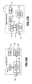
Referring now to FIGS. 11A-11G, various exemplary applications are shown for the variable frequency module. Referring now to FIG. 11A, the variable frequency module can be implemented in high pass filters of a hard disk drive 400. The variable frequency module may be implemented in either or both signal processing and/or control circuits, which are generally identified in FIG. 5A at 402. In some implementations, the signal processing and/or control circuit 402 and/or other circuits (not shown) in the HDD 400 may process data, perform coding and/or encryption, perform calculations, and/or format data that is output to and/or received from a magnetic storage medium 406.
The HDD 400 may communicate with a host device (not shown) such as a computer, mobile computing devices such as personal digital assistants, cellular phones, media or MP3 players and the like, and/or other devices via one or more wired or wireless communication links 408. The HDD 400 may be connected to memory 409 such as random access memory (RAM), low latency nonvolatile memory such as flash memory, read only memory (ROM) and/or other suitable electronic data storage.
Referring now to FIG. 11B, the variable frequency module can be implemented in a digital versatile disc (DVD) drive 410. The variable frequency module may be implemented in high pass filters of signal processing and/or control circuits, which are generally identified in FIG. 11B at 412. The signal processing and/or control circuit 412 and/or other circuits (not shown) in the DVD 410 may process data, perform coding and/or encryption, perform calculations, and/or format data that is read from and/or data written to an optical storage medium 416. In some implementations, the signal processing and/or control circuit 412 and/or other circuits (not shown) in the DVD 410 can also perform other functions such as encoding and/or decoding and/or any other signal processing functions associated with a DVD drive.
The DVD drive 410 may communicate with an output device (not shown) such as a computer, television or other device via one or more wired or wireless communication links 417. The DVD 410 may communicate with mass data storage 418 that stores data in a nonvolatile manner. The mass data storage 418 may include a hard disk drive (HDD). The HDD may have the configuration shown in FIG. 11A. The HDD may be a mini HDD that includes one or more platters having a diameter that is smaller than approximately 1.8″. The DVD 410 may be connected to memory 419 such as RAM, ROM, low latency nonvolatile memory such as flash memory and/or other suitable electronic data storage.
Referring now to FIG. 11C, the variable frequency module can be implemented in high pass filters of a high definition television (HDTV) 420. The device may be implemented in either or both signal processing and/or control circuits, which are generally identified in FIG. 11E at 422. The HDTV 420 receives HDTV input signals in either a wired or wireless format and generates HDTV output signals for a display 426. In some implementations, signal processing circuit and/or control circuit 422 and/or other circuits (not shown) of the HDTV 420 may process data, perform coding and/or encryption, perform calculations, format data and/or perform any other type of HDTV processing that may be required.
The HDTV 420 may communicate with mass data storage 427 that stores data in a nonvolatile manner such as optical and/or magnetic storage devices. At least one HDD may have the configuration shown in FIG. 11A and/or at least one DVD may have the configuration shown in FIG. 11B. The HDD may be a mini HDD that includes one or more platters having a diameter that is smaller than approximately 1.8″. The HDTV 420 may be connected to memory 428 such as RAM, ROM, low latency nonvolatile memory such as flash memory and/or other suitable electronic data storage. The HDTV 420 also may support connections with a WLAN via a WLAN network interface 429.
Referring now to FIG. 11D, the variable frequency module may implement and/or be implemented in high pass filters of a control system of a vehicle 430. In some implementations, the variable frequency module may be implemented in a powertrain control system 432 that receives inputs from one or more sensors such as temperature sensors, pressure sensors, rotational sensors, airflow sensors and/or any other suitable sensors and/or that generates one or more output control signals such as engine operating parameters, transmission operating parameters, and/or other control signals.
The variable frequency module may also be implemented in other control systems 440 of the vehicle 430. The control system 440 may likewise receive signals from input sensors 442 and/or output control signals to one or more output devices 444. In some implementations, the control system 440 may be part of an anti-lock braking system (ABS), a navigation system, a telematics system, a vehicle telematics system, a lane departure system, an adaptive cruise control system, a vehicle entertainment system such as a stereo, DVD, compact disc and the like. Still other implementations are contemplated.
The powertrain control system 432 may communicate with mass data storage 446 that stores data in a nonvolatile manner. The mass data storage 446 may include optical and/or magnetic storage devices for example hard disk drives HDD and/or DVDs. At least one HDD may have the configuration shown in FIG. 11A and/or at least one DVD may have the configuration shown in FIG. 11B. The HDD may be a mini HDD that includes one or more platters having a diameter that is smaller than approximately 1.8″. The powertrain control system 432 may be connected to memory 447 such as RAM, ROM, low latency nonvolatile memory such as flash memory and/or other suitable electronic data storage. The powertrain control system 432 also may support connections with a WLAN via a WLAN network interface 448. The control system 440 may also include mass data storage, memory and/or a WLAN interface (all not shown).
Referring now to FIG. 11E, the variable frequency module can be implemented in high pass filters of a cellular phone 450 that may include a cellular antenna 451. The variable frequency module may implement and/or be implemented in either or both signal processing and/or control circuits, which are generally identified in FIG. 11E at 452. In some implementations, the cellular phone 450 includes a microphone 456, an audio output 458 such as a speaker and/or audio output jack, a display 460 and/or an input device 462 such as a keypad, pointing device, voice actuation and/or other input device. The signal processing and/or control circuits 452 and/or other circuits (not shown) in the cellular phone 450 may process data, perform coding and/or encryption, perform calculations, format data and/or perform other cellular phone functions.
The cellular phone 450 may communicate with mass data storage 464 that stores data in a nonvolatile manner such as optical and/or magnetic storage devices for example hard disk drives HDD and/or DVDs. At least one HDD may have the configuration shown in FIG. 11A and/or at least one DVD may have the configuration shown in FIG. 11B. The HDD may be a mini HDD that includes one or more platters having a diameter that is smaller than approximately 1.8″. The cellular phone 450 may be connected to memory 466 such as RAM, ROM, low latency nonvolatile memory such as flash memory and/or other suitable electronic data storage. The cellular phone 450 also may support connections with a WLAN via a WLAN network interface 468.
Referring now to FIG. 11F, the variable frequency module can be implemented in high pass filters of a set top box 480. The variable frequency module may implement and/or be implemented in either or both signal processing and/or control circuits, which are generally identified in FIG. 5E at 484. The set top box 480 receives signals from a source such as a broadband source and outputs standard and/or high definition audio/video signals suitable for a display 488 such as a television and/or monitor and/or other video and/or audio output devices. The signal processing and/or control circuits 484 and/or other circuits (not shown) of the set top box 480 may process data, perform coding and/or encryption, perform calculations, format data and/or perform any other set top box function.
The set top box 480 may communicate with mass data storage 490 that stores data in a nonvolatile manner. The mass data storage 490 may include optical and/or magnetic storage devices for example hard disk drives HDD and/or DVDs. At least one HDD may have the configuration shown in FIG. 11A and/or at least one DVD may have the configuration shown in FIG. 11B. The HDD may be a mini HDD that includes one or more platters having a diameter that is smaller than approximately 1.8″. The set top box 480 may be connected to memory 494 such as RAM, ROM, low latency nonvolatile memory such as flash memory and/or other suitable electronic data storage. The set top box 480 also may support connections with a WLAN via a WLAN network interface 496.
Referring now to FIG. 11G, the variable frequency module can be implemented in high pass filters of a media player 500. The variable frequency module may implement and/or be implemented in either or both signal processing and/or control circuits, which are generally identified in FIG. 11G at 504. In some implementations, the media player 500 includes a display 507 and/or a user input 508 such as a keypad, touchpad and the like. In some implementations, the media player 500 may employ a graphical user interface (GUI) that typically employs menus, drop down menus, icons and/or a point-and-click interface via the display 507 and/or user input 508. The media player 500 further includes an audio output 509 such as a speaker and/or audio output jack. The signal processing and/or control circuits 504 and/or other circuits (not shown) of the media player 500 may process data, perform coding and/or encryption, perform calculations, format data and/or perform any other media player function.
The media player 500 may communicate with mass data storage 510 that stores data such as compressed audio and/or video content in a nonvolatile manner. In some implementations, the compressed audio files include files that are compliant with MP3 format or other suitable compressed audio and/or video formats. The mass data storage may include optical and/or magnetic storage devices for example hard disk drives HDD and/or DVDs. At least one HDD may have the configuration shown in FIG. 11A and/or at least one DVD may have the configuration shown in FIG. 11B. The HDD may be a mini HDD that includes one or more platters having a diameter that is smaller than approximately 1.8″. The media player 500 may be connected to memory 514 such as RAM, ROM, low latency nonvolatile memory such as flash memory and/or other suitable electronic data storage. The media player 500 also may support connections with a WLAN via a WLAN network interface 516. Still other implementations in addition to those described above are contemplated.
Those skilled in the art can now appreciate from the foregoing description that the broad teachings of the disclosure can be implemented in a variety of forms. Therefore, while this disclosure includes particular examples, the true scope of the disclosure should not be so limited since other modifications will become apparent to the skilled practitioner upon a study of the drawings, the specification and the following claims.

Claims (17)

1. A high pass filter having a cutoff frequency, the high pass filter comprising:
a first amplifier to receive an input signal, the high pass filter to attenuate low frequency signals of the input signal that are below the cutoff frequency;
a second amplifier to provide an output signal, the output signal comprising only high frequency signals of the input signal that are above the cutoff frequency;
a capacitive element coupled in between the first amplifier and the second amplifier; and
a variable frequency module communicating with the capacitive element and including a plurality of resistive paths of the high pass filter,
wherein each resistive path corresponds to a different cutoff frequency for the high pass filter,
wherein the variable frequency module comprises i) a first transistor having a first source/drain region formed in a first well region and ii) a first diode region formed between the first source/drain region and the first well region, wherein a first node of the first diode region is connected to the first source/drain region and a reference node, wherein a second node of the first diode region is connected to the reference node, and wherein the variable frequency module is configured to prevent any leakage current from draining the capacitive element.
2. The high pass filter of claim 1, wherein the variable frequency module comprises:
a resistive element configured to communicate with the capacitive element of the high pass filter.
3. The high pass filter of claim 2, wherein the first transistor further includes:
a first contact region formed in the first well region that is connected to the first source/drain region and the first well region.
4. The high pass filter of claim 3, wherein the first transistor further includes:
a second diode region formed between a second source/drain region and the first well region,
wherein a first node of the second diode region is connected to the second source/drain region, and a second node of the second diode region is connected to the second node of the first diode region and the reference node.
5. The high pass filter of claim 2, further comprising:
a second transistor configured to communicate with the capacitive element and the reference node, the second transistor including:
a second source/drain region formed in a second well region; and
a second diode region formed between the second source/drain region and the second well region,
wherein a first node of the second diode region is connected to the second source/drain region and the reference node, and a second node of the second diode region is connected to the reference node.
6. The high pass filter of claim 5, wherein the second transistor further includes:
a second contact region formed in the second well region, the second well region being connected to the second source/drain region.
7. The high pass filter of claim 6, wherein the second transistor further includes:
a third diode region formed between a third source/drain region and the second well region,
wherein a first node of the third diode region is connected to the third source/drain region, and a second node of the third diode region is connected to the second node of the second diode region and the reference node.
8. The high pass filter of claim 5, wherein the first transistor and the second transistor are fabricated via a twin-well process.
9. The high pass filter of claim 2, wherein the variable frequency module communicates with a reference voltage.
10. The high pass filter of claim 9, wherein the reference node communicates with the reference voltage.
11. The high pass filter of claim 2, wherein the first transistor receives a control signal.
12. The high pass filter of claim 5, wherein the second transistor receives a clock signal.
13. The high pass filter of claim 1, wherein the variable frequency module comprises:
a resistive element configured to communicate with the capacitive element of the high pass filter; and
a first contact region formed in the first well region, wherein the first contact region is connected to the first source/drain region, the first well region, and the reference node.
14. The high pass filter of claim 13,
wherein the resistive element comprises N resistors,
wherein the variable frequency module further comprises N−1 transistors wherein first ends of each of the N resistors are connected together,
wherein second ends of each of the N resistors communicate with a respective one of the N−1 transistors, and
wherein N is an integer greater than or equal to 2.
15. The high pass filter of claim 13, further comprising:
N additional resistive elements configured to communicate with the capacitive element; and
N additional transistors that each include a second source/drain region formed in a second well region, a second diode region formed between the second source/drain region and the second well region, and a second contact region formed in the second well region,
wherein a first end of each of the N additional resistive elements connects to an associated one of the N additional transistors, and a second end of each of the N additional resistive elements connects to an adjacent one of the N additional transistors, and
wherein N is an integer greater than or equal to 1.
16. The high pass filter of claim 13, wherein the first transistor is an NMOS transistor.
17. The high pass filter of claim 13, wherein the first transistor is a PMOS transistor.
US12/413,654 2006-04-21 2009-03-30 Apparatus for attenuating low frequency signals Expired - Fee Related US8076969B1 (en)

Priority Applications (1)

Application Number Priority Date Filing Date Title
US12/413,654 US8076969B1 (en) 2006-04-21 2009-03-30 Apparatus for attenuating low frequency signals

Applications Claiming Priority (3)

Application Number Priority Date Filing Date Title
US79386306P 2006-04-21 2006-04-21
US11/582,906 US7514990B1 (en) 2006-04-21 2006-10-18 Very low frequency high pass filter
US12/413,654 US8076969B1 (en) 2006-04-21 2009-03-30 Apparatus for attenuating low frequency signals

Related Parent Applications (1)

Application Number Title Priority Date Filing Date
US11/582,906 Continuation US7514990B1 (en) 2006-04-21 2006-10-18 Very low frequency high pass filter

Publications (1)

Publication Number Publication Date
US8076969B1 true US8076969B1 (en) 2011-12-13

Family

ID=40512743

Family Applications (2)

Application Number Title Priority Date Filing Date
US11/582,906 Expired - Fee Related US7514990B1 (en) 2006-04-21 2006-10-18 Very low frequency high pass filter
US12/413,654 Expired - Fee Related US8076969B1 (en) 2006-04-21 2009-03-30 Apparatus for attenuating low frequency signals

Family Applications Before (1)

Application Number Title Priority Date Filing Date
US11/582,906 Expired - Fee Related US7514990B1 (en) 2006-04-21 2006-10-18 Very low frequency high pass filter

Country Status (1)

Country Link
US (2) US7514990B1 (en)

Families Citing this family (5)

* Cited by examiner, † Cited by third party
Publication number Priority date Publication date Assignee Title
US11108225B2 (en) 2017-11-08 2021-08-31 Eaton Intelligent Power Limited System, method, and apparatus for power distribution in an electric mobile application using a combined breaker and relay
US11368031B2 (en) 2017-11-08 2022-06-21 Eaton Intelligent Power Limited Power distribution and circuit protection for a mobile application having a high efficiency inverter
CN116742575A (en) 2017-11-08 2023-09-12 伊顿智能动力有限公司 Power distribution unit and fuse management for electric mobile applications
US11070049B2 (en) 2017-11-08 2021-07-20 Eaton Intelligent Power Limited System, method, and apparatus for power distribution in an electric mobile application using a combined breaker and relay
US11682895B2 (en) 2019-02-22 2023-06-20 Eaton Intelligent Power Limited Inverter assembly with integrated coolant coupling port

Citations (5)

* Cited by examiner, † Cited by third party
Publication number Priority date Publication date Assignee Title
US4589136A (en) * 1983-12-22 1986-05-13 AKG Akustische u.Kino-Gerate GmbH Circuit for suppressing amplitude peaks caused by stop consonants in an electroacoustic transmission system
US5760642A (en) 1996-05-07 1998-06-02 Mitsubishi Denki Kabushiki Kaisha Filter circuit using a junction capacitor of a semiconductor
US6496341B1 (en) * 2000-07-13 2002-12-17 United Microelectronics Corp. SOI electrostatic discharge protection circuit
US7317601B2 (en) * 2004-07-29 2008-01-08 United Microelectronics Corp. Electrostatic discharge protection device and circuit thereof
US7440209B1 (en) * 2005-02-15 2008-10-21 Marvell International Ltd. Communications channel with programmable coupling

Patent Citations (5)

* Cited by examiner, † Cited by third party
Publication number Priority date Publication date Assignee Title
US4589136A (en) * 1983-12-22 1986-05-13 AKG Akustische u.Kino-Gerate GmbH Circuit for suppressing amplitude peaks caused by stop consonants in an electroacoustic transmission system
US5760642A (en) 1996-05-07 1998-06-02 Mitsubishi Denki Kabushiki Kaisha Filter circuit using a junction capacitor of a semiconductor
US6496341B1 (en) * 2000-07-13 2002-12-17 United Microelectronics Corp. SOI electrostatic discharge protection circuit
US7317601B2 (en) * 2004-07-29 2008-01-08 United Microelectronics Corp. Electrostatic discharge protection device and circuit thereof
US7440209B1 (en) * 2005-02-15 2008-10-21 Marvell International Ltd. Communications channel with programmable coupling

Also Published As

Publication number Publication date
US7514990B1 (en) 2009-04-07

Similar Documents

Publication Publication Date Title
US7468638B1 (en) Transmit/receive switch device
US7737777B2 (en) Amplifiers with compensation
US7202733B1 (en) Transconductance amplifiers with compensation
US7756486B1 (en) Transmitter and receiver impedance control using shunt switches
US7388531B1 (en) Current steering DAC using thin oxide devices
US8076969B1 (en) Apparatus for attenuating low frequency signals
US8270234B1 (en) Positive and negative voltage level shifter circuit
US7468633B1 (en) Multi-amplifier circuit
US7696820B1 (en) Increasing amplifier bandwidth by positive capacitive feedback
US7589649B1 (en) Apparatus, method, and system for correction of baseline wander
US7375575B1 (en) Method and apparatus for controlled voltage level shifting
US8552788B2 (en) Apparatus and methods for adaptive common-mode level shifting
US7656111B1 (en) Low power preamplifier writer architecture
US7161420B1 (en) Amplifiers with compensation
US8614592B1 (en) High data rate envelope detector for high speed optical storage application
US8891329B2 (en) Input buffer
US7656601B1 (en) Current biasing circuit to reduce MR common mode voltage jumping for MR resistance measurement
KR100888071B1 (en) Differential amplifier with selectable gain
US7893733B1 (en) Voltage driver circuit
US7199656B1 (en) Amplifiers with compensation
EP1783895B1 (en) Transconductance amplifiers with compensation
US7688051B1 (en) Linear regulator with improved power supply rejection
US7504892B1 (en) Charge-pump for phase-locked loop
US7605627B2 (en) Programmable boosting and charge neutralization
US8536874B1 (en) Integrated circuit voltage domain detection system and associated methodology

Legal Events

Date Code Title Description
STCF Information on status: patent grant

Free format text: PATENTED CASE

FPAY Fee payment

Year of fee payment: 4

FEPP Fee payment procedure

Free format text: MAINTENANCE FEE REMINDER MAILED (ORIGINAL EVENT CODE: REM.); ENTITY STATUS OF PATENT OWNER: LARGE ENTITY

LAPS Lapse for failure to pay maintenance fees

Free format text: PATENT EXPIRED FOR FAILURE TO PAY MAINTENANCE FEES (ORIGINAL EVENT CODE: EXP.); ENTITY STATUS OF PATENT OWNER: LARGE ENTITY

STCH Information on status: patent discontinuation

Free format text: PATENT EXPIRED DUE TO NONPAYMENT OF MAINTENANCE FEES UNDER 37 CFR 1.362

FP Lapsed due to failure to pay maintenance fee

Effective date: 20191213

AS Assignment

Owner name: CAVIUM INTERNATIONAL, CAYMAN ISLANDS

Free format text: ASSIGNMENT OF ASSIGNORS INTEREST;ASSIGNOR:MARVELL INTERNATIONAL LTD.;REEL/FRAME:052918/0001

Effective date: 20191231

AS Assignment

Owner name: MARVELL ASIA PTE, LTD., SINGAPORE

Free format text: ASSIGNMENT OF ASSIGNORS INTEREST;ASSIGNOR:CAVIUM INTERNATIONAL;REEL/FRAME:053475/0001

Effective date: 20191231