US8072411B2 - Gate line driving circuit of LCD panel - Google Patents
Gate line driving circuit of LCD panel Download PDFInfo
- Publication number
- US8072411B2 US8072411B2 US12/501,518 US50151809A US8072411B2 US 8072411 B2 US8072411 B2 US 8072411B2 US 50151809 A US50151809 A US 50151809A US 8072411 B2 US8072411 B2 US 8072411B2
- Authority
- US
- United States
- Prior art keywords
- gate line
- switch
- terminal
- electrically connected
- transistor
- Prior art date
- Legal status (The legal status is an assumption and is not a legal conclusion. Google has not performed a legal analysis and makes no representation as to the accuracy of the status listed.)
- Expired - Fee Related, expires
Links
- 230000000087 stabilizing effect Effects 0.000 claims description 49
- 239000010409 thin film Substances 0.000 claims description 11
- 239000004973 liquid crystal related substance Substances 0.000 claims description 4
- 239000003990 capacitor Substances 0.000 description 5
- 230000000694 effects Effects 0.000 description 2
- 238000000034 method Methods 0.000 description 2
- 230000008569 process Effects 0.000 description 2
- 230000008878 coupling Effects 0.000 description 1
- 238000010168 coupling process Methods 0.000 description 1
- 238000005859 coupling reaction Methods 0.000 description 1
- 238000002474 experimental method Methods 0.000 description 1
- 230000005669 field effect Effects 0.000 description 1
- 238000004519 manufacturing process Methods 0.000 description 1
- 239000011159 matrix material Substances 0.000 description 1
- 238000012986 modification Methods 0.000 description 1
- 230000004048 modification Effects 0.000 description 1
- 230000005855 radiation Effects 0.000 description 1
- 238000011160 research Methods 0.000 description 1
- 230000001960 triggered effect Effects 0.000 description 1
Images


Classifications
-
- G—PHYSICS
- G09—EDUCATION; CRYPTOGRAPHY; DISPLAY; ADVERTISING; SEALS
- G09G—ARRANGEMENTS OR CIRCUITS FOR CONTROL OF INDICATING DEVICES USING STATIC MEANS TO PRESENT VARIABLE INFORMATION
- G09G3/00—Control arrangements or circuits, of interest only in connection with visual indicators other than cathode-ray tubes
- G09G3/20—Control arrangements or circuits, of interest only in connection with visual indicators other than cathode-ray tubes for presentation of an assembly of a number of characters, e.g. a page, by composing the assembly by combination of individual elements arranged in a matrix no fixed position being assigned to or needed to be assigned to the individual characters or partial characters
- G09G3/34—Control arrangements or circuits, of interest only in connection with visual indicators other than cathode-ray tubes for presentation of an assembly of a number of characters, e.g. a page, by composing the assembly by combination of individual elements arranged in a matrix no fixed position being assigned to or needed to be assigned to the individual characters or partial characters by control of light from an independent source
- G09G3/36—Control arrangements or circuits, of interest only in connection with visual indicators other than cathode-ray tubes for presentation of an assembly of a number of characters, e.g. a page, by composing the assembly by combination of individual elements arranged in a matrix no fixed position being assigned to or needed to be assigned to the individual characters or partial characters by control of light from an independent source using liquid crystals
- G09G3/3611—Control of matrices with row and column drivers
- G09G3/3674—Details of drivers for scan electrodes
- G09G3/3677—Details of drivers for scan electrodes suitable for active matrices only
-
- G—PHYSICS
- G09—EDUCATION; CRYPTOGRAPHY; DISPLAY; ADVERTISING; SEALS
- G09G—ARRANGEMENTS OR CIRCUITS FOR CONTROL OF INDICATING DEVICES USING STATIC MEANS TO PRESENT VARIABLE INFORMATION
- G09G2300/00—Aspects of the constitution of display devices
- G09G2300/04—Structural and physical details of display devices
- G09G2300/0404—Matrix technologies
- G09G2300/0408—Integration of the drivers onto the display substrate
-
- G—PHYSICS
- G09—EDUCATION; CRYPTOGRAPHY; DISPLAY; ADVERTISING; SEALS
- G09G—ARRANGEMENTS OR CIRCUITS FOR CONTROL OF INDICATING DEVICES USING STATIC MEANS TO PRESENT VARIABLE INFORMATION
- G09G2300/00—Aspects of the constitution of display devices
- G09G2300/04—Structural and physical details of display devices
- G09G2300/0421—Structural details of the set of electrodes
- G09G2300/0426—Layout of electrodes and connections
-
- G—PHYSICS
- G09—EDUCATION; CRYPTOGRAPHY; DISPLAY; ADVERTISING; SEALS
- G09G—ARRANGEMENTS OR CIRCUITS FOR CONTROL OF INDICATING DEVICES USING STATIC MEANS TO PRESENT VARIABLE INFORMATION
- G09G2310/00—Command of the display device
- G09G2310/02—Addressing, scanning or driving the display screen or processing steps related thereto
- G09G2310/0202—Addressing of scan or signal lines
- G09G2310/0205—Simultaneous scanning of several lines in flat panels
-
- G—PHYSICS
- G09—EDUCATION; CRYPTOGRAPHY; DISPLAY; ADVERTISING; SEALS
- G09G—ARRANGEMENTS OR CIRCUITS FOR CONTROL OF INDICATING DEVICES USING STATIC MEANS TO PRESENT VARIABLE INFORMATION
- G09G2310/00—Command of the display device
- G09G2310/02—Addressing, scanning or driving the display screen or processing steps related thereto
- G09G2310/0264—Details of driving circuits
- G09G2310/0291—Details of output amplifiers or buffers arranged for use in a driving circuit
Definitions
- the present invention relates to a LCD panel driving circuit, and particularly to a gate line driving circuit of the LCD panel.
- the TFT circuit comprises a plurality of parallel gate lines, or called scan lines, and a plurality of parallel data lines, or called signal lines.
- the gate lines and the data lines are disposed orthogonally across with each other to form a matrix control circuit. While refreshing a frame, the gate lines are triggered one by one, that is, feeding a high voltage level and then receiving signals from the data lines orthogonally across with one of the gate lines so as to refresh a plurality of corresponding pixels coupling to the gate line. Therefore, the trigger signals of the gate lines are interlaced in order to control the signals of the pixels each.
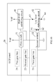
- a driving chip 10 comprises a plurality of output ports, such as a first output port 11 , a second output port 12 and a third output port 13 .
- the LCD panel 20 comprises a plurality of gate lines, such as a first gate line 21 , a second gate line 22 and a third gate line 23 .
- the LCD panel 20 further comprises a plurality of data lines which are disposed orthogonally across with the gate lines.
- the data lines are not shown in the figure since they have no direct relationship with the present invention.
- each gate line is electrically connected to an output port respectively. As shown in FIG.
- the first output port 11 is electrically connected to the first gate line 21
- the second output port 12 is electrically connected to the second gate line 22
- the third output port 13 electrically connected to the third gate line 23 .
- FIG. 2 for a signal waveform chart of the LCD panel driving signals according to the prior art.
- the driving chip 10 sequentially outputs the trigger voltages from each output port to each gate line. Therefore, the driving signal of the first gate line is logical high in the first period T 1 , the driving signal of the second gate line is logical high in the second period T 2 , and the driving signal of the third gate line is logical high in the third period T 3 .
- one objective of the present invention is to provide a gate line driving circuit of LCD panel for reducing the numbers of driving chips needed in a LCD panel.
- a gate line driving circuit which comprises a driving chip which at least comprising a first output port and a second output port, a LCD panel which at least comprising a first gate line, a second gate line and a third gate line, a first switch and a second switch.
- a driving chip which at least comprising a first output port and a second output port
- a LCD panel which at least comprising a first gate line, a second gate line and a third gate line, a first switch and a second switch.
- one terminal of the first gate line is electrically connected to the first output port
- the other terminal of the first gate line is electrically connected to the control terminal of the first switch.
- One terminal of the third gate line is electrically connected to the second output port, and the other terminal of the third gate line is electrically connected to the control terminal of the second switch.
- the input terminal of the first switch is electrically connected to an operating voltage.
- the output terminal of the first switch is electrically connected to the input terminal of the second switch.
- the output terminal of the second switch is electrically connected to a ground point.
- One terminal of the second gate line is electrically connected to between the output terminal of the first switch and the input terminal of the second switch.
- the gate line driving circuit of the invention further comprises a high level stabilizing circuit and a low level stabilizing circuit for increasing the stability of the driving signal of the second gate line of the present invention.
- the high level stabilizing circuit is for stabilizing the logical high signal in the second gate line.
- the low level stabilizing circuit is for stabilizing the logical low signal in the second gate line.
- the gate line driving circuit of the LCD panel of the present invention may comprise the following advantages:
- the gate line driving circuit of the LCD panel is able to use two ports to drive three gate lines, and also can use three ports to drive five gate lines. In other words, the gate line driving circuit of the LCD panel is able to use half the number of output ports comparing with the prior art to achieve the same performance. Therefore, the gate line driving circuit of the LCD panel saves a half of driving chips.
- the gate line driving circuit of the LCD panel needs more TFT, but since the TFT are able to be implemented easily by modifying the photo mask to be used in the process of manufacturing, there would be minimum cost increase.
- FIG. 1 is a schematic view of a LCD panel driving circuit of a prior art.
- FIG. 2 is a signal waveform chart of a LCD panel driving signal of the prior art.
- FIG. 3 is a schematic view of a gate line driving circuit of the present invention.
- FIG. 4 is a signal waveform chart of a gate line driving signal of the present invention.
- FIG. 5 is a schematic view of a gate line driving circuit of an embodiment of the present invention.
- FIG. 6 is a schematic view of a gate line driving circuit of another embodiment of the present invention.
- FIG. 7 is a signal waveform chart of a gate line driving signal of an embodiment of the present invention.
- FIG. 8 is a schematic view of a gate line driving circuit of another embodiment of the present invention.
- FIG. 9 is a signal waveform chart of a gate line driving signal of another embodiment of the present invention.
- FIG. 10 is a schematic view of a gate line driving circuit and a level stabilizing circuit of an embodiment of the present invention.
- FIG. 11 is a schematic view of a low level stabilizing circuit of an embodiment of the present invention.
- FIG. 12 is a schematic view of the high level stabilizing circuit of an embodiment of the present invention.
- FIG. 13 is a schematic view of a level stabilizing circuit of an embodiment of the present invention.
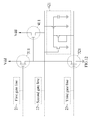
- the gate line driving circuit comprises a driving chip 10 , a LCD panel 20 , a first switch 31 and a second switch 32 .
- the driving chip 10 at least comprises a first output port 11 and a second output port 12 .
- the LCD panel 20 at least comprises a first gate line 21 , a second gate line 22 and a third gate line 23 .
- One terminal of the first gate line 21 is electrically connected to the first output port 11
- the other terminal of the first gate line 21 is electrically connected to the control terminal of the first switch 31 .
- One terminal of the third gate line 23 is electrically connected to the second output port 12 , and the other terminal of the third gate line 23 is electrically connected to the control terminal of the second switch 32 .
- the input terminal of the first switch 31 is electrically connected to an operating voltage Vdd.
- the output terminal of the first switch 31 is electrically connected to the input terminal of the second switch 32 .
- the output terminal of the second switch 32 is electrically connected to a ground point.
- One terminal of the second gate line 22 is electrically connected to between the output terminal of the first switch 31 and the input terminal of the second switch 32 .
- FIG. 4 Please refer to FIG. 4 for a signal waveform chart of a gate line driving signal in accordance with the present invention.
- the driving signal of the first gate line 21 is logical high.
- the first switch 31 receives the driving signal which is logical high from the first gate line 21 , and the driving signal turns on the first switch 31 . Therefore, one terminal of the second gate line 22 electrically connects the operating voltage Vdd.
- the second switch 32 is turned off.
- the driving signals of the first gate line 21 and the second gate line 22 are both logical high in the first period T 1 .
- the first output port 11 provides a logical low signal to the first gate line 21 and causes the first switch 31 to be turned off. Since the second switch 32 is still turned off, the driving signal of the second gate line 22 remains logical high in the second period T 2 .
- the second output port 12 provides a trigger signal to the third gate line 23 and therefore the driving signal of the third gate line 23 is logical high.
- the second switch 32 receives the logical high signal from the third gate line 23 , and therefore is turned on.
- the present invention uses the first switch 31 and the second switch 32 to make the driving signal of the second gate line 22 be logical high in the second period T 2 , and further make the driving signal of the second gate line 22 be logical low in the third period T 3 .
- a first switch 311 is preferably a transistor switch.
- the transistor switch 311 may be a field effect transistor (FET) switch, and particularly be a TFT switch.
- FET field effect transistor
- the transistor switch 311 is able to be implemented by merely modifying the photo mask without increasing any cost.
- a second switch 321 may also be a transistor switch.
- the drawback of the gate line driving circuit of the LCD panel of the present invention is that pixels corresponding to the second gate line 22 might be coupled with error signals while the first gate line 21 triggers the data lines to refresh pixels corresponding to the first gate line 21 in the first period T 1 , and the errors are not corrected until the second period T 2 .
- the refresh rate of the LCD panel is very high, it might not be noticed by the naked eyes, the drawback may be ignored.
- the present invention is able to save almost half of the output ports for the gate line driving circuit driving the hundreds of gate lines of a whole LCD panel 20 . That is, the gate line driving circuit of the LCD panel of the present invention only needs a half of driving chips 10 to achieve the same effect of the prior art.
- FIG. 6 shows a schematic view of a gate line driving circuit of another embodiment of the present invention.
- a first output port 11 and a second output port 12 drive a first gate line 21 and a third gate line 23 , and control a second gate line 22 by using a first switch 31 and a second switch 32 has been described above, and therefore it will not be described in detail for conciseness.
- FIG. 7 for a signal waveform chart of a gate line driving signal of an embodiment of the present invention.
- a driving signal of a third gate line 23 is logical high while a second output port 12 provides a trigger voltage to a third gate line 23 in a third period T 3 .
- a third switch 33 since a third switch 33 receives the logical high signal which comes from the third gate line 23 , the third switch 33 is turned on and one terminal of a fourth gate line 24 is electrically connected to an operating voltage Vdd.
- a third output port 13 since a third output port 13 only provides a logical low signal to a fifth gate line 25 , a fourth switch 34 is turned off. Therefore, the driving signals of the third gate line 23 and the fourth gate line 24 are both logical high in the third period T 3 . And then, the second output port 12 provides a logical low signal to the third gate line 23 and further turns off the third switch 33 in a fourth period T 4 .
- the fourth switch 34 Since the fourth switch 34 is still turned off, the driving signal of the fourth gate line 24 is still logical high in the fourth period T 4 . At last, when the third output port 13 provides a trigger voltage to the fifth gate line 25 in a fifth period T 5 , the driving signal of the fifth gate line 25 is logical high. In the meanwhile, since the fourth switch 34 receives the logical high signal from the fifth gate line 25 , the fourth switch 34 is turned on and then makes one terminal of the fourth gate line 24 electrically connected to the ground point. By this means, the embodiment utilizes the third switch 33 and the fourth switch 34 to ensure the driving signal of the fourth gate line 24 to be logical high in the fourth period T 4 and further to be logical low in the fifth period T 5 .
- the drawback of the embodiment is that when pixels corresponding to the first gate line 21 and the third gate line 23 might be coupled with the signals from the data lines for refreshing, the signals will incorrectly refresh pixels corresponding to the second gate line 22 in the first period T 1 and incorrectly refresh pixels corresponding to the fourth gate line 24 in the third period T 3 . These incorrectly refreshed pixels will not be corrected until the second period T 2 and the fourth period T 4 respectively.
- the refreshing rate is very high, this drawback almost cannot be observed by the naked eyes and therefore may be ignored.
- the gate line driving circuit of the LCD panel of the embodiment only uses three output ports to drive five gate lines. In other words, the embodiment only needs half of the driving chips to achieve the same effect in comparison with the prior art.
- a first switch 311 , second switch 321 , third switch 331 and fourth switch 341 are preferably transistor switches. Wherein, the first switch 321 and the second switch 331 are able to be driven by the same conductive line.
- a driving signal of a second gate line 22 is isolated from an operating voltage Vdd and a ground point via a first switch 31 and a second switch 32 in a second period T 2 . Therefore, the driving signal of the second gate line 22 may be an unstable logical high voltage in the second period T 2 , as shown in a first unstable period P 1 .
- the driving signal of the second gate line 22 is electrically connected to the ground point via the second switch 32 in a third period T 3 , the driving signal of the second gate line 22 still may be floating due to an electromagnetic interference, as shown in a second unstable period P 2 . Therefore, the present invention further provides several embodiments as following to solve the problem mentioned above.
- FIG. 10 for a schematic view of a gate line driving circuit and a level stabilizing circuit of an embodiment in accordance with the present invention.
- the embodiment further provides a high level stabilizing circuit 41 and a low level stabilizing circuit 42 to solve the signal floating problem described in the first unstable period P 1 and the second unstable period P 2 .
- the driving chip and output ports are omitted in the figure.
- the high level stabilizing circuit 41 can be realized simply by a TFT.
- the control terminal of the TFT is electrically connected to the output terminal of a first switch 31 .
- the input terminal of the TFT is electrically connected to an operating voltage Vdd.
- the output terminal of the TFT is electrically connected to a second gate line 22 .
- the driving signal of the second gate line 22 is still logical high and further triggers the high level stabilizing circuit 41 .
- the high level stabilizing circuit 41 makes the second gate line 22 to be electrically connected to the operating voltage Vdd, and further keeps the driving signal of the second gate line 22 to be logical high in the second period T 2 .
- the low level stabilizing circuit 42 is preferably a TFT logical switch.
- the input terminal 63 of the TFT logical switch is electrically connected to the second gate line 22
- the output terminal 64 of the TFT logical switch is electrically connected to a ground point.
- a first control terminal 61 of the TFT logical switch is electrically connected to the second gate line 22
- a second control terminal 62 of the TFT logical switch is electrically connected to a third gate line 23 . Therefore, when the driving signal of the second gate line 22 is logical low and the driving signal of the third gate line 23 is logical high in a third period T 3 , the input terminal 63 of the TFT logical switch electrically conducts the output terminal 64 of the TFT logical switch.
- the low level stabilizing circuit 42 makes the second gate line 22 electrically connect the ground point for eliminating a second unstable period P 2 .
- FIG. 11 a schematic view of a low level stabilizing circuit of an embodiment in accordance with the present invention is shown in FIG. 11 .
- FIG. 11 simply shows a second gate line 22 , a third gate line 23 and a low level stabilizing circuit 421 .
- the low level stabilizing circuit 421 comprises a transistor 51 , a transistor 52 , a transistor 53 and a capacitor 54 .
- the connection relation has been described in FIG. 11 , and will not further be described in detail here.
- the function of the low level stabilizing circuit 421 is described as the following.
- the driving signal of the second gate line 22 is logical high and the driving signal of the third gate line 23 is logical low.
- the transistor 51 is turned on by the second gate line 22 and the transistor 52 is turned off by the third gate line 23 . Therefore, the transistor 53 is turned off and the driving signal of the second gate line 22 is remained in the logical high level and will not be affected by the low level stabilizing circuit 421 in the second period T 2 .
- the driving signal of the second gate line 22 is logical low and the driving signal of the third gate line 23 is logical high.
- the transistor 51 is turned off by the second gate line 22 and the transistor 52 is turned on by the third gate line 23 .
- the third gate line 23 feeds a high level voltage to the gate terminal of the transistor 53 , and the transistor 53 is turned on.
- the second gate line 22 is electrically connected to a ground point via the transistor 53 . Therefore, the voltage level floating problem in a second unstable period P 2 is solved.
- people with ordinary skills in the art may be able to establish the low level stabilizing circuit 421 by the same philosophy in accordance with the present invention but using other structures.
- FIG. 12 a schematic view of a high level stabilizing circuit of an embodiment of the present invention is disclosed in FIG. 12 for ensuring a high level stabilizing circuit 411 will not antagonize a low level stabilizing circuit 421 .
- FIG. 12 the connection relation and functions of each part have been described above, and will not be described again. The following is the operation status of the circuit.
- a driving signal of a first gate line 21 is logical high and causes a transistor switch 311 to be turned on.
- a driving signal of a third gate line 23 is logical low and causes a transistor switch 321 to be turned off.
- the high level stabilizing circuit 411 is turned on, but the low level stabilizing circuit 421 is turned off.
- the driving signals of the first gate line 21 and the third gate line 23 are both logical low, and cause the transistor switch 311 and the transistor switch 321 to be turned off.
- the high level stabilizing circuit 411 is turned on.
- the transistor switch 321 is turned on, and so as to pulls down the voltage level of the second gate line 22 .
- the high level stabilizing circuit 411 is turned off since the gate terminal driving voltage is not high enough. Therefore, the high level stabilizing circuit 411 is turned off, but the low level stabilizing circuit 421 is turned on.
- the level stabilizing circuit comprises a high level stabilizing circuit 412 and a low level stabilizing circuit 422 .
- the high level stabilizing circuit 412 comprises a transistor 55 and a transistor 56 .
- the low level stabilizing circuit 422 comprises a transistor 57 , a transistor 58 , a transistor 59 , a transistor 60 and a capacitor 65 .
- the input terminal and control terminal of the transistor 55 are both electrically connected to a first gate line 21 .
- the output terminal of the transistor 55 is electrically connected to the input terminal of the transistor 57 , the control terminal of the transistor 56 and a second gate line 22 .
- the input terminal of the transistor 56 is electrically connected to the operating voltage Vdd.
- the output terminal of the transistor 56 is electrically connected to the second gate line 22 .
- the transistor 57 , the transistor 58 and the transistor 60 are electrically connected to a ground point via their output terminals.
- One terminal of the capacitor 65 is electrically connected to the control terminals of the transistor 57 and the transistor 60 , the input terminal of the transistor 58 and the output terminal of the transistor 59 .
- the other terminal of the capacitor 65 is electrically connected to the ground point.
- the input terminals of the transistor 57 and the transistor 60 are electrically connected to the second gate line 22 .
- the control terminal and the input terminal of the transistor 59 are electrically connected to a third gate line 23 .
- the driving signal of the first gate line 21 is logical high and causes a transistor switch 311 to be turned on.
- the driving signal of the third gate line 23 is logical low and causes a transistor switch 321 to be turned off.
- the transistor 55 and the transistor 56 are both turned on and cause the driving signal of the second gate line 22 to be logical high.
- the transistor 58 is turned on since the second gate line is in the high voltage level.
- the transistor 59 is turned off since the third gate line 23 is in the low voltage level.
- the transistor 58 transfers the ground voltage to the control terminals of the transistor 57 and the transistor 60 , and further turns off the transistor 57 and the transistor 60 .
- the first gate line 21 and the third gate line 23 are both in the low voltage level.
- the transistor 56 is turned on since the second gate line 22 is still at the high voltage level.
- the driving signal of the second gate line 22 is stably logical high in the second period T 2 .
- the third gate line 23 is at the high voltage level and causes the transistor 59 to be turned on. After the transistor 59 is turned on, the transistor 57 and the transistor 60 are also turned on.
- the capacitor 65 is for stabilizing the high voltage level of the third gate line 23 .
- the transistor 57 and the transistor 60 pull down the voltage level of the second gate line 22 , and cause trigger voltage of the gate terminal of the transistor 56 to be not enough to turn on itself. In other words, the transistor 56 is turned off. Therefore, the high level stabilizing circuit 412 is turned off, and the low level stabilizing circuit 422 is turned on.
Abstract
Description
Claims (7)
Applications Claiming Priority (3)
| Application Number | Priority Date | Filing Date | Title |
|---|---|---|---|
| TW97127488A | 2008-07-18 | ||
| TW097127488A TWI401658B (en) | 2008-07-18 | 2008-07-18 | Gate line driving circuit of lcd panel |
| TW097127488 | 2008-07-18 |
Publications (2)
| Publication Number | Publication Date |
|---|---|
| US20100013804A1 US20100013804A1 (en) | 2010-01-21 |
| US8072411B2 true US8072411B2 (en) | 2011-12-06 |
Family
ID=41529920
Family Applications (1)
| Application Number | Title | Priority Date | Filing Date |
|---|---|---|---|
| US12/501,518 Expired - Fee Related US8072411B2 (en) | 2008-07-18 | 2009-07-13 | Gate line driving circuit of LCD panel |
Country Status (2)
| Country | Link |
|---|---|
| US (1) | US8072411B2 (en) |
| TW (1) | TWI401658B (en) |
Cited By (2)
| Publication number | Priority date | Publication date | Assignee | Title |
|---|---|---|---|---|
| US20110157168A1 (en) * | 2009-12-31 | 2011-06-30 | Broadcom Corporation | Three-dimensional display system with adaptation based on viewing reference of viewer(s) |
| US9247286B2 (en) | 2009-12-31 | 2016-01-26 | Broadcom Corporation | Frame formatting supporting mixed two and three dimensional video data communication |
Families Citing this family (2)
| Publication number | Priority date | Publication date | Assignee | Title |
|---|---|---|---|---|
| CN103293813B (en) * | 2013-05-29 | 2015-07-15 | 北京京东方光电科技有限公司 | Pixel driving circuit, driving method thereof, array substrate and display device |
| WO2020084770A1 (en) | 2018-10-26 | 2020-04-30 | 三菱電機株式会社 | Numerical control device and numerical control method |
Citations (2)
| Publication number | Priority date | Publication date | Assignee | Title |
|---|---|---|---|---|
| US7602368B2 (en) * | 2004-07-05 | 2009-10-13 | Himax Technologies, Inc. | Reset device and method for a scan driver |
| US7796106B2 (en) * | 2006-01-13 | 2010-09-14 | Samsung Electronics Co., Ltd. | Liquid crystal display |
Family Cites Families (1)
| Publication number | Priority date | Publication date | Assignee | Title |
|---|---|---|---|---|
| TW200615890A (en) * | 2004-11-03 | 2006-05-16 | Wintek Corp | Gate drive circuit layout method of display panel |
-
2008
- 2008-07-18 TW TW097127488A patent/TWI401658B/en not_active IP Right Cessation
-
2009
- 2009-07-13 US US12/501,518 patent/US8072411B2/en not_active Expired - Fee Related
Patent Citations (2)
| Publication number | Priority date | Publication date | Assignee | Title |
|---|---|---|---|---|
| US7602368B2 (en) * | 2004-07-05 | 2009-10-13 | Himax Technologies, Inc. | Reset device and method for a scan driver |
| US7796106B2 (en) * | 2006-01-13 | 2010-09-14 | Samsung Electronics Co., Ltd. | Liquid crystal display |
Cited By (15)
| Publication number | Priority date | Publication date | Assignee | Title |
|---|---|---|---|---|
| US20110157168A1 (en) * | 2009-12-31 | 2011-06-30 | Broadcom Corporation | Three-dimensional display system with adaptation based on viewing reference of viewer(s) |
| US20110157167A1 (en) * | 2009-12-31 | 2011-06-30 | Broadcom Corporation | Coordinated driving of adaptable light manipulator, backlighting and pixel array in support of adaptable 2d and 3d displays |
| US20110164115A1 (en) * | 2009-12-31 | 2011-07-07 | Broadcom Corporation | Transcoder supporting selective delivery of 2d, stereoscopic 3d, and multi-view 3d content from source video |
| US8922545B2 (en) | 2009-12-31 | 2014-12-30 | Broadcom Corporation | Three-dimensional display system with adaptation based on viewing reference of viewer(s) |
| US8964013B2 (en) | 2009-12-31 | 2015-02-24 | Broadcom Corporation | Display with elastic light manipulator |
| US8988506B2 (en) | 2009-12-31 | 2015-03-24 | Broadcom Corporation | Transcoder supporting selective delivery of 2D, stereoscopic 3D, and multi-view 3D content from source video |
| US9019263B2 (en) * | 2009-12-31 | 2015-04-28 | Broadcom Corporation | Coordinated driving of adaptable light manipulator, backlighting and pixel array in support of adaptable 2D and 3D displays |
| US9049440B2 (en) | 2009-12-31 | 2015-06-02 | Broadcom Corporation | Independent viewer tailoring of same media source content via a common 2D-3D display |
| US9066092B2 (en) | 2009-12-31 | 2015-06-23 | Broadcom Corporation | Communication infrastructure including simultaneous video pathways for multi-viewer support |
| US9124885B2 (en) | 2009-12-31 | 2015-09-01 | Broadcom Corporation | Operating system supporting mixed 2D, stereoscopic 3D and multi-view 3D displays |
| US9143770B2 (en) | 2009-12-31 | 2015-09-22 | Broadcom Corporation | Application programming interface supporting mixed two and three dimensional displays |
| US9204138B2 (en) | 2009-12-31 | 2015-12-01 | Broadcom Corporation | User controlled regional display of mixed two and three dimensional content |
| US9247286B2 (en) | 2009-12-31 | 2016-01-26 | Broadcom Corporation | Frame formatting supporting mixed two and three dimensional video data communication |
| US9654767B2 (en) | 2009-12-31 | 2017-05-16 | Avago Technologies General Ip (Singapore) Pte. Ltd. | Programming architecture supporting mixed two and three dimensional displays |
| US9979954B2 (en) | 2009-12-31 | 2018-05-22 | Avago Technologies General Ip (Singapore) Pte. Ltd. | Eyewear with time shared viewing supporting delivery of differing content to multiple viewers |
Also Published As
| Publication number | Publication date |
|---|---|
| TW201005711A (en) | 2010-02-01 |
| US20100013804A1 (en) | 2010-01-21 |
| TWI401658B (en) | 2013-07-11 |
Similar Documents
| Publication | Publication Date | Title |
|---|---|---|
| US9659540B1 (en) | GOA circuit of reducing power consumption | |
| US9779682B2 (en) | GOA circuit with forward-backward scan function | |
| US7936331B2 (en) | Shift register and a display device including the shift register | |
| KR101878380B1 (en) | Scanning drive circuit and organic light-emitting display | |
| US9230498B2 (en) | Driving circuit and method of driving liquid crystal panel and liquid crystal display | |
| US20160372063A1 (en) | Shift register unit and driving method thereof, gate driving circuit and display apparatus | |
| US20090289878A1 (en) | Liquid crystal display device and driving method thereof | |
| US20170243555A1 (en) | Charging scan and charge sharing scan double output goa circuit | |
| US20160351152A1 (en) | Goa circuit based on oxide semiconductor thin film transistor | |
| US11211024B2 (en) | Display panel and display device | |
| US10665194B1 (en) | Liquid crystal display device and driving method thereof | |
| EP2511754A1 (en) | Pixel circuit and display apparatus | |
| US10115338B2 (en) | Driving circuit and display device using the same | |
| US8587506B2 (en) | Display device | |
| WO2015192528A1 (en) | Pixel circuit and display device | |
| US8072411B2 (en) | Gate line driving circuit of LCD panel | |
| WO2020051992A1 (en) | Driving circuit, driving method, and display panel | |
| US8872747B2 (en) | LCD panel with structure of Cs-on-gate type storage capacitor connecting with thin film transistor | |
| US11468862B2 (en) | Drive circuit and method for display apparatus | |
| US9024860B2 (en) | Scanner, electro-optical panel, electro-optical display device and electronic apparatus | |
| US20130162508A1 (en) | Driving Circuit of a Liquid Crystal Panel and an LCD | |
| WO2020215589A1 (en) | Goa circuit and display panel | |
| US10777161B2 (en) | Array substrate, liquid crystal display panel and display device | |
| CN214226481U (en) | GIP circuit for improving output waveform stability | |
| EP3719788A1 (en) | Liquid crystal display panel and eoa module thereof |
Legal Events
| Date | Code | Title | Description |
|---|---|---|---|
| AS | Assignment |
Owner name: HANNSTAR DISPLAY CORP.,TAIWAN Free format text: ASSIGNMENT OF ASSIGNORS INTEREST;ASSIGNORS:CHEN, YAN-JOU;WANG, HUNG-JEN;REEL/FRAME:022943/0776 Effective date: 20090619 Owner name: HANNSTAR DISPLAY CORP., TAIWAN Free format text: ASSIGNMENT OF ASSIGNORS INTEREST;ASSIGNORS:CHEN, YAN-JOU;WANG, HUNG-JEN;REEL/FRAME:022943/0776 Effective date: 20090619 |
|
| ZAAA | Notice of allowance and fees due |
Free format text: ORIGINAL CODE: NOA |
|
| ZAAB | Notice of allowance mailed |
Free format text: ORIGINAL CODE: MN/=. |
|
| STCF | Information on status: patent grant |
Free format text: PATENTED CASE |
|
| FPAY | Fee payment |
Year of fee payment: 4 |
|
| MAFP | Maintenance fee payment |
Free format text: PAYMENT OF MAINTENANCE FEE, 8TH YEAR, LARGE ENTITY (ORIGINAL EVENT CODE: M1552); ENTITY STATUS OF PATENT OWNER: LARGE ENTITY Year of fee payment: 8 |
|
| FEPP | Fee payment procedure |
Free format text: MAINTENANCE FEE REMINDER MAILED (ORIGINAL EVENT CODE: REM.); ENTITY STATUS OF PATENT OWNER: LARGE ENTITY |
|
| LAPS | Lapse for failure to pay maintenance fees |
Free format text: PATENT EXPIRED FOR FAILURE TO PAY MAINTENANCE FEES (ORIGINAL EVENT CODE: EXP.); ENTITY STATUS OF PATENT OWNER: LARGE ENTITY |
|
| STCH | Information on status: patent discontinuation |
Free format text: PATENT EXPIRED DUE TO NONPAYMENT OF MAINTENANCE FEES UNDER 37 CFR 1.362 |
|
| FP | Lapsed due to failure to pay maintenance fee |
Effective date: 20231206 |