US8072270B2 - CMOS RF power amplifier with LDMOS bias circuit for large supply voltages - Google Patents
CMOS RF power amplifier with LDMOS bias circuit for large supply voltages Download PDFInfo
- Publication number
- US8072270B2 US8072270B2 US12/430,645 US43064509A US8072270B2 US 8072270 B2 US8072270 B2 US 8072270B2 US 43064509 A US43064509 A US 43064509A US 8072270 B2 US8072270 B2 US 8072270B2
- Authority
- US
- United States
- Prior art keywords
- transistor
- bias
- circuitry
- current
- voltage
- Prior art date
- Legal status (The legal status is an assumption and is not a legal conclusion. Google has not performed a legal analysis and makes no representation as to the accuracy of the status listed.)
- Expired - Fee Related, expires
Links
Images


Classifications
-
- H—ELECTRICITY
- H03—ELECTRONIC CIRCUITRY
- H03F—AMPLIFIERS
- H03F1/00—Details of amplifiers with only discharge tubes, only semiconductor devices or only unspecified devices as amplifying elements
- H03F1/08—Modifications of amplifiers to reduce detrimental influences of internal impedances of amplifying elements
- H03F1/22—Modifications of amplifiers to reduce detrimental influences of internal impedances of amplifying elements by use of cascode coupling, i.e. earthed cathode or emitter stage followed by earthed grid or base stage respectively
- H03F1/223—Modifications of amplifiers to reduce detrimental influences of internal impedances of amplifying elements by use of cascode coupling, i.e. earthed cathode or emitter stage followed by earthed grid or base stage respectively with MOSFET's
-
- H—ELECTRICITY
- H03—ELECTRONIC CIRCUITRY
- H03F—AMPLIFIERS
- H03F1/00—Details of amplifiers with only discharge tubes, only semiconductor devices or only unspecified devices as amplifying elements
- H03F1/02—Modifications of amplifiers to raise the efficiency, e.g. gliding Class A stages, use of an auxiliary oscillation
- H03F1/0205—Modifications of amplifiers to raise the efficiency, e.g. gliding Class A stages, use of an auxiliary oscillation in transistor amplifiers
- H03F1/0261—Modifications of amplifiers to raise the efficiency, e.g. gliding Class A stages, use of an auxiliary oscillation in transistor amplifiers with control of the polarisation voltage or current, e.g. gliding Class A
-
- H—ELECTRICITY
- H03—ELECTRONIC CIRCUITRY
- H03F—AMPLIFIERS
- H03F1/00—Details of amplifiers with only discharge tubes, only semiconductor devices or only unspecified devices as amplifying elements
- H03F1/52—Circuit arrangements for protecting such amplifiers
-
- H—ELECTRICITY
- H03—ELECTRONIC CIRCUITRY
- H03F—AMPLIFIERS
- H03F3/00—Amplifiers with only discharge tubes or only semiconductor devices as amplifying elements
- H03F3/189—High-frequency amplifiers, e.g. radio frequency amplifiers
- H03F3/19—High-frequency amplifiers, e.g. radio frequency amplifiers with semiconductor devices only
- H03F3/195—High-frequency amplifiers, e.g. radio frequency amplifiers with semiconductor devices only in integrated circuits
-
- H—ELECTRICITY
- H03—ELECTRONIC CIRCUITRY
- H03F—AMPLIFIERS
- H03F3/00—Amplifiers with only discharge tubes or only semiconductor devices as amplifying elements
- H03F3/20—Power amplifiers, e.g. Class B amplifiers, Class C amplifiers
- H03F3/24—Power amplifiers, e.g. Class B amplifiers, Class C amplifiers of transmitter output stages
-
- H—ELECTRICITY
- H03—ELECTRONIC CIRCUITRY
- H03F—AMPLIFIERS
- H03F2200/00—Indexing scheme relating to amplifiers
- H03F2200/18—Indexing scheme relating to amplifiers the bias of the gate of a FET being controlled by a control signal
Definitions
- This invention relates generally to electronic circuitry and more particularly to bias voltage circuitry.
- Communication systems are known to support wireless and wire lined communications between wireless and/or wire lined communication devices. Such communication systems range from national and/or international cellular telephone systems to the Internet to point-to-point in-home wireless networks. Each type of communication system is constructed, and hence operates, in accordance with one or more communication standards.
- wireless communication systems may operate in accordance with one or more standards including, but not limited to, IEEE 802.11x, Bluetooth, wireless wide area networks (e.g., WiMAX), advanced mobile phone services (AMPS), digital AMPS, global system for mobile communications (GSM), North American code division multiple access (CDMA), Wideband CDMA, local multi-point distribution systems (LMDS), multi-channel-multi-point distribution systems (MMDS), radio frequency identification (RFID), Enhanced Data rates for GSM Evolution (EDGE), General Packet Radio Service (GPRS), and many others.
- IEEE 802.11x Bluetooth
- wireless wide area networks e.g., WiMAX
- AMPS advanced mobile phone services
- AMPS advanced mobile phone services
- GSM global system for mobile communications
- CDMA North American code division multiple access
- LMDS local multi-point distribution systems
- MMDS multi-channel-multi-point distribution systems
- RFID radio frequency identification
- EDGE Enhanced Data rates for GSM Evolution
- GPRS General Packet Radio Service
- a wireless communication device such as a cellular telephone, two-way radio, personal digital assistant (PDA), personal computer (PC), laptop computer, home entertainment equipment, RFID reader, RFID tag, et cetera communicates directly or indirectly with other wireless communication devices.
- PDA personal digital assistant
- PC personal computer
- laptop computer home entertainment equipment
- RFID reader RFID tag
- et cetera communicates directly or indirectly with other wireless communication devices.
- the participating wireless communication devices tune their receivers and transmitters to the same channel or channels (e.g., one of the plurality of radio frequency (RF) carriers of the wireless communication system or a particular RF frequency for some systems) and communicate over that channel(s).
- RF radio frequency
- each wireless communication device communicates directly with an associated base station (e.g., for cellular services) and/or an associated access point (e.g., for an in-home or in-building wireless network) via an assigned channel.
- an associated base station e.g., for cellular services
- an associated access point e.g., for an in-home or in-building wireless network
- the associated base stations, and/or associated access points communicate with each other directly, via a system controller, via the public switch telephone network, via the Internet, and/or via some other wide area network.
- each wireless communication device For each wireless communication device to participate in wireless communications, it includes a built-in radio transceiver (i.e., receiver and transmitter) or is coupled to an associated radio transceiver (e.g., a station for in-home and/or in-building wireless communication networks, RF modem, etc.).
- the receiver is coupled to an antenna and includes a low noise amplifier, one or more intermediate frequency stages, a filtering stage, and a data recovery stage.
- the low noise amplifier receives inbound RF signals via the antenna and amplifies then.
- the one or more intermediate frequency stages mix the amplified RF signals with one or more local oscillations to convert the amplified RF signal into baseband signals or intermediate frequency (IF) signals.
- IF intermediate frequency
- the filtering stage filters the baseband signals or the IF signals to attenuate unwanted out of band signals to produce filtered signals.
- the data recovery stage recovers raw data from the filtered signals in accordance with the particular wireless communication standard.
- the transmitter includes a data modulation stage, one or more intermediate frequency stages, and a power amplifier.
- the data modulation stage converts raw data into baseband signals in accordance with a particular wireless communication standard.
- the one or more intermediate frequency stages mix the baseband signals with one or more local oscillations to produce RF signals.
- the power amplifier amplifies the RF signals prior to transmission via an antenna.
- the RF power amplifier In wireless communication devices, the RF power amplifier is often required to provide a high swing at its output. The RF power amplifier must also be very linear in its operation and also use as little power as possible. These competing goals are very difficult to meet. Conventional integrated circuitry is voltage limited due to device dimensions. Thus, the RF power amplifier is thus limited in its operational swing due to the voltage level at which it can operate. Further, when battery voltage exceeds the voltage limitation of the integrated circuit, a voltage regulator is required to generate a voltage that is usable by the integrated circuit.
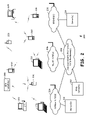
- FIG. 1 is a system diagram illustrating a plurality of devices having bias circuitry constructed according one or more embodiments of the present invention
- FIG. 2 is a system diagram illustrating a wireless communication system constructed and operating according to one or more embodiments of the present invention
- FIG. 3 is a schematic block diagram illustrating a wireless communication device that includes a host device and an associated radio;
- FIG. 4 is a block diagram illustrating a Radio Frequency (RF) cascode power amplifier constructed according to one or more embodiments of the present invention
- FIG. 5 is a circuit diagram illustrating bias circuitry constructed according to one or more embodiments of the present invention.
- FIG. 6A is a block diagram illustrating a RF cascode power amplifier constructed according to one or more embodiments of the present invention.
- FIG. 6B is a block diagram illustrating another RF cascode power amplifier constructed according to one or more embodiments of the present invention.
- FIG. 7 is a block diagram illustrating a differential embodiment of an RF cascode power amplifier constructed according to one or more embodiments of the present invention.
- FIG. 1 is a system diagram illustrating a plurality of devices having bias circuitry constructed according one or more embodiments of the present invention.
- Such devices include portable gaming device 102 , cellular phone 106 , wireless local area network (WLAN) device 112 , wireless wide area network (WWAN) device 120 , personal data assistant (PDA) 116 , and wireless personal area network (WPAN) device 126 .
- WLAN wireless local area network
- WWAN wireless wide area network
- PDA personal data assistant
- WPAN wireless personal area network
- These devices 102 , 106 , 112 , 120 , 116 , and 126 include bias circuitry 104 , 108 , 114 , 124 , 118 , and 128 , respectively.
- FIGS. 1 is a system diagram illustrating a plurality of devices having bias circuitry constructed according one or more embodiments of the present invention.
- Such devices include portable gaming device 102 , cellular phone 106 , wireless local area network (WLAN) device 11
- the bias circuitry may be employed to provide one or more bias voltages to a radio frequency (RF) power amplifier of a wireless device.
- RF radio frequency
- the bias circuitry of the present invention can be used in any situation in which a bias voltage is produced within a device or within an integrated circuit contained within such device.
- the bias circuitry of the present invention may be coupled between a battery voltage node and ground.
- the bias circuitry of the present invention is constructed to withstand higher battery voltages used by some devices without voltage breakdown.
- laterally diffused metal oxide silicon (LDMOS) devices are used in the bias circuitry.
- LDMOS devices have relatively high voltage breakdown capabilities as compared to normal gate or normal transistors formed in an integrated circuit.
- the structure of LDMOS devices is generally known and is not described further herein other than with regard to the present invention.
- FIG. 2 is a system diagram illustrating a wireless communication system constructed and operating according to one or more embodiments of the present invention.
- the wireless communication system 200 of FIG. 2 includes a communication infrastructure and a plurality of wireless devices.
- the communication infrastructure includes one or more cellular networks 204 , one or more wireless local area networks (WLANs) 206 , and one or more wireless wide area networks (WWANs) 208 .
- the cellular networks 204 , WLANs 206 , WWANs 208 all typically couple to one or more backbone networks.
- the backbone networks 202 may include the Internet, the Worldwide Web, one or more public switched telephone network backbones, one or more cellular network backbones, one or more private network backbones and/or other types of backbones that support communications with the various wireless network infrastructures 204 , 206 , and 208 .
- Server computers may couple to these various network infrastructures.
- server computer 210 couples to cellular network 204
- web server 212 couples to the Internet/WWW/PSTN/Cell network 202
- server 214 couples to WWAN network 208 .
- Other devices may couple to these networks as well in various other constructs.
- Each of the cellular networks 204 , WLANs 206 , and WWANs 208 support wireless communications with wireless devices in various wireless spectra and according to various communication protocol standards.
- the cellular network 204 may support wireless communications with wireless devices within the 800 MHz band and the 1800 MHz band, and/or other Radio Frequency (RF) bands that are allocated for cellular network communications.
- the cellular network 204 may support GSM, EDGE, GPRS, 3G, CDMA, TDMA, and/or various other standardized communications. Of course, these are examples only and should not be considered to limit the spectra or operations used by such cellular networks.
- the WLANs 206 typically operate within the Industrial, Scientific, and Medical (ISM) bands that include the 2.4 GHz and 5.8 GHz bands.
- ISM Industrial, Scientific, and Medical
- the ISM bands include other frequencies as well that support other types of wireless communications, such bands including the 6.78 MHz, 13.56 MHz, 27.12 MHz, 40.68 MHz, 433.92 MHz, 915 MHz, 24.125 GHz, 61.25 GHz, 122.5 GHz, and 245 GHz bands.
- the WWANs networks 208 may operate within differing RF spectra based upon that which is allocated at any particular locale. Device to device communications may be serviced in one of these frequency bands as well.
- the wireless network infrastructures 204 , 206 , and 208 support communications to and from wireless devices 216 , 218 , 222 , 224 , 226 , 228 , 230 , 232 , and/or 236 .
- wireless devices include laptop computers 216 and 218 , desktop computers 222 and 224 , cellular telephones 226 and 228 , portable beta terminals 230 , 232 , and 236 .
- differing types of devices may be considered wireless devices within the context of the scope of the present invention. For example, automobiles themselves having cellular interfaces would be considered wireless devices according to the present invention.
- wireless devices may include Global Positioning System (GPS) receiving capability to receive positioning signals from multiple GPS satellites 250 .
- GPS Global Positioning System
- the wireless devices 216 - 236 may support peer-to-peer communications as well, such peer-to-peer communications not requiring the support of a wireless network infrastructure. For example, these devices may communicate with each other in a 60 GHz spectrum, may use a peer-to-peer communications within a WLAN spectrum, for example, or may use other types of peer-to-peer communications. For example, within the ISM spectra, wireless devices may communicate according to Bluetooth protocol or any of the various available WLAN protocols supported by IEEE802.11x, for example.
- each of the wireless devices 216 - 236 illustrated in FIG. 2 includes baseband processing circuitry, Radio Frequency (RF) transceiver, and at least one antenna.
- the RF transceiver includes an RF power amplifier having bias circuitry constructed and operating according to the present invention.
- the bias circuitry and/or the RF power amplifiers of these devices are efficient and able to operate at relatively high battery voltages without requiring a voltage regulator.
- FIG. 3 is a schematic block diagram illustrating a wireless communication device that includes a host device and an associated radio.
- the radio 360 is a built-in component.
- the radio 360 may be built-in or may be an externally coupled component that couples to the host device 302 via a communication link, e.g., PCI interface, PCMCIA interface, USB interface, or another type of interface.
- the host device 302 includes a processing module 350 , memory 352 , radio interface 354 , input interface 358 , and output interface 356 .
- the processing module 350 and memory 352 execute the corresponding instructions that are typically done by the host device. For example, for a cellular telephone host device, the processing module 350 performs the corresponding communication functions in accordance with a particular cellular telephone standard.
- the radio interface 354 allows data to be received from and sent to the radio 360 .
- the radio interface 354 For data received from the radio 360 (e.g., inbound data), the radio interface 354 provides the data to the processing module 350 for further processing and/or routing to the output interface 356 .
- the output interface 356 provides connectivity to an output display device such as a display, monitor, speakers, et cetera, such that the received data may be displayed.
- the radio interface 354 also provides data from the processing module 350 to the radio 360 .
- the processing module 350 may receive the outbound data from an input device such as a keyboard, keypad, microphone, et cetera via the input interface 358 or generate the data itself.
- the processing module 350 may perform a corresponding host function on the data and/or route it to the radio 360 via the radio interface 354 .
- Radio 360 includes a host interface 362 , baseband processing circuitry/baseband processing module 364 , an analog-to-digital converter (ADC) 366 , a filtering/gain/attenuation module 368 , an IF mixing down conversion stage 370 , a receiver filter 371 , a low noise amplifier (LNA) 372 , a transmitter/receiver switch 373 , a local oscillation module 374 , memory 375 , a digital-to-analog converter (DAC) 378 , a filtering/gain/attenuation module 380 , an IF mixing up conversion stage 382 , a power amplifier (PA) 384 , a transmitter filter module 385 , and one or more antennas 386 .
- ADC analog-to-digital converter
- PA power amplifier
- the antenna 386 may be a single antenna that is shared by the transmit and receive paths as regulated by the Tx/Rx switch 373 , or may include separate antennas for the transmit path and receive path.
- the antenna implementation will depend on the particular standard to which the wireless communication device is compliant and the particular design of the device.
- the baseband processing circuitry 364 executes digital receiver functions and digital transmitter functions.
- the digital receiver functions include, but are not limited to, digital intermediate frequency to baseband conversion, demodulation, constellation demapping, decoding, and/or descrambling.
- the digital transmitter functions include, but are not limited to, scrambling, encoding, constellation mapping, modulation, and/or digital baseband to IF conversion.
- the baseband processing circuitry 364 may be implemented using a shared processing device, individual processing devices, or a plurality of processing devices.
- Such a processing device may be a microprocessor, micro-controller, digital signal processor, microcomputer, central processing unit, field programmable gate array, programmable logic device, state machine, logic circuitry, analog circuitry, digital circuitry, and/or any device that manipulates signals (analog and/or digital) based on operational instructions.
- the memory 375 may be a single memory device or a plurality of memory devices.
- Such a memory device may be a read-only memory, random access memory, volatile memory, non-volatile memory, static memory, dynamic memory, flash memory, and/or any device that stores digital information.
- the baseband processing circuitry 364 implements one or more of its functions via a state machine, analog circuitry, digital circuitry, and/or logic circuitry
- the memory storing the corresponding operational instructions is embedded with the circuitry comprising the state machine, analog circuitry, digital circuitry, and/or logic circuitry.
- the memory 375 stores, and the baseband processing circuitry 364 executes, operational instructions that facilitate functionality of the device.
- the radio 360 receives outbound data 394 from the host device via the host interface 362 .
- the host interface 362 routes the outbound data 394 to the baseband processing circuitry 364 , which processes the outbound data 394 in accordance with a particular wireless communication standard (e.g., Cellular, WiMAX, IEEE802.11a, IEEE802.11b, IEEE802.11g, IEEE802.11n, Bluetooth, et cetera) to produce digital transmission formatted data/outgoing baseband signal 396 .
- the digital transmission formatted data 396 will be a digital base-band signal or a digital low IF signal, where the low IF typically will be in the frequency range of one hundred kilohertz to a few megahertz.
- the digital-to-analog converter 378 converts the digital transmission formatted data 396 from the digital domain to the analog domain.
- the filtering/gain/attenuation module 380 filters and/or adjusts the gain of the analog signal prior to providing it to the IF mixing stage 382 .
- the IF mixing stage 382 directly or via multiple conversion steps (super heterodyne) converts the analog baseband or low IF signal into an RF signal based on a transmitter local oscillation 383 provided by local oscillation module 374 .
- the power amplifier (PA) 384 amplifies the RF signal to produce outbound RF signal 398 , which is filtered by the transmitter filter module 385 .
- the antenna 386 transmits the outbound RF signal 398 to a targeted device such as a base station, an access point, and/or another wireless communication device.
- the radio 360 also receives an inbound RF signal 388 via the antenna 386 , which was transmitted by a base station, an access point, or another wireless communication device.
- the antenna 386 provides the inbound RF signal 388 to the receiver filter module 371 via the Tx/Rx switch 373 , where the Rx filter 371 band pass filters the inbound RF signal 388 .
- the Rx filter 371 provides the filtered RF signal to low noise amplifier (LNA) 372 , which amplifies the signal 388 to produce an amplified inbound RF signal.
- LNA low noise amplifier
- the low noise amplifier 372 provides the amplified inbound RF signal to the IF mixing module 370 , which directly converts the amplified inbound RF signal into an inbound low IF signal or baseband signal based on a receiver local oscillation 381 provided by local oscillation module 374 .
- the down conversion module 370 provides the inbound low IF signal or baseband signal to the filtering/gain/attenuation module 368 .
- the filtering/gain/attenuation module 368 may be implemented in accordance with the teachings of the present invention to filter and/or attenuate the inbound low IF signal or the inbound baseband signal to produce a filtered inbound signal.
- the analog-to-digital converter 366 converts the filtered inbound signal from the analog domain to the digital domain to produce digital reception formatted data/incoming baseband signal 390 .
- the baseband processing circuitry 364 decodes, descrambles, demaps, and/or demodulates the digital reception formatted data 390 to recapture inbound data 392 in accordance with the particular wireless communication standard being implemented by radio 360 .
- the host interface 362 provides the recaptured inbound data 392 to the host device 28 - 32 via the radio interface 354 .
- the wireless communication device of FIG. 3 may be implemented using one or more integrated circuits.
- the host device may be implemented on one integrated circuit
- the baseband processing circuitry 364 , and memory 375 may be implemented on a second integrated circuit
- the remaining components of the radio 360 less the antenna(s) 386 , may be implemented on a third integrated circuit.
- the radio 360 may be implemented on a single integrated circuit.
- the processing module 350 of the host device and the baseband processing circuitry 364 may be a common processing device implemented on a single integrated circuit.
- the memory 352 and memory 375 may be implemented on a single integrated circuit and/or on the same integrated circuit as the common processing modules of processing module 350 and the baseband processing circuitry 364 .
- the radio 360 and/or the host device components 302 may include bias circuitry constructed according to one or more aspects of the present invention.
- the bias circuitry of embodiments of the present invention is able to couple to a relatively high battery voltage source node, without the requirement of a voltage regulator.
- an RF PA 384 may also be constructed to operate at the relatively high voltage battery source node, providing improved performance in amplifying RF signals for transmission.
- the bias circuitry may also operate at the relatively high voltage battery node and provide correct bias voltage(s) to the RF PA 384 .
- FIG. 4 is a block diagram illustrating a RF cascode power amplifier constructed according to one or more embodiments of the present invention.
- the RF power amplifier includes an amplifier portion 402 having a transconductance stage 408 and a cascade stage 410 .
- the transconductance stage 408 has a transconductance device with an RF signal input operable to receive the RF input signal P in .
- the cascode stage 410 has at least one cascode transistor and is coupled in series with the transconductance stage 408 between a battery voltage node 404 and ground 406 .
- the cascode stage 410 has an RF signal output that produces the signal P out .
- the cascode stage 410 has at least one bias input that is applied to a gate of the at least one cascode transistor. As illustrated in FIG. 4 , the at least one bias input receives one or more bias voltages, the number of which depends upon the number of cascode transistors included in the cascode stage 410 .
- the RF power amplifier of FIG. 4 further includes bias circuitry 412 .
- the bias circuitry 412 couples between the battery voltage node 404 and ground 406 .
- the bias circuitry 412 applies a bias voltage or voltages to the at least one bias input of the cascode stage 410 .
- the battery voltage upon which bias circuitry 412 determines and sets the bias voltage(s) is represented by V Batt present at the battery voltage node 404 .
- the bias voltage(s) is/are based upon the voltage at the battery voltage node 404 , which also serves as the signal output node to produce signal P out .
- FIG. 5 is a circuit diagram illustrating bias circuitry constructed according to one or more embodiments of the present invention.
- the bias circuitry 500 may be employed with any of the various devices illustrated in FIGS. 1 , 2 , and 3 and that will be described subsequently with reference to FIGS. 6A-7 .
- the bias circuitry 500 couples between a battery voltage node 404 and ground 406 .
- the bias circuitry 500 is able to tolerate relatively high battery voltages, e.g., 5.5 volts or higher using conventional silicon CMOS technology with components having small dimensions.
- a separate voltage supply is not required to generate bias voltages for one or more other components of the device in which the structure of FIG. 5 is located.
- the bias circuitry includes a first current mirror having 504 first transistor 510 and second transistor 512 with their sources coupled to ground 402 and operable to receive a reference current I REF at a drain of the first transistor 510 .
- the bias circuitry 504 of FIG. 5 further includes a second current mirror 506 having first transistor 514 and second transistor 516 with drains coupled to a battery supply voltage 404 .
- the bias circuitry 500 of FIG. 5 includes a third current mirror 508 having first transistor 518 and second transistor 520 with their drains coupled to the sources of the first transistor 514 and second transistor 516 of the second current mirror 506 , respectively.
- the transistors 518 and 520 of the third current mirror 508 may be laterally diffused P-type metal oxide silicon (LDPMOS) devices.
- LDPMOS laterally diffused P-type metal oxide silicon
- the bias circuitry 500 further includes biasing transistor 522 that has its source and drain coupled between the second transistor 512 of the first current mirror 504 and the first transistor 518 of the third current mirror 508 .
- the biasing transistor 522 is operable to receive a tuning input voltage V C at its gate.
- the biasing transistor 522 may be a laterally diffused N-type metal oxide silicon (LDNMOS) device.
- the bias circuitry 500 of FIG. 5 may also include resistor 524 that is coupled between the biasing transistor 522 and the first transistor 518 of the third current mirror 508 .
- Tuning voltage V C is set to compensate for process variations of the bias circuitry 500 and operational variations such as changes in temperature and/or battery voltage at battery voltage node V Batt 404 .
- the bias circuitry 500 of FIG. 5 includes a resistive element 526 that is coupled between the second transistor 520 of the third current mirror 508 and ground 402 . At a top portion of the resistive element 526 , a bias voltage V BIAS is produced.
- the reference current I REF passes through first transistor 510 of the first current mirror 502 within a first leg of the bias circuitry.
- the current through transistor 510 is mirrored to the second transistor 512 , which is substantially the current I REF .
- Residing in a second leg of the bias circuitry of FIG. 5 are the first transistor 514 of the second current mirror 506 , the first transistor 518 of the second current mirror 508 , the biasing transistor 522 , the second transistor 512 of the first current mirror 504 , and with the embodiment of FIG. 5 , the resistive element 524 .
- a third leg of the bias circuitry 500 of FIG. 5 includes second transistor 516 of the second current mirror 506 , the second transistor 520 of the third current mirror 508 , and the resistive element 526 .
- the current I REF is substantially mirrored in both the second and third legs of the bias circuitry.
- the bias voltage V BIAS voltage is a product of I REF and the resistance of resistive element 526 .
- the resistive element 526 may be a bulk resistor or it may be a transistor coupled into a resistor configuration.
- the first transistor 518 and the second transistor 520 of the third current mirror are LDPMOS devices. With these devices forming the third current mirror 508 , a significant voltage drop exists across these LDPMOS devices.
- the transistors 514 and 516 of the second mirror 506 and the second transistor 512 of the first current mirror 504 may be standard transistors without risk of voltage breakdown of the transistors 514 , 516 , and 512 .
- the biasing transistor 522 being an LDNMOS device, the biasing transistor 522 reduces the drain to source voltage across transistors 514 and 512 and allows them to be thin gate transistors.
- one or more of transistors 514 and 512 may be thick gate devices.
- the V BIAS voltage produced at a top portion of resistive element 526 may be applied directly as a bias voltage.
- the bias circuitry or device in which the bias circuitry exists may further include bias voltage divider circuitry.
- the bias voltage divider circuitry will receive the V BIAS signal from the structure of FIG. 5 and will further process the bias voltage to produce a plurality of differing bias voltages for application to differing devices.
- FIG. 6A is a block diagram illustrating a RF cascode power amplifier constructed according to one or more embodiments of the present invention.
- the RF power amplifier 650 includes a transconductance stage having a transconductance transistor 602 that receives an RF signal into its gate.
- the RF power amplifier further includes a cascode stage having a cascode transistor 604 .
- the cascode stage couples in series with the transconductance stage between a battery voltage node 404 and ground 402 .
- the cascode stage produces an RF signal output V outp and receives a bias voltage input V BIAS at the gate of transistor 604 .
- the RF power amplifier further includes a load/choke inductor L 608 and coupling capacitor 618 .
- other configurations may be used for AC coupling/AC blocking.
- Bias circuitry 610 of FIG. 6A may be, in some embodiments, the circuitry described previously with reference to FIG. 5 .
- the bias circuitry 610 couples between battery voltage V Batt 404 and ground 402 .
- the bias circuitry 610 produces an output V BIAS , which is applied to the gate of cascode transistor 604 .
- Capacitor 616 filters high frequency components of the bias signal V BIAS such that the cascode transistor 604 is biased substantially with a DC voltage.
- the bias circuitry 610 may alternately apply a disabling voltage to cascode transistors 604 . In such case, by disabling the operation of cascode transistor 604 , reduced current drain between battery voltage node V BATT 404 and ground 402 is accomplished for power savings operations.
- FIG. 6B is a block diagram illustrating a RF cascode power amplifier constructed according to one or more embodiments of the present invention.
- the RF power amplifier 650 includes a transconductance stage having a transconductance transistor 652 that receives an RF signal into its gate.
- the RF power amplifier further includes a cascode stage having cascode transistors 654 and 656 .
- the cascode stage couples in series with the transconductance stage between a battery voltage node 404 and ground 402 .
- the cascode stage produces an RF signal output V outp and receives a plurality of bias voltage inputs.
- the bias voltage inputs are represented as signals V BIAS+ and V BIASm and received at the gates of transistors 656 and 654 , respectively.
- the RF power amplifier further includes a load/choke inductor L 658 and coupling capacitor 668 . However, in other embodiments, other configurations may be used for AC coupling/AC blocking.
- Bias circuitry 660 of FIG. 6B may be, in some embodiments, the circuitry described previously with reference to FIG. 5 . In such case, the bias circuitry 660 couples between battery voltage V Batt 404 and ground 402 . The bias circuitry 660 produces an output V BIAS .
- Bias voltage divider circuitry 662 receives the V BIAS signal and produces V BIAS+ and V BIASm to cascode transistors 656 and 654 , respectively.
- Capacitors 664 and 666 filter high frequency components of the bias signals V BIAS+ and V BIASm such that the cascode transistors 656 and 654 are biased substantially with DC voltages.
- the bias voltage divider circuitry 662 may have the further functionality of applying disabling voltages to cascode transistors 656 and 654 . In such case, by disabling the operation of cascode transistors 656 and 654 , the current drain between battery voltage node V BATT 404 and ground 402 is accomplished for power savings operations.
- FIG. 7 is a block diagram illustrating a differential embodiment of an RF cascode power amplifier constructed according to one or more embodiments of the present invention.
- the differential RF power amplifier includes single-ended cascode amplifiers 702 and 704 .
- Cascode amplifier 702 includes transconductance stage 706 and cascode stage 708 .
- Cascode amplifier 704 includes transconductance stage 710 and cascode stage 712 .
- Bias circuitry 714 applies bias voltages to one or more bias voltage inputs of the cascode stages 708 and 712 .
- Differential signal inputs are input to transconductance stages 710 and 706 .
- Differential transconductance stage outputs are present at output connections.
- the structure of FIG. 6A or 6 B may be employed for each of the single-ended cascode amplifiers 702 and 704 .
- circuit and “circuitry” as used herein may refer to an independent circuit or to a portion of a multifunctional circuit that performs multiple underlying functions.
- processing circuitry may be implemented as a single chip processor or as a plurality of processing chips.
- a first circuit and a second circuit may be combined in one embodiment into a single circuit or, in another embodiment, operate independently perhaps in separate chips.
- chip refers to an integrated circuit. Circuits and circuitry may comprise general or specific purpose hardware, or may comprise such hardware and associated software such as firmware or object code.
- the terms “substantially” and “approximately” provides an industry-accepted tolerance for its corresponding term and/or relativity between items. Such an industry-accepted tolerance ranges from less than one percent to fifty percent and corresponds to, but is not limited to, component values, integrated circuit process variations, temperature variations, rise and fall times, and/or thermal noise. Such relativity between items ranges from a difference of a few percent to magnitude differences.
- the term(s) “coupled to” and/or “coupling” and/or includes direct coupling between items and/or indirect coupling between items via an intervening item (e.g., an item includes, but is not limited to, a component, an element, a circuit, and/or a module) where, for indirect coupling, the intervening item does not modify the information of a signal but may adjust its current level, voltage level, and/or power level.
- an intervening item e.g., an item includes, but is not limited to, a component, an element, a circuit, and/or a module
- inferred coupling includes direct and indirect coupling between two items in the same manner as “coupled to.”
- operble to indicates that an item includes one or more of power connections, input(s), output(s), etc., to perform one or more its corresponding functions and may further include inferred coupling to one or more other items.
- associated with includes direct and/or indirect coupling of separate items and/or one item being embedded within another item.
- compares favorably indicates that a comparison between two or more items, signals, etc., provides a desired relationship. For example, when the desired relationship is that signal 1 has a greater magnitude than signal 2 , a favorable comparison may be achieved when the magnitude of signal 1 is greater than that of signal 2 or when the magnitude of signal 2 is less than that of signal 1 .
Landscapes
- Engineering & Computer Science (AREA)
- Power Engineering (AREA)
- Microelectronics & Electronic Packaging (AREA)
- Amplifiers (AREA)
Abstract
Description
Claims (16)
Priority Applications (1)
| Application Number | Priority Date | Filing Date | Title |
|---|---|---|---|
| US12/430,645 US8072270B2 (en) | 2009-04-27 | 2009-04-27 | CMOS RF power amplifier with LDMOS bias circuit for large supply voltages |
Applications Claiming Priority (1)
| Application Number | Priority Date | Filing Date | Title |
|---|---|---|---|
| US12/430,645 US8072270B2 (en) | 2009-04-27 | 2009-04-27 | CMOS RF power amplifier with LDMOS bias circuit for large supply voltages |
Publications (2)
| Publication Number | Publication Date |
|---|---|
| US20100271135A1 US20100271135A1 (en) | 2010-10-28 |
| US8072270B2 true US8072270B2 (en) | 2011-12-06 |
Family
ID=42991615
Family Applications (1)
| Application Number | Title | Priority Date | Filing Date |
|---|---|---|---|
| US12/430,645 Expired - Fee Related US8072270B2 (en) | 2009-04-27 | 2009-04-27 | CMOS RF power amplifier with LDMOS bias circuit for large supply voltages |
Country Status (1)
| Country | Link |
|---|---|
| US (1) | US8072270B2 (en) |
Cited By (3)
| Publication number | Priority date | Publication date | Assignee | Title |
|---|---|---|---|---|
| US8519794B2 (en) * | 2008-10-21 | 2013-08-27 | Analog Devices, Inc. | Current mirror with low headroom and linear response |
| US20150097597A1 (en) * | 2013-10-03 | 2015-04-09 | Taiwan Semiconductor Manufacturing Company, Ltd. | Common well bias design for a driving circuit and method of using same |
| US10720890B1 (en) * | 2019-02-12 | 2020-07-21 | Realtek Semiconductor Corp. | High-speed high-accuracy amplifier and method thereof |
Families Citing this family (5)
| Publication number | Priority date | Publication date | Assignee | Title |
|---|---|---|---|---|
| US9184716B2 (en) * | 2014-03-28 | 2015-11-10 | Advanced Semiconductor Engineering Inc. | Low noise amplifier and receiver |
| DE102016111036B4 (en) * | 2016-06-16 | 2017-12-28 | Infineon Technologies Ag | Circuit and method of operating the circuit |
| US10461705B2 (en) | 2017-03-27 | 2019-10-29 | Skyworks Solutions, Inc. | Apparatus and methods for oscillation suppression of cascode power amplifiers |
| US10608588B2 (en) | 2017-12-26 | 2020-03-31 | Nxp Usa, Inc. | Amplifiers and related integrated circuits |
| US10931244B2 (en) * | 2018-06-26 | 2021-02-23 | Efficient Power Conversion Corporation | Common gate amplifier with high isolation from output to input |
Citations (10)
| Publication number | Priority date | Publication date | Assignee | Title |
|---|---|---|---|---|
| US5696459A (en) * | 1994-01-24 | 1997-12-09 | Arithmos, Inc. | High voltage electronic amplifiers |
| US6816012B2 (en) * | 2000-10-10 | 2004-11-09 | California Institute Of Technology | Distributed circular geometry power amplifier architecture |
| US6970022B1 (en) * | 2003-09-18 | 2005-11-29 | Lattice Semiconductor Corporation | Controlled hysteresis comparator with rail-to-rail input |
| US7102434B2 (en) * | 2002-08-30 | 2006-09-05 | Stmicroelectronics Sa | Variable gain low-pass filter |
| US7109796B2 (en) * | 2002-07-10 | 2006-09-19 | Infineon Technologies Ag | Amplifying circuit with adjustable amplification and transmitter system comprising such an amplifying circuit |
| US7135928B2 (en) * | 2003-01-30 | 2006-11-14 | Broadcom Corporation | Method for transconductance linearization for DC-coupled applications |
| US7138875B2 (en) * | 2002-11-28 | 2006-11-21 | Stmicroelectronics S.R.L. | Cascoded power amplifier, particularly for use in radio frequency |
| US7397085B2 (en) * | 2000-12-31 | 2008-07-08 | Texas Instruments Incorporated | Thermal coupling of matched SOI device bodies |
| US7656229B2 (en) * | 2008-01-28 | 2010-02-02 | Qualcomm, Incorporated | Method and apparatus for reducing intermodulation distortion in an electronic device having an amplifier circuit |
| US7821339B1 (en) * | 2009-04-27 | 2010-10-26 | Broadcom Corporation | Composite differential RF power amplifier layout |
-
2009
- 2009-04-27 US US12/430,645 patent/US8072270B2/en not_active Expired - Fee Related
Patent Citations (10)
| Publication number | Priority date | Publication date | Assignee | Title |
|---|---|---|---|---|
| US5696459A (en) * | 1994-01-24 | 1997-12-09 | Arithmos, Inc. | High voltage electronic amplifiers |
| US6816012B2 (en) * | 2000-10-10 | 2004-11-09 | California Institute Of Technology | Distributed circular geometry power amplifier architecture |
| US7397085B2 (en) * | 2000-12-31 | 2008-07-08 | Texas Instruments Incorporated | Thermal coupling of matched SOI device bodies |
| US7109796B2 (en) * | 2002-07-10 | 2006-09-19 | Infineon Technologies Ag | Amplifying circuit with adjustable amplification and transmitter system comprising such an amplifying circuit |
| US7102434B2 (en) * | 2002-08-30 | 2006-09-05 | Stmicroelectronics Sa | Variable gain low-pass filter |
| US7138875B2 (en) * | 2002-11-28 | 2006-11-21 | Stmicroelectronics S.R.L. | Cascoded power amplifier, particularly for use in radio frequency |
| US7135928B2 (en) * | 2003-01-30 | 2006-11-14 | Broadcom Corporation | Method for transconductance linearization for DC-coupled applications |
| US6970022B1 (en) * | 2003-09-18 | 2005-11-29 | Lattice Semiconductor Corporation | Controlled hysteresis comparator with rail-to-rail input |
| US7656229B2 (en) * | 2008-01-28 | 2010-02-02 | Qualcomm, Incorporated | Method and apparatus for reducing intermodulation distortion in an electronic device having an amplifier circuit |
| US7821339B1 (en) * | 2009-04-27 | 2010-10-26 | Broadcom Corporation | Composite differential RF power amplifier layout |
Cited By (4)
| Publication number | Priority date | Publication date | Assignee | Title |
|---|---|---|---|---|
| US8519794B2 (en) * | 2008-10-21 | 2013-08-27 | Analog Devices, Inc. | Current mirror with low headroom and linear response |
| US20150097597A1 (en) * | 2013-10-03 | 2015-04-09 | Taiwan Semiconductor Manufacturing Company, Ltd. | Common well bias design for a driving circuit and method of using same |
| US9395739B2 (en) * | 2013-10-03 | 2016-07-19 | Taiwan Semiconductor Manufacturing Company, Ltd. | Common well bias design for a driving circuit and method of using same |
| US10720890B1 (en) * | 2019-02-12 | 2020-07-21 | Realtek Semiconductor Corp. | High-speed high-accuracy amplifier and method thereof |
Also Published As
| Publication number | Publication date |
|---|---|
| US20100271135A1 (en) | 2010-10-28 |
Similar Documents
| Publication | Publication Date | Title |
|---|---|---|
| US7786807B1 (en) | Cascode CMOS RF power amplifier with programmable feedback cascode bias under multiple supply voltages | |
| US7821339B1 (en) | Composite differential RF power amplifier layout | |
| US8000664B2 (en) | Linear high powered integrated circuit amplifier | |
| US6882228B2 (en) | Radio frequency integrated circuit having an antenna diversity structure | |
| US8072270B2 (en) | CMOS RF power amplifier with LDMOS bias circuit for large supply voltages | |
| US7110742B2 (en) | Low noise amplifier with constant input impedance | |
| US8868007B2 (en) | DC offset cancellation | |
| US6888410B1 (en) | Power amplifier having low gate oxide stress | |
| US6907231B2 (en) | On-chip impedance matching power amplifier and radio applications thereof | |
| EP2587667A1 (en) | Programmable low noise amplifier and methods for use therewith | |
| US20080280585A1 (en) | RF receiver front-end and applications thereof | |
| US7203475B2 (en) | Multiple rate local oscillation generator and applications thereof | |
| US7107025B2 (en) | High gain, highly linear mixer | |
| US20050041347A1 (en) | Radio frequency integrated circuit having sectional ESD protection | |
| US20060066431A1 (en) | Adjustable differential inductor | |
| US20110143822A1 (en) | Fully integrated compact cross-coupled low noise amplifier | |
| EP2587680A1 (en) | Down converter with offset cancellation and methods for use therewith | |
| US7200370B2 (en) | Power amplifier having enhanced swing cascode architecture | |
| HK1149645B (en) | Radio frequency power amplifier applicable for the use of different battery supply voltages and operation method thereof |
Legal Events
| Date | Code | Title | Description |
|---|---|---|---|
| AS | Assignment |
Owner name: BROADCOM CORPORATION, CALIFORNIA Free format text: ASSIGNMENT OF ASSIGNORS INTEREST;ASSIGNORS:AFSAHI, ALI;BEHZAD, ARYA REZA;REEL/FRAME:022638/0152 Effective date: 20090424 |
|
| AS | Assignment |
Owner name: BROADCOM CORPORATION, CALIFORNIA Free format text: ASSIGNMENT OF ASSIGNORS INTEREST;ASSIGNOR:REDDY, VIJAY RAMACHANDRA;REEL/FRAME:024613/0758 Effective date: 20100629 |
|
| FEPP | Fee payment procedure |
Free format text: PAYOR NUMBER ASSIGNED (ORIGINAL EVENT CODE: ASPN); ENTITY STATUS OF PATENT OWNER: LARGE ENTITY |
|
| STCF | Information on status: patent grant |
Free format text: PATENTED CASE |
|
| CC | Certificate of correction | ||
| FPAY | Fee payment |
Year of fee payment: 4 |
|
| AS | Assignment |
Owner name: BANK OF AMERICA, N.A., AS COLLATERAL AGENT, NORTH CAROLINA Free format text: PATENT SECURITY AGREEMENT;ASSIGNOR:BROADCOM CORPORATION;REEL/FRAME:037806/0001 Effective date: 20160201 Owner name: BANK OF AMERICA, N.A., AS COLLATERAL AGENT, NORTH Free format text: PATENT SECURITY AGREEMENT;ASSIGNOR:BROADCOM CORPORATION;REEL/FRAME:037806/0001 Effective date: 20160201 |
|
| AS | Assignment |
Owner name: AVAGO TECHNOLOGIES GENERAL IP (SINGAPORE) PTE. LTD., SINGAPORE Free format text: ASSIGNMENT OF ASSIGNORS INTEREST;ASSIGNOR:BROADCOM CORPORATION;REEL/FRAME:041706/0001 Effective date: 20170120 Owner name: AVAGO TECHNOLOGIES GENERAL IP (SINGAPORE) PTE. LTD Free format text: ASSIGNMENT OF ASSIGNORS INTEREST;ASSIGNOR:BROADCOM CORPORATION;REEL/FRAME:041706/0001 Effective date: 20170120 |
|
| AS | Assignment |
Owner name: BROADCOM CORPORATION, CALIFORNIA Free format text: TERMINATION AND RELEASE OF SECURITY INTEREST IN PATENTS;ASSIGNOR:BANK OF AMERICA, N.A., AS COLLATERAL AGENT;REEL/FRAME:041712/0001 Effective date: 20170119 |
|
| AS | Assignment |
Owner name: AVAGO TECHNOLOGIES INTERNATIONAL SALES PTE. LIMITED, SINGAPORE Free format text: MERGER;ASSIGNOR:AVAGO TECHNOLOGIES GENERAL IP (SINGAPORE) PTE. LTD.;REEL/FRAME:047196/0687 Effective date: 20180509 Owner name: AVAGO TECHNOLOGIES INTERNATIONAL SALES PTE. LIMITE Free format text: MERGER;ASSIGNOR:AVAGO TECHNOLOGIES GENERAL IP (SINGAPORE) PTE. LTD.;REEL/FRAME:047196/0687 Effective date: 20180509 |
|
| AS | Assignment |
Owner name: AVAGO TECHNOLOGIES INTERNATIONAL SALES PTE. LIMITED, SINGAPORE Free format text: CORRECTIVE ASSIGNMENT TO CORRECT THE EFFECTIVE DATE OF MERGER TO 9/5/2018 PREVIOUSLY RECORDED AT REEL: 047196 FRAME: 0687. ASSIGNOR(S) HEREBY CONFIRMS THE MERGER;ASSIGNOR:AVAGO TECHNOLOGIES GENERAL IP (SINGAPORE) PTE. LTD.;REEL/FRAME:047630/0344 Effective date: 20180905 Owner name: AVAGO TECHNOLOGIES INTERNATIONAL SALES PTE. LIMITE Free format text: CORRECTIVE ASSIGNMENT TO CORRECT THE EFFECTIVE DATE OF MERGER TO 9/5/2018 PREVIOUSLY RECORDED AT REEL: 047196 FRAME: 0687. ASSIGNOR(S) HEREBY CONFIRMS THE MERGER;ASSIGNOR:AVAGO TECHNOLOGIES GENERAL IP (SINGAPORE) PTE. LTD.;REEL/FRAME:047630/0344 Effective date: 20180905 |
|
| AS | Assignment |
Owner name: AVAGO TECHNOLOGIES INTERNATIONAL SALES PTE. LIMITE Free format text: CORRECTIVE ASSIGNMENT TO CORRECT THE PROPERTY NUMBERS PREVIOUSLY RECORDED AT REEL: 47630 FRAME: 344. ASSIGNOR(S) HEREBY CONFIRMS THE ASSIGNMENT;ASSIGNOR:AVAGO TECHNOLOGIES GENERAL IP (SINGAPORE) PTE. LTD.;REEL/FRAME:048883/0267 Effective date: 20180905 Owner name: AVAGO TECHNOLOGIES INTERNATIONAL SALES PTE. LIMITED, SINGAPORE Free format text: CORRECTIVE ASSIGNMENT TO CORRECT THE PROPERTY NUMBERS PREVIOUSLY RECORDED AT REEL: 47630 FRAME: 344. ASSIGNOR(S) HEREBY CONFIRMS THE ASSIGNMENT;ASSIGNOR:AVAGO TECHNOLOGIES GENERAL IP (SINGAPORE) PTE. LTD.;REEL/FRAME:048883/0267 Effective date: 20180905 |
|
| FEPP | Fee payment procedure |
Free format text: MAINTENANCE FEE REMINDER MAILED (ORIGINAL EVENT CODE: REM.); ENTITY STATUS OF PATENT OWNER: LARGE ENTITY |
|
| LAPS | Lapse for failure to pay maintenance fees |
Free format text: PATENT EXPIRED FOR FAILURE TO PAY MAINTENANCE FEES (ORIGINAL EVENT CODE: EXP.); ENTITY STATUS OF PATENT OWNER: LARGE ENTITY |
|
| STCH | Information on status: patent discontinuation |
Free format text: PATENT EXPIRED DUE TO NONPAYMENT OF MAINTENANCE FEES UNDER 37 CFR 1.362 |
|
| FP | Lapsed due to failure to pay maintenance fee |
Effective date: 20191206 |