US8072251B2 - Latch circuit and electronic device - Google Patents
Latch circuit and electronic device Download PDFInfo
- Publication number
- US8072251B2 US8072251B2 US12/388,689 US38868909A US8072251B2 US 8072251 B2 US8072251 B2 US 8072251B2 US 38868909 A US38868909 A US 38868909A US 8072251 B2 US8072251 B2 US 8072251B2
- Authority
- US
- United States
- Prior art keywords
- data
- node
- gates
- output
- input
- Prior art date
- Legal status (The legal status is an assumption and is not a legal conclusion. Google has not performed a legal analysis and makes no representation as to the accuracy of the status listed.)
- Expired - Fee Related, expires
Links
Images


Classifications
-
- H—ELECTRICITY
- H03—ELECTRONIC CIRCUITRY
- H03K—PULSE TECHNIQUE
- H03K3/00—Circuits for generating electric pulses; Monostable, bistable or multistable circuits
- H03K3/02—Generators characterised by the type of circuit or by the means used for producing pulses
- H03K3/027—Generators characterised by the type of circuit or by the means used for producing pulses by the use of logic circuits, with internal or external positive feedback
- H03K3/037—Bistable circuits
- H03K3/0375—Bistable circuits provided with means for increasing reliability; for protection; for ensuring a predetermined initial state when the supply voltage has been applied; for storing the actual state when the supply voltage fails
Definitions
- aspects in accordance with the present application relate to a latch circuit and an electronic device.
- a soft error is a temporary malfunction that occurs randomly in a semiconductor chip and enables reproduction of an operation. This is caused by a neutron ray of secondary cosmic rays or an alpha ray emanating from an LSI material into an LSI.
- Soft errors in latch circuits or flip-flops of logic circuits are acknowledged as a problem.
- a general countermeasure against soft errors in latch circuits is to provide a latch circuit that retains data at a plurality of nodes (for example, Japanese Patent Application Laid-Open No. 2007-312104).
- a latch circuit includes: at least four gates; three input terminals, wherein at least one output terminal is connected to at least one of the at least four gates; a feedback circuit, in which respective input terminals of the at least four gates are connected to output terminals of at least another two of the at least four gates; and a data inverting gate for outputting inverted data from the output terminals, when all data to be input into the three input terminals is the same, and for retaining previous data, when all the data to be input into the three input terminals is not the same.
- FIG. 1 is a diagram illustrating a configuration exemplary of a latch circuit according to aspects of a first exemplary variation
- FIG. 2 is a diagram illustrating a configuration example of an electronic device having a latch circuit according to aspects of the first exemplary variation
- FIGS. 3A to 3D are circuit diagrams illustrating configuration examples of a data inverting gate
- FIG. 4 is a diagram illustrating a truth table of the data inverting gate of FIG. 3A ;
- FIG. 5 is a diagram illustrating a truth table of the data inverting gate of FIG. 3B ;
- FIG. 6 is a circuit diagram illustrating a configuration exemplary of the latch circuit in FIG. 1 ;
- FIG. 7 is a diagram illustrating a configuration exemplary of a latch circuit according to aspects of a second exemplary variation
- FIG. 8 is a circuit diagram illustrating a configuration exemplary of a latch circuit with three inputs and one output
- FIG. 9 is a circuit diagram illustrating a configuration exemplary of another latch circuit with three inputs and one output;
- FIG. 10 is a circuit diagram illustrating a configuration exemplary of a latch circuit having a data terminal and a clock terminal;
- FIG. 11 is a circuit diagram illustrating a configuration exemplary of another latch circuit having a data terminal and a clock terminal.
- FIGS. 12A to 12C are diagrams illustrating configurations exemplary of a latch circuit according to aspects of a third exemplary variation.
- FIG. 2 is a diagram illustrating a configuration exemplary of an electronic device having a latch circuit according to aspects of a first exemplary variation of the present invention.
- the electronic device include, among others, a server 201 , a mobile telephone 202 and a personal computer 203 .
- the server 201 , the mobile telephone 202 and the personal computer 203 have an LSI (Large-Scale Integration) 204 .
- the LSI 204 includes a latch circuit 205 .
- FIG. 1 is a diagram illustrating a configuration exemplary of the latch circuit according to aspects of the first variation.
- the latch circuit 205 has four data inverting gates 101 a , 101 b , 101 c and 101 d .
- Three input terminals of the data inverting gate 101 a are connected to a node 1 , a node 2 and a node 3 , respectively, and two output terminals are connected to a node 4 and a node 5 , respectively.
- the output node 4 and the output node 5 are connected to a capacitor C.
- Three input terminals of the data inverting gate 101 b are connected to a node 1 , a node 2 and a node 3 , respectively, and one output terminal is connected to a node 6 .
- the output node 6 is connected to a capacitor C.
- Three input terminals of the data inverting gate 101 c are connected to a node 4 , a node 5 and a node 6 , respectively, and one output terminal is connected to a node 1 .
- the output node 1 is connected to a capacitor C.
- Three input terminals of the data inverting gate 101 d are connected to a node 4 , a node 5 and a node 6 , respectively, and the two output terminals are connected to a node 2 and a node 3 , respectively.
- the output node 2 and the output node 3 are connected to a capacitor C.
- the nodes having the same numbers are connected to each other, in the example shown.
- the output terminal of the data inverting gate 101 c is connected to the input terminals of the two data inverting gates 101 a and 101 b via the node 1 .
- the two output terminals of the data inverting gate 101 d are connected to the two input terminals of the two data inverting gates 101 a and 101 b via the node 2 and the node 3 , respectively.
- the two output terminals of the data inverting gate 101 a are connected to the two input terminals of the two data inverting gates 101 c and 101 d via the node 4 and the node 5 , respectively.
- the output terminal of the data inverting gate 101 b is connected to the input terminals of the two data inverting gates 101 c and 101 d via the node 6 .
- FIGS. 3A to 3D are circuit diagrams illustrating configuration examples of the data inverting gates 101 a to 101 d .
- An MOS field-effect transistor is simply called a transistor, in this illustrative example.
- FIG. 3A is a circuit diagram illustrating the configuration example of the data inverting gates 101 b and 101 c with three inputs and one output.
- the data inverting gates 101 b and 101 c have three input terminals INA, INB and INC, one output terminal OUTA, three p-channel transistors 301 to 303 , and three n-channel transistors 304 to 306 .
- a gate of the p-channel transistor 301 is connected to the input terminal INA, and a source thereof is connected to a power supply voltage node.
- a gate of the p-channel transistor 302 is connected to the input terminal INB, and a source thereof is connected to a drain of the p-channel transistor 301 .
- a gate of the p-channel transistor 303 is connected to the input terminal INC, a source thereof is connected to a drain of the p-channel transistor 302 , and a drain thereof is connected to the output terminal OUTA.
- a gate of the n-channel transistor 304 is connected to the input terminal INC, and a drain thereof is connected to the output terminal OUTA.
- a gate of the n-channel transistor 305 is connected to the input terminal INB, and a drain thereof is connected to a source of the n-channel transistor 304 .
- a gate of the n-channel transistor 306 is connected to the input terminal INA, a drain thereof is connected to a source of the n-channel transistor 305 , and a source thereof is connected to a reference potential node (ground potential node).
- the three input terminals INA, INB and INC of the data inverting gate 101 b are connected to the node 1 , the node 2 and the node 3 shown in FIG. 1 , respectively, and the one output terminal OUTA is connected to the node 6 in FIG. 1 .
- the three input terminals INA, INB and INC of the data inverting gate 101 c are connected to the node 4 , the node 5 and the node 6 in FIG. 1 , and the output terminal OUTA is connected to the node 1 in FIG. 1 .
- Truth tables of the data inverting gates 101 a and 101 c will be described later with reference to FIG. 4 .
- FIG. 3B is a circuit diagram illustrating the configuration example of the data inverting gates 101 a and 101 d , having three inputs and two outputs.
- the data inverting gates 101 a and 101 d each have three input terminals INA, INB and INC, the two output terminals OUTA and OUTB, three p-channel transistors 301 to 303 and three n-channel transistors 304 to 306 .
- FIG. 3A is a circuit similar to FIG. 3A , with differences described below.
- the output terminal OUTA is connected to an intermediate point between a drain of the p-channel transistor 302 and a source of the p-channel transistor 303 , and to an interconnecting point between a source of the n-channel transistor 304 and a drain of the n-channel transistor 305 .
- the output terminal OUTB is connected to an interconnecting point between a drain of the p-channel transistor 303 and a drain of the n-channel transistor 304 .
- the three input terminals INA, INB and INC of the data inverting gate 101 a are connected to the node 1 , the node 2 and the node 3 in FIG. 1 , respectively, and the two output terminals OUTA and OUTB are connected to the node 4 and the node 5 in FIG. 1 , respectively.
- the three input terminals INA, INB and INC of the data inverting gate 101 d are connected to the node 4 , the node 5 and the node 6 in FIG. 1 , respectively, and the two output terminals OUTA and OUTB are connected to the node 2 and the node 3 in FIG. 1 , respectively.
- Truth tables of the data inverting gates 101 a and 101 d will be described later with reference to FIG. 5 .
- FIG. 3C is a circuit diagram illustrating another configuration example of the data inverting gates 101 a and 101 d having three inputs and two outputs.
- FIG. 3C is constituted similar to FIG. 3B , but including transistors 311 to 316 added to the data inverting gate in FIG. 3B . Additional differences in FIG. 3C from the data inverting gate in FIG. 3B will be described below.
- the data inverting gates 101 a and 101 d have three input terminals INA, INB and INC, two output terminals OUTA and OUTB, and twelve transistors 301 to 306 and 311 to 316 .
- a gate of the p-channel transistor 311 is connected to the input terminal INA, and a source thereof is connected to a power supply voltage node.
- a gate of the p-channel transistor 312 is connected to the input terminal INB, and a source thereof is connected to a drain of the p-channel transistor 311 .
- a gate of the p-channel transistor 313 is connected to the input terminal INC, and a source thereof is connected to a drain of the p-channel transistor 312 .
- a gate of the n-channel transistor 314 is connected to the input terminal INC, and a drain thereof is connected to a drain of the p-channel transistor 313 .
- a gate of the n-channel transistor 315 is connected to the input terminal INB, and a drain thereof is connected to a source of the n-channel transistor 314 .
- a gate of the n-channel transistor 316 is connected to the input terminal INA, a drain thereof is connected to a source of the n-channel transistor 315 , and a source thereof is connected to a reference potential node (ground potential node).
- the output terminal OUTA is connected to an interconnecting point between the drain of the p-channel transistor 303 and the drain of the n-channel transistor 304 .
- the output terminal OUTB is connected to an interconnecting point between the drain of the p-channel transistor 313 and the drain of the n-channel transistor 314 .
- FIG. 3D is a circuit diagram illustrating another configuration example of the data inverting gates 101 a and 101 d having three inputs and two outputs.
- the data inverting gates 101 a and 101 d have three input terminals INA, INB and INC, two output terminals OUTA and OUTB, and three transistors 321 to 323 .
- a gate of the p-channel transistor 321 is connected to the input terminal INA, a source thereof is connected to the power supply voltage node, and a drain thereof is connected to the output terminal OUTA.
- a gate of the n-channel transistor 322 is connected to the input terminal INB, a drain thereof is connected to the output terminal OUTA, and a source thereof is connected to the output terminal OUTB.
- a gate of the n-channel transistor 323 is connected to the input terminal INC, a drain thereof is connected to the output terminal OUTB, and a source thereof is connected to the reference potential node.
- FIG. 4 is a diagram illustrating the truth table of the data inverting gates 101 b and 101 c in FIG. 3A .
- data “0” represents a low level
- data “1” represents a high level.
- the transistors 301 to 303 are turned on, the transistors 304 to 306 are turned off, and the output terminal OUTA is “1”.
- the transistors 301 to 303 are turned off, the transistors 304 to 306 are turned on, and the output terminal OUTA is “0”.
- the transistors 301 , 302 and 304 are turned on, the transistors 303 , 305 and 306 are turned off, and the output terminal OUTA is in a high-impedance state. Previous data stored in the capacitor C in FIG. 1 is retained. Similarly, when all input data of the input terminals INA, INB and INC is not the same, the output terminal OUTA is in a high-impedance state, and previous data stored in the capacitor C in FIG. 1 is retained.
- the data inverting gates 101 b and 101 c When all the input data of the input terminals INA, INB and INC in the data inverting gates 101 b and 103 c is the same, the data inverting gates 101 b and 101 c output inverted data of the input data from the output terminal OUTA. When all the input data of the input terminals INA, INB and INC is not the same, the output terminal OUTA is in a high-impedance state, and previous data stored in the capacitor C in FIG. 1 is retained.
- FIG. 5 is a diagram illustrating the truth table of the data inverting gates 101 a and 101 d in FIG. 3B .
- data “0” represents a low level
- data “1” represents a high level
- data “x” represents that the output terminals OUTA and OUTB are in a high-impedance state, and previous data stored in the capacitor C in FIG. 1 is retained.
- the transistors 301 to 303 and 311 to 313 are turned on, the transistors 304 to 306 and 314 to 316 are turned off, and the output terminals OUTA and OUTB are “1”.
- inverted data of the input data is output from the output terminals OUTA and OUTB.
- at least one of the output terminals OUTA and OUTB is in a high-impedance state, and previous data stored in the capacitor C in FIG. 1 is retained.
- FIG. 6 is a circuit diagram illustrating the configuration example of the latch circuit 205 in FIG. 1 .
- the data inverting gates 11 b and 11 c have the circuit configuration in FIG. 3A .
- the data inverting gates 101 a and 101 d have the circuit configuration in FIG. 3B .
- FIG. 8 is a circuit diagram illustrating a configuration example of the latch circuit with three inputs and one output.
- This latch circuit is constituted so that three input terminals IN 1 , IN 2 and IN 3 , one output terminal OUT 1 and two transistors 801 and 802 are added to the latch circuit in FIG. 6 .
- the input terminal IN 1 is connected to a node 3
- the input terminal IN 2 is connected to a node 2
- the input terminal IN 3 is connected to a node 1 .
- a gate of the p-channel transistor 801 is connected to the node 1 , a source thereof is connected to a power supply voltage node, and a drain thereof is connected to the output terminal OUT 1 .
- a gate of the n-channel transistor 802 is connected to the node 2 , a drain thereof is connected to the output terminal OUT 1 , and a source thereof is connected to a reference potential node.
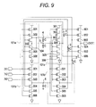
- FIG. 9 is a circuit diagram illustrating a configuration example of another latch circuit with three inputs and one output.
- the latch circuit in FIG. 9 is constituted by providing transistors 901 to 906 to the latch circuit in FIG. 8 instead of the transistors 801 and 802 . This latch circuit performs the same operation. A different point of the latch circuit in FIG. 9 from the latch circuit in FIG. 8 will be described below.
- a gate of the p-channel transistor 901 is connected to the node 1 , and a source thereof is connected to the power supply voltage node.
- a gate of the p-channel transistor 902 is connected to the node 2 , and a source thereof is connected to a drain of the p-channel transistor 901 .
- a gate of the p-channel transistor 903 is connected to the node 3 , a source thereof is connected to a drain of the p-channel transistor 902 , and a drain thereof is connected to the output terminal OUT 1 .
- a gate of the n-channel transistor 904 is connected to the node 3 , and a drain thereof is connected to the output terminal OUT 1 .
- a gate of the n-channel transistor 905 is connected to the node 2 , and a drain thereof is connected to a source of the n-channel transistor 904 .
- a gate of the n-channel transistor 906 is connected to the node 1 , a drain thereof is connected to a source of the n-channel transistor 905 , and a source thereof is connected to the reference potential node.
- FIG. 10 is a circuit diagram illustrating a configuration example of a latch circuit with a data terminal and a clock terminal.
- the latch circuit in FIG. is constituted by adding a data terminal DT, a clock terminal CK, transistors 1001 n , 1001 p , 1002 n , 1002 p , 1003 n and 1003 p , and an inverter 1004 to the latch circuit in FIG. 9 .
- the data terminal DT is for inputting data
- the clock terminal CK is for inputting a clock signal.
- the inverter 1004 inverts the clock signal of the clock terminal CK so as to output it.
- a gate of the n-channel transistor 1001 n is connected to the clock terminal K, a source and a drain thereof are connected to the data terminal DT and the node 1 , respectively.
- a gate of the p-channel transistor 1001 p is connected to an output terminal of the inverter 1004 , and a source and a drain thereof are connected to the data terminal DT and the node 1 , respectively.
- a gate of the n-channel transistor 1002 n is connected to the clock terminal CK, and a source and a drain thereof are connected to the data terminal DT and the node 2 , respectively.
- a gate of the p-channel transistor 1002 p is connected to the output terminal of the inverter 1004 , and a source and a drain thereof are connected to the data terminal DT and the node 2 , respectively.
- a gate of the n-channel transistor 1003 n is connected to the clock terminal CK, and a source and a drain thereof are connected to the data terminal DT and the node 3 , respectively.
- a gate of the p-channel transistor 1003 p is connected to the output terminal of the inverter 1004 , and a source and a drain thereof are connected to the data terminal DT and the node 3 .
- the transistors 1001 n , 1001 p , 1002 n , 1002 p , 1003 n and 1003 p are turned off, and the data terminal DT is disconnected from the nodes 1 to 3 .
- the nodes 1 to 3 retain previous data. This state is a data retaining mode.
- the same data of the data terminal DT are written into the nodes 1 to 3 .
- the output terminal OUT 1 outputs inverted data of the data of the data terminal DT.
- the output terminals OUTA and OUTB retain previous data, thereby preventing the soft error. Even when the two or less of the three nodes 4 to 6 invert data simultaneously due to soft error, the output terminals OUTA and OUTB retain previous data, thereby preventing the soft error.
- FIG. 11 is a circuit diagram illustrating a configuration example of another latch circuit having a data terminal and a clock terminal.
- the latch circuit in FIG. 11 is constituted by providing transistors 1101 n , 1101 p , 1102 n , 1102 p , 1103 n and 1103 p to the latch circuit in FIG. 10 instead of the transistors 1001 n , 1001 p , 1002 n , 1002 p , 1003 n and 1003 p .
- the circuit in FIG. 11 performs a similar operation. The different points of the latch circuit in FIG. 11 from the latch circuit in FIG. 10 will be described below.
- a gate of the n-channel transistor 1103 n is connected to the clock terminal CK, and a source and a drain thereof are connected to the data terminal DT and the node 1 , respectively.
- a gate of the p-channel transistor 1103 p is connected to the output terminal of the inverter 1004 , and a source and a drain thereof are connected to the data terminal DT and the node 1 , respectively.
- a gate of the n-channel transistor 1102 n is connected to the clock terminal CK, and a source and a drain thereof are connected to the node 1 and the node 2 , respectively.
- a gate of the p-channel transistor 1102 p is connected to the output terminal of the inverter 1004 , and a source and a drain thereof are connected to the node 1 and the node 2 respectively.
- a gate of the n-channel transistor 1101 n is connected to the clock terminal CK, and a source and a drain thereof are connected to the node 2 and the node 3 , respectively.
- a gate of the p-channel transistor 1101 p is connected to the output terminal of the inverter 1004 , and a source and a drain thereof are connected to the node 2 and the node 3 , respectively.
- the transistors 1101 n , 1101 p , 1102 n , 1102 p , 1103 n and 1103 p are turned off, and the data terminal DT is disconnected from the nodes 1 to 3 .
- the nodes 1 to 3 retain previous data.
- FIG. 7 is a diagram illustrating a configuration example of the latch circuit according to aspects of a second exemplary variation of the present invention.
- the different points of the latch circuit in FIG. 7 from the latch circuit in FIG. 1 will be described below.
- the latch circuit 205 has the four data inverting gates 101 a , 101 b , 101 c and 101 d .
- Three input terminals of the data inverting gate 101 a are connected to the node, 1 , the node 2 and the node 3 , and two output terminals thereof are connected to an input terminal of an inverter 701 and the node 4 .
- the inverter 701 inverts input data from the input terminal so as to output it from an output terminal.
- the output terminal of the inverter 701 is connected to the node 3 .
- the input terminal of the inverter 701 , the node 3 and the node 4 are connected to the capacitor C.
- Three input terminals of the data inverting gate 101 b are connected to the node 1 , the node 2 and the node 3 , and one output terminal thereof is connected to the node 5 .
- the node 5 is connected to the capacitor C.
- Three input terminals of the data inverting gate 101 c are connected to the node 4 , the node 5 and the node 6 , and one output terminal thereof is connected to the node 1 .
- the node 1 is connected to the capacitor C.
- Three input terminals of the data inverting gate 101 d are connected to the node 4 , the node 5 and the node 6 , and two output terminals thereof are connected to an input terminal of the inverter 702 and the node 2 .
- the inverter 702 inverts the input data from the input terminal so as to output it from an output terminal.
- the output terminal of the inverter 702 is connected to the node 6 .
- the input terminal of the inverter 702 , the node 2 and the node 6 are connected to the capacitor C.
- the nodes having the same numbers are connected to each other.
- the output terminal of the data inverting gate 101 c is connected to the input terminals of the two data inverting gates 101 a and 101 b via the node 1 .
- the two output terminals of the data inverting gate 101 d are connected to the input terminals of the two data inverting gates 101 a and 101 b via the node 2 .
- the output terminal of the inverter 701 is connected to the input terminals of the two data inverting gates 101 a and 101 b via the node 3 .
- the output terminal of the data inverting gate 101 a is connected to the input terminals of the two data inverting gates 101 c and 101 d via the node 4 .
- the output terminal of the data inverting gate 101 b is connected to the input terminals of the two data inverting gates 101 c and 101 d via the node 5 .
- the output terminal of the inverter 702 is connected to the input terminals of the two data inverting gates 101 c and 101 d via the node 6 .
- the configurations of the data inverting gates 10 . a to 101 d are the same as those in the first exemplary variation. Similarly to the first variation, as shown in the truth tables in FIGS. 4 and 5 , even when the data inverting gates 101 a to 101 d invert two or less data in the input data from the three input terminals INA to INC due to soft error, the output terminals OUTA and OUTB retain previous data. As a result, the soft error can be prevented.
- FIGS. 12A to 12C are diagrams illustrating configurations exemplary of the latch circuit according to aspects of a third exemplary variation of the present invention. The different points of the third variation from the first variation will be described below.
- the latch circuit 205 has five data inverting gates 101 a , 101 b , 101 c , 101 d and 101 e .
- Three input terminals of the data inverting gate 101 a are connected to the node 1 , the node 2 and the node 3 , and two output terminals thereof are connected to the node 4 and the node 5 .
- the output node 4 and the output node 5 are connected to the capacitor C.
- Three input terminals of the data inverting gate 101 b are connected to the node 1 , the node 2 and the node 3 , and two output terminals thereof are connected to the node 6 and a node 7 .
- the output node 6 and the output node 7 are connected to the capacitor C.
- Three input terminals of the data inverting gate 101 c are connected to the node 4 , the node 5 and the node 6 , and one output terminal thereof is connected to the node 1 .
- the output node 1 is connected to the capacitor C.
- Three input terminals of the data inverting gate 101 d are connected to the node 6 , the node 7 and the node 4 , and one output terminal thereof is connected to the node 2 .
- the output node 2 is connected to the capacitor C.
- Three input terminals of the data inverting gate 101 e are connected to the node 7 , the node 4 and the node 5 , and one output terminal thereof is connected to the node 3 .
- the output node 3 is connected to the capacitor C.
- the nodes having the same numbers are connected to each other.
- the data inverting gates 101 a and 101 b with three inputs and two outputs have the circuit configurations shown in FIGS. 3B to 3D .
- the data inverting gates 101 c , 101 . d and 101 e with three inputs and one output have the circuit configuration shown in FIG. 3A .
- the same data is input from outside into the nodes 1 to 3 .
- the latch circuit 205 in FIG. 12B will be described below.
- the latch circuit 205 has the four data inverting gates 101 a , 101 b , 101 c and 101 d .
- the three input terminals of the data inverting gate 101 a are connected to the node 1 , the node 2 and the node 3 , and the two output terminals thereof are connected to the node 5 and the node 6 .
- the output node 5 and the output node 6 are connected to the capacitor C.
- the three input terminals of the data inverting gate 101 b are connected to the node 1 , the node 2 and the node 4 , and the two output terminals thereof are connected to the node 7 and a node 8 .
- the output node 7 and the output node 8 are connected to the capacitor C.
- the three input terminals of the data inverting gate 101 c are connected to the node 5 , the node 6 and the node 7 , and the two output terminals thereof are connected to the node and the node 2 .
- the output node 1 and the output node 2 are connected to the capacitor C.
- the three input terminals of the data inverting gate 101 d are connected to the node 7 , the node 8 and the node 5 , and the two output terminals thereof are connected to the node 3 and the node 4 .
- the output node 3 and the output node 4 are connected to the capacitor C.
- the nodes having the same numbers are connected to each other.
- the data inverting gates 101 a to 101 d with three inputs and two outputs have the circuit configurations shown in FIGS. 3B to 3D . The same data is input from outside into the nodes 1 to 4 .
- the latch circuit 205 has four data inverting gates 101 a , 101 b , 101 c and 101 d .
- the three input terminals of the data inverting gate 101 a are connected to the node 1 , the node 2 and the node 3 , and the two output terminals thereof are connected to the node 5 and the node 6 .
- the output node 5 and the output node 6 are connected to the capacitor C.
- the three input terminals of the data inverting gate 101 b are connected to the node 1 , the node 2 and the node 4 , and the one output terminal thereof is connected to the node 7 .
- the output node 7 is connected to the capacitor C.
- the three input terminals of the data inverting gate 101 c are connected to the node 5 , the node 6 and the node 7 , and the two output terminals thereof are connected to the node 1 and the node 2 .
- the output node 1 and the output node 2 are connected to the capacitor C.
- the three input terminals of the data inverting gate 101 d are connected to the node 5 , the node 6 and the node 7 , and the two output terminals thereof are connected to the node 3 and the node 4 .
- the output node 3 and the output node 4 are connected to the capacitor C.
- the nodes having the same numbers are connected to each other.
- the data inverting gates 101 a , 101 c and 101 d with three inputs and two outputs have the circuit configurations shown in FIGS. 3 B to 3 D.
- the data inverting gate 101 b with three inputs and one output has the circuit configuration shown in FIG. 3A .
- the same data are input from outside into the nodes 1 to 4 .
- the same data at the data terminal DT is written into the plurality of input terminals of the respective data inverting gates.
- the data inverting gates output inverted data of the input data as described above.
- the data inverting gate When attention is paid to one data inverting gate, the data inverting gate has three input terminals INA to INC. Even when an error signal is input into two of the input terminals INA to INC, as shown in FIGS. 4 and 5 , the output terminals OUTA and OUTB are not influenced by the error signal. Therefore, as shown in FIG. 6 , the data inverting gates are connected, so that even if an error occurs on any two nodes, the data inverting gates can prevent noise due to the error. Therefore, the latch circuit is strongly resistant to soft error, and thus electronic devices having such a latch circuit are very resistance to soft error.
- the area of a parity arithmetic circuit does not need to be increased, thereby preventing a reduction in speed of the parity arithmetic that would be caused by such an increase.
- the latch circuit and the electronic devices having the latch circuit in the above exemplary variations can maintain an ideal speed, prevent soft errors, and improve reliability.
- the capacitor C may be parasitic capacitor, and may be, for example, wiring capacitor and/or gate capacitor of transistors.
- the latch circuit in the first to third exemplary variations has four or more gates.
- a generic term for data inverting gates 101 a to 101 e is data inverting gate 101 .
- the four or more gates are the data inverting gate 101 or the inverters 701 and 702 .
- At least one of the four or more gates has three input terminals INA to INC and one or two output terminals OUTA and OUTB. When all the data to be input into the three input terminals is the same, inverted data is output from the output terminals. When all the data to be input into the three input terminals is not the same, the data inverting gate 101 retains previous data.
- the four or more gates constitute a feedback circuit.
- the capacitor C is a data retaining section which is connected to the output terminal of the data inverting gate 101 and retains data at the output terminal.
- the data inverting gate 101 brings at least one output terminal into a high-impedance state and retains previous data retained in the data retaining section C.
- At least four of the four or more gates are the data inverting gate 101 .
- one of the at least four data inverting gates has three input terminals and two output terminals, and another one of the at least four data inverting gates has three input terminals and one output terminal.
- the at least four data inverting gates have three input terminals and two output terminals.
- the respective data inverting gates 101 have three or more field-effect transistors whose gates are connected to the three input terminals INA to INC and which are connected to each other in series.
- the data inverting gates 101 have the three p-channel field-effect transistors 301 to 303 and the three n-channel field-effect transistors 304 to 306 whose gates are connected to the three input terminals INA to INC and which are connected to each other in series.
- the three p-channel field-effect transistors 301 to 303 are first to third p-channel field-effect transistors, and the three n-channel field-effect transistors 304 to 306 are first to third n-channel field-effect transistors.
- the data inverting gate 101 has one output terminal OUTA, and the one output terminal OUTA is connected to an interconnecting point between the drain of the third p-channel field-effect transistor 303 and the drain of the first n-channel field-effect transistor 304 .
- the three p-channel field-effect transistors 301 to 303 are first to third p-channel field-effect transistors
- the three n-channel field-effect transistors 304 to 306 are first to third n-channel field-effect transistors.
- the data inverting gate 101 has the first and second output terminals OUTA and OUTB, and the first output terminal OUTA is connected to an interconnecting point between the second and third p-channel field-effect transistors 302 and 303 , and to an interconnecting point between the first and second n-channel field-effect transistors 304 and 305 .
- the second output terminal OUTB is connected to an interconnecting point between the drain of the third p-channel field-effect transistor 303 and the drain of the first n-channel field-effect transistor 304 .
- the same data of the data terminal DT is input into the three input terminals INA to INC of the data inverting gate 101 from the outside.
- the transistors 1001 n , 1001 p , 1002 n , 1002 p , 1003 n , 1003 p , 1101 n , 1101 p , 1102 n , 1102 p , 1103 n and 1103 p are switches for inputting the same data of the data terminal DT into the three input terminals INA to INC of the data inverting gate 101 according to a clock signal of the clock terminal CK.
- the transistors 801 , 802 and 901 to 906 are a plurality of output field-effect transistors whose gates are connected to output terminals of two of the four or more gates, and which are connected to each other in series and output data.
- the data inverting gate Since the data inverting gate has three input terminals, even if data is inverted at one or two of the three input terminals due to soft error, the data inverting gate can retain previous data. As a result, the data inverting gate as the latch circuit can prevent the soft error, so that reliability can be improved. Since a parity arithmetic circuit is not necessary for preventing soft error, the area of the parity arithmetic circuit does not need to be increased, so that a reduction in speed due to the parity arithmetic can be prevented.
Landscapes
- Logic Circuits (AREA)
Abstract
Description
Claims (14)
Applications Claiming Priority (2)
| Application Number | Priority Date | Filing Date | Title |
|---|---|---|---|
| JP2008-079832 | 2008-03-26 | ||
| JP2008079832A JP4968130B2 (en) | 2008-03-26 | 2008-03-26 | Latch circuit and electronic device |
Publications (2)
| Publication Number | Publication Date |
|---|---|
| US20090243686A1 US20090243686A1 (en) | 2009-10-01 |
| US8072251B2 true US8072251B2 (en) | 2011-12-06 |
Family
ID=41116174
Family Applications (1)
| Application Number | Title | Priority Date | Filing Date |
|---|---|---|---|
| US12/388,689 Expired - Fee Related US8072251B2 (en) | 2008-03-26 | 2009-02-19 | Latch circuit and electronic device |
Country Status (2)
| Country | Link |
|---|---|
| US (1) | US8072251B2 (en) |
| JP (1) | JP4968130B2 (en) |
Families Citing this family (2)
| Publication number | Priority date | Publication date | Assignee | Title |
|---|---|---|---|---|
| JP6703249B2 (en) * | 2015-05-27 | 2020-06-03 | 国立大学法人東北大学 | Storage device |
| JP7283697B2 (en) * | 2017-06-12 | 2023-05-30 | 国立研究開発法人宇宙航空研究開発機構 | Single-event upset-tolerant latch and flip-flop circuits |
Citations (3)
| Publication number | Priority date | Publication date | Assignee | Title |
|---|---|---|---|---|
| JP2007248378A (en) | 2006-03-17 | 2007-09-27 | Fujitsu Ltd | Semiconductor integrated circuit |
| US20070268055A1 (en) * | 2006-05-18 | 2007-11-22 | William Yeh-Yung Mo | Radiation Hardened Programmable Phase Frequency Divider for Deep Submicron CMOS Technology |
| US20070268054A1 (en) | 2006-05-18 | 2007-11-22 | Fujitsu Limited | Latch circuit |
Family Cites Families (8)
| Publication number | Priority date | Publication date | Assignee | Title |
|---|---|---|---|---|
| JPS61294931A (en) * | 1985-06-21 | 1986-12-25 | Mitsubishi Electric Corp | Semiconductor device and data transmission line |
| JPS61294932A (en) * | 1985-06-21 | 1986-12-25 | Mitsubishi Electric Corp | Semiconductor device and data transmission line |
| JP2003173681A (en) * | 2001-12-07 | 2003-06-20 | Mitsubishi Electric Corp | Semiconductor memory circuit and latch circuit |
| JP3718687B2 (en) * | 2002-07-09 | 2005-11-24 | 独立行政法人 宇宙航空研究開発機構 | Inverter, semiconductor logic circuit, static random access memory, and data latch circuit |
| US6937527B1 (en) * | 2004-05-27 | 2005-08-30 | Hewlett-Packard Development Company, L.P. | High reliability triple redundant latch with voting logic on each storage node |
| US7068088B2 (en) * | 2004-10-27 | 2006-06-27 | Hewlett-Packard Development Company, L.P. | Soft-error rate improvement in a latch |
| US7236001B2 (en) * | 2005-09-02 | 2007-06-26 | Honeywell International Inc. | Redundancy circuits hardened against single event upsets |
| JP4873459B2 (en) * | 2006-05-22 | 2012-02-08 | ルネサスエレクトロニクス株式会社 | Latch circuit and semiconductor integrated circuit |
-
2008
- 2008-03-26 JP JP2008079832A patent/JP4968130B2/en not_active Expired - Fee Related
-
2009
- 2009-02-19 US US12/388,689 patent/US8072251B2/en not_active Expired - Fee Related
Patent Citations (6)
| Publication number | Priority date | Publication date | Assignee | Title |
|---|---|---|---|---|
| JP2007248378A (en) | 2006-03-17 | 2007-09-27 | Fujitsu Ltd | Semiconductor integrated circuit |
| US20070226600A1 (en) | 2006-03-17 | 2007-09-27 | Fujitsu Limited | Semiconductor integrated circuit with flip-flops having increased reliability |
| US20070268055A1 (en) * | 2006-05-18 | 2007-11-22 | William Yeh-Yung Mo | Radiation Hardened Programmable Phase Frequency Divider for Deep Submicron CMOS Technology |
| US20070268054A1 (en) | 2006-05-18 | 2007-11-22 | Fujitsu Limited | Latch circuit |
| JP2007312104A (en) | 2006-05-18 | 2007-11-29 | Fujitsu Ltd | Latch circuit |
| US20090140764A1 (en) * | 2006-05-18 | 2009-06-04 | Fujitsu Limited | Latch Circuit |
Also Published As
| Publication number | Publication date |
|---|---|
| JP4968130B2 (en) | 2012-07-04 |
| JP2009239405A (en) | 2009-10-15 |
| US20090243686A1 (en) | 2009-10-01 |
Similar Documents
| Publication | Publication Date | Title |
|---|---|---|
| US7759995B2 (en) | Semiconductor integrated circuit with a logic circuit including a data holding circuit | |
| US6327176B1 (en) | Single event upset (SEU) hardened latch circuit | |
| US8035410B2 (en) | Latch circuit | |
| US20040007743A1 (en) | Inverter, semiconductor logic circuit, static random access memory and data latch circuit | |
| US7649396B2 (en) | Soft error rate hardened latch | |
| US8723548B2 (en) | Hysteresis-based latch design for improved soft error rate with low area/performance overhead | |
| KR100991386B1 (en) | Exclusive or logic circuit | |
| US6975151B2 (en) | Latch circuit having reduced input/output load memory and semiconductor chip | |
| US8072251B2 (en) | Latch circuit and electronic device | |
| US8513999B2 (en) | Semiconductor device | |
| US7411411B1 (en) | Methods and systems for hardening a clocked latch against single event effects | |
| US9165917B2 (en) | In-line stacking of transistors for soft error rate hardening | |
| US7242219B1 (en) | Circuit for parity tree structure | |
| US7289375B2 (en) | Data holding circuit | |
| US20060279347A1 (en) | Semiconductor integrated circuit | |
| US7719337B2 (en) | Semiconductor device | |
| Musala et al. | Self testing and fault secure XOR/XNOR circuit using FinFETs | |
| US8421503B2 (en) | Latch circuit | |
| JP4587788B2 (en) | Logic circuit | |
| US20220209752A1 (en) | Semiconductor device | |
| US9997210B2 (en) | Data register for radiation hard applications | |
| US20260081585A1 (en) | Robust single event upset (seu) tolerant high-performance flip-flop | |
| US20050264334A1 (en) | Semiconductor integrated circuit using latch circuit with noise tolerance | |
| KR20160020790A (en) | Semiconductor device | |
| US20150171840A1 (en) | Latch circuit and semiconductor integrated circuit |
Legal Events
| Date | Code | Title | Description |
|---|---|---|---|
| AS | Assignment |
Owner name: FUJITSU MICROELECTRONICS LIMITED, JAPAN Free format text: ASSIGNMENT OF ASSIGNORS INTEREST;ASSIGNORS:UEMURA, TAIKI;TOSAKA, YOSHIHARU;REEL/FRAME:022285/0177 Effective date: 20090121 |
|
| AS | Assignment |
Owner name: FUJITSU SEMICONDUCTOR LIMITED, JAPAN Free format text: CHANGE OF NAME;ASSIGNOR:FUJITSU MICROELECTRONICS LIMITED;REEL/FRAME:024748/0328 Effective date: 20100401 |
|
| FEPP | Fee payment procedure |
Free format text: PAYOR NUMBER ASSIGNED (ORIGINAL EVENT CODE: ASPN); ENTITY STATUS OF PATENT OWNER: LARGE ENTITY |
|
| STCF | Information on status: patent grant |
Free format text: PATENTED CASE |
|
| AS | Assignment |
Owner name: SOCIONEXT INC., JAPAN Free format text: ASSIGNMENT OF ASSIGNORS INTEREST;ASSIGNOR:FUJITSU SEMICONDUCTOR LIMITED;REEL/FRAME:035508/0637 Effective date: 20150302 |
|
| FPAY | Fee payment |
Year of fee payment: 4 |
|
| FEPP | Fee payment procedure |
Free format text: MAINTENANCE FEE REMINDER MAILED (ORIGINAL EVENT CODE: REM.); ENTITY STATUS OF PATENT OWNER: LARGE ENTITY |
|
| LAPS | Lapse for failure to pay maintenance fees |
Free format text: PATENT EXPIRED FOR FAILURE TO PAY MAINTENANCE FEES (ORIGINAL EVENT CODE: EXP.); ENTITY STATUS OF PATENT OWNER: LARGE ENTITY |
|
| STCH | Information on status: patent discontinuation |
Free format text: PATENT EXPIRED DUE TO NONPAYMENT OF MAINTENANCE FEES UNDER 37 CFR 1.362 |
|
| FP | Lapsed due to failure to pay maintenance fee |
Effective date: 20191206 |