US8071894B2 - Semiconductor device having a mount board - Google Patents
Semiconductor device having a mount board Download PDFInfo
- Publication number
- US8071894B2 US8071894B2 US11/984,176 US98417607A US8071894B2 US 8071894 B2 US8071894 B2 US 8071894B2 US 98417607 A US98417607 A US 98417607A US 8071894 B2 US8071894 B2 US 8071894B2
- Authority
- US
- United States
- Prior art keywords
- socket
- heat radiation
- semiconductor device
- board
- mount board
- Prior art date
- Legal status (The legal status is an assumption and is not a legal conclusion. Google has not performed a legal analysis and makes no representation as to the accuracy of the status listed.)
- Expired - Fee Related, expires
Links
Images


Classifications
-
- G—PHYSICS
- G06—COMPUTING; CALCULATING OR COUNTING
- G06F—ELECTRIC DIGITAL DATA PROCESSING
- G06F1/00—Details not covered by groups G06F3/00 - G06F13/00 and G06F21/00
- G06F1/16—Constructional details or arrangements
- G06F1/18—Packaging or power distribution
- G06F1/183—Internal mounting support structures, e.g. for printed circuit boards, internal connecting means
- G06F1/185—Mounting of expansion boards
-
- G—PHYSICS
- G06—COMPUTING; CALCULATING OR COUNTING
- G06F—ELECTRIC DIGITAL DATA PROCESSING
- G06F1/00—Details not covered by groups G06F3/00 - G06F13/00 and G06F21/00
- G06F1/16—Constructional details or arrangements
- G06F1/20—Cooling means
-
- H—ELECTRICITY
- H01—ELECTRIC ELEMENTS
- H01L—SEMICONDUCTOR DEVICES NOT COVERED BY CLASS H10
- H01L23/00—Details of semiconductor or other solid state devices
- H01L23/34—Arrangements for cooling, heating, ventilating or temperature compensation ; Temperature sensing arrangements
- H01L23/36—Selection of materials, or shaping, to facilitate cooling or heating, e.g. heatsinks
- H01L23/373—Cooling facilitated by selection of materials for the device or materials for thermal expansion adaptation, e.g. carbon
- H01L23/3735—Laminates or multilayers, e.g. direct bond copper ceramic substrates
-
- H—ELECTRICITY
- H01—ELECTRIC ELEMENTS
- H01L—SEMICONDUCTOR DEVICES NOT COVERED BY CLASS H10
- H01L23/00—Details of semiconductor or other solid state devices
- H01L23/34—Arrangements for cooling, heating, ventilating or temperature compensation ; Temperature sensing arrangements
- H01L23/46—Arrangements for cooling, heating, ventilating or temperature compensation ; Temperature sensing arrangements involving the transfer of heat by flowing fluids
- H01L23/467—Arrangements for cooling, heating, ventilating or temperature compensation ; Temperature sensing arrangements involving the transfer of heat by flowing fluids by flowing gases, e.g. air
-
- H—ELECTRICITY
- H05—ELECTRIC TECHNIQUES NOT OTHERWISE PROVIDED FOR
- H05K—PRINTED CIRCUITS; CASINGS OR CONSTRUCTIONAL DETAILS OF ELECTRIC APPARATUS; MANUFACTURE OF ASSEMBLAGES OF ELECTRICAL COMPONENTS
- H05K1/00—Printed circuits
- H05K1/02—Details
- H05K1/0201—Thermal arrangements, e.g. for cooling, heating or preventing overheating
- H05K1/0203—Cooling of mounted components
- H05K1/0209—External configuration of printed circuit board adapted for heat dissipation, e.g. lay-out of conductors, coatings
-
- H—ELECTRICITY
- H05—ELECTRIC TECHNIQUES NOT OTHERWISE PROVIDED FOR
- H05K—PRINTED CIRCUITS; CASINGS OR CONSTRUCTIONAL DETAILS OF ELECTRIC APPARATUS; MANUFACTURE OF ASSEMBLAGES OF ELECTRICAL COMPONENTS
- H05K7/00—Constructional details common to different types of electric apparatus
- H05K7/20—Modifications to facilitate cooling, ventilating, or heating
- H05K7/2039—Modifications to facilitate cooling, ventilating, or heating characterised by the heat transfer by conduction from the heat generating element to a dissipating body
- H05K7/205—Heat-dissipating body thermally connected to heat generating element via thermal paths through printed circuit board [PCB]
-
- H—ELECTRICITY
- H01—ELECTRIC ELEMENTS
- H01L—SEMICONDUCTOR DEVICES NOT COVERED BY CLASS H10
- H01L2924/00—Indexing scheme for arrangements or methods for connecting or disconnecting semiconductor or solid-state bodies as covered by H01L24/00
- H01L2924/0001—Technical content checked by a classifier
- H01L2924/0002—Not covered by any one of groups H01L24/00, H01L24/00 and H01L2224/00
-
- H—ELECTRICITY
- H05—ELECTRIC TECHNIQUES NOT OTHERWISE PROVIDED FOR
- H05K—PRINTED CIRCUITS; CASINGS OR CONSTRUCTIONAL DETAILS OF ELECTRIC APPARATUS; MANUFACTURE OF ASSEMBLAGES OF ELECTRICAL COMPONENTS
- H05K1/00—Printed circuits
- H05K1/02—Details
- H05K1/14—Structural association of two or more printed circuits
-
- H—ELECTRICITY
- H05—ELECTRIC TECHNIQUES NOT OTHERWISE PROVIDED FOR
- H05K—PRINTED CIRCUITS; CASINGS OR CONSTRUCTIONAL DETAILS OF ELECTRIC APPARATUS; MANUFACTURE OF ASSEMBLAGES OF ELECTRICAL COMPONENTS
- H05K2201/00—Indexing scheme relating to printed circuits covered by H05K1/00
- H05K2201/04—Assemblies of printed circuits
- H05K2201/044—Details of backplane or midplane for mounting orthogonal PCBs
-
- H—ELECTRICITY
- H05—ELECTRIC TECHNIQUES NOT OTHERWISE PROVIDED FOR
- H05K—PRINTED CIRCUITS; CASINGS OR CONSTRUCTIONAL DETAILS OF ELECTRIC APPARATUS; MANUFACTURE OF ASSEMBLAGES OF ELECTRICAL COMPONENTS
- H05K2201/00—Indexing scheme relating to printed circuits covered by H05K1/00
- H05K2201/06—Thermal details
- H05K2201/066—Heatsink mounted on the surface of the PCB
-
- H—ELECTRICITY
- H05—ELECTRIC TECHNIQUES NOT OTHERWISE PROVIDED FOR
- H05K—PRINTED CIRCUITS; CASINGS OR CONSTRUCTIONAL DETAILS OF ELECTRIC APPARATUS; MANUFACTURE OF ASSEMBLAGES OF ELECTRICAL COMPONENTS
- H05K2201/00—Indexing scheme relating to printed circuits covered by H05K1/00
- H05K2201/09—Shape and layout
- H05K2201/09209—Shape and layout details of conductors
- H05K2201/09654—Shape and layout details of conductors covering at least two types of conductors provided for in H05K2201/09218 - H05K2201/095
- H05K2201/09781—Dummy conductors, i.e. not used for normal transport of current; Dummy electrodes of components
-
- H—ELECTRICITY
- H05—ELECTRIC TECHNIQUES NOT OTHERWISE PROVIDED FOR
- H05K—PRINTED CIRCUITS; CASINGS OR CONSTRUCTIONAL DETAILS OF ELECTRIC APPARATUS; MANUFACTURE OF ASSEMBLAGES OF ELECTRICAL COMPONENTS
- H05K2201/00—Indexing scheme relating to printed circuits covered by H05K1/00
- H05K2201/10—Details of components or other objects attached to or integrated in a printed circuit board
- H05K2201/10007—Types of components
- H05K2201/10189—Non-printed connector
Definitions
- the present invention relates to a semiconductor device having a mount board in which a module board provided with one or a plurality of electronic components is mounted on a socket and, more particularly, to a technique of cooling the module board mounted on the mount board.
- a conventional memory device such as a DRAM (Dynamic Random Access Memory) device is directly mounted on a motherboard (mount board).
- a memory module board on which one or a plurality of memory devices are mounted on a printed circuit board is prepared separately from a mount board, and is mounted on the mount board by a socket provided on the surface of the mount board.
- the amount of heat generated in the memory devices increases in accordance with the development of a higher density of memory devices mounted and increase in the read/write speed thereof.
- the increase in the amount of heat generated in a memory device has involved an excessive temperature rise in the memory module board. This causes a problem of operation errors and system down in the electronic devices.
- Patent Publications JP-A-2004-079940 (FIG. 2), JP-A-2003-017634 (FIG. 1), and JP-A-2001-118984 (FIG. 1) describe that various heat radiation members are provided on the side surfaces of a memory module board, on which memory devices are provided, to radiate heat from the side surfaces of the memory module board, thereby suppressing the temperature rise thereof.
- the present invention provides, in a first aspect thereof, a semiconductor device including: a module board mounting thereon an electric component and having a plug at an edge of the module board; and a mount board having thereon a socket adapted to the plug on a surface portion of the mount board, for mounting thereon the module board via the plug,
- the socket includes a heat radiation guide plate in contact with a side surface of the socket.
- the present invention provides, in a second aspect thereof, a semiconductor device including: a module board mounting thereon an electric component and having a plug at an edge of the module board; and a mount board having thereon a socket adapted to the plug on a surface portion of the mount board for mounting thereon the module board via the plug,
- the surface portion of the mount board has a thermal conductivity of 1 watt/meter ⁇ K or above.
- the semiconductor device of the first aspect of the present invention most of heat generated from the module board is radiated from the socket through the heat radiation guide plate in addition to conventional heat radiation paths, when the semiconductor device is supplied with electric power and the module board is operating. Therefore, in comparison with the conventional semiconductor devices, the heat generated in the module board is efficiently radiated therefrom, and temperature rise of the module board can be effectively suppressed.
- heat transferred to the surface portion of the mount board that the socket contacts quickly spreads in the in-plane directions of the mount board and is radiated to the mount board having a large heat capacity, when the semiconductor device is supplied with electric power and the module board is operating.
- the surface portion of the mount board has a high thermal conductivity. Therefore, in comparison with the conventional semiconductor devices, the heat generated in the module board is efficiently radiated therefrom, and temperature rise of the module board can be effectively suppressed.
- the present invention can be applied to a semiconductor device in which the electronic component is a memory device. Thermal runaway caused by an excessive tem rise in the memory device can thereby be prevented.
- the heat radiation guide plates or the surface portion, on which the memory module is mounted preferably have a thermal conductivity of 50 W/m ⁇ K or higher.
- iron, aluminum, copper or PGS can be used as the material having the thermal conductivity of 50 W/m ⁇ K or higher.
- FIG. 1 is a perspective view showing the structure of a semiconductor device according to a first embodiment of the present invention
- FIG. 2 is a top plan view showing the semiconductor device in FIG. 1 from which memory module boards are removed;
- FIGS. 3A and 3B are sectional views taken along the lines a-a and b-b in FIG. 1 ;
- FIG. 4A is a perspective view showing the structure of a semiconductor device according to a first modification of the first embodiment, and FIG. 4B is a sectional view taken along the line b-b in FIG. 4A ;
- FIG. 5 is a top plan view showing the structure of a semiconductor device according to a second modification of the first embodiment
- FIG. 6 is a top plan view showing the structure of a semiconductor device according to a third modification of the first embodiment
- FIG. 7 is a top plan view showing the structure of a semiconductor device according to a fourth modification of the first embodiment
- FIGS. 8A and 8B are sectional views showing a semiconductor device according to a second embodiment of the present invention, corresponding to FIGS. 3A and 3B ;
- FIG. 9 is a sectional view showing the structure of a semiconductor device according to a modification example of the second embodiment.
- the present inventor carried out a simulation, in which the thermal conduction paths are examined in a memory module board by thermal analysis, in order to find the structure for suppressing the temperature rise of a memory module board.
- the heat generated in the memory module board was radiated from the surface of the memory module board to the ambient air and simultaneously radiated through a socket toward the mount board.
- the amount of heat reached to the mount board was equal to about 45% of the whole heat radiation.
- the present inventor derived an idea that the temperature rise of the memory module board can be effectively suppressed by efficiently radiating the heat toward the mount board from the memory module board.
- the present inventor further discussed specifically the structure to efficiently radiate the heat from the memory module board to the mount board, and decided to provide a heat radiation guide plate which contacts each of the socket and the mount board.
- the memory module board is mounted on the socket via a plug.
- heat generated by the memory module board is transferred to the heat radiation guide plate from the combination of plug and socket, and further to the mount board therefrom.
- the heat is efficiently radiated from the memory module board.
- radiation of heat from the socket to the mount board was efficiently carried out by setting thermal conductivity of the heat radiation guide plate at higher than 1 W/m ⁇ K.
- the surface portion of the mount board that the socket or heat radiation guide plate contacts is configured by a heat radiation layer having a thermal conductivity of 1 W/m ⁇ K or higher, in place of the conventional layer having a thermal conductivity of less than 1 W/m ⁇ K.
- the heat transferred to the mount board through the combination of plug and socket or the heat radiation guide plate spreads quickly in the in-plane directions of the mount board through the heat radiation layer, and is radiated to the mount board having a larger thermal capacity through the heat radiation layer.
- the heat generated in the memory module board can be efficiently radiated to the mount board.
- a similar advantage can be obtained by providing a heat radiation sheet having a thermal conductivity of 1 W/m ⁇ K or higher on the mount board, which is kept in contact with the socket or heat radiation guide plate.
- the heat can be radiated more efficiently from the memory module if the heat radiation guide plate, heat radiation layer, or heat radiation sheet is made of iron, aluminum, copper or a material having a thermal conductivity of 50 W/m ⁇ K or higher, such as PGS.
- FIG. 1 is a perspective view showing the structure of a semiconductor device according to a first embodiment of the present invention.
- FIG. 2 is a top plan view showing the semiconductor device shown in FIG. 1 , from which memory module boards are removed.
- the semiconductor device generally designated by numeral 100 , has a mount board 10 , an elongate socket 20 provided on the mount board 10 , and memory module boards 30 mounted on the socket 20 .
- the memory module board 30 is a card-like board having a rectangular shape.
- a plurality of memory devices 31 are provided on both surfaces of the memory module board 30 , and an elongate plug is provided on an edge portion of the memory module board 30 .
- the plug has a plurality of plug terminals arranged in a row on both sides of the memory module board 30 and near the edge of the memory module board 30 .
- the socket 20 has a plurality of socket terminals arranged in two rows and each corresponding to one of the plug terminals of the plug.
- the mount board 10 is configured as a multilayer printed circuit board, and has a structure in which a plurality of insulating layers 11 of FR4 (Flame Retardant Type 4) are layered one on another.
- the socket In an area underlying the socket 20 except for the center of the socket 20 , a heat radiation layer 13 made of copper is formed in place of the uppermost insulating layer 11 a .
- Copper heat radiation guide plates 40 a and 40 b are provided in contact with the surface of the heat radiation layer 13 and the side surfaces of the socket 20 .
- FR4 and copper have a heat conductivity of about 0.3 W/m ⁇ K and 385 W/m ⁇ K, respectively.
- FIG. 3A shows a part of a cross-section taken along the line a-a shown in FIG. 1 .
- interconnection patterns made of copper are formed between adjacent two insulating layers 11 and on top and bottom surfaces of the mount board 10 .
- a number of through-holes (not shown) each penetrating the mount board 10 and a number of via holes (not shown) each penetrating one or a plurality of insulating layers 11 are formed in the mount board 10 .
- Interconnection plugs are formed inside these through-holes and via holes, thereby connecting together different interconnection layers.
- the area underlying the center of the socket 20 configures an interconnection area 12 .
- a plurality of via holes each penetrating one or a plurality of insulating layers 11 including the uppermost insulating layer 11 a are formed.
- a plurality of electrodes provided at the bottom of the socket 20 and extending from the respective socket terminals are connected to the interconnection plugs formed inside the via holes and through-holes.
- the socket 20 has a U-shaped cross-section.
- a plurality of socket terminals 21 are provided on both inner side surfaces of the U-shaped socket 20 .
- a plurality of plug terminals (not shown) are formed on both side surfaces of the board at a lower portion thereof. These plug terminals are coupled to the socket terminals 21 of the socket by insertion of the plug into the socket 21 .
- the heat radiation guide plates 40 a and 40 b have a height substantially equal to the height of the socket 20 .
- a grease (not shown) is applied between side surfaces of the socket 20 and the heat radiation guide plates 40 a and 40 b , to tighten the contact between the side surfaces of the socket 20 and the heat radiation guide plates 40 a and 40 b .
- efficiency of thermal conduction between the socket 20 and the heat radiation guide plates 40 a and 40 b is improved.
- FIG. 3B shows a longitudinal-section taken along the direction b-b shown in FIG. 1 and FIG. 3A .
- the heat radiation guide plates 40 a and 40 b have substantially the same dimensions as the side surface of the socket 20 in the lengthwise direction and in the height direction.
- the heat radiation guide plates 40 a and 40 b are provided adjacent to the socket 20 .
- the heat radiation layer 13 has such a planar shape that is large enough to encompass the whole bottom surface of the socket 20 and the heat radiation guide plates 40 a and 40 b , and yet does not obstruct connection of the mount board 10 .
- the heat radiation layer 13 made of copper is formed around the interconnection area 12 prior to formation of the uppermost insulating layer 11 a , during the process for forming the mount board 10 .
- the socket 20 is provided on the mount board 10 .
- the heat radiation guide plates 40 a and 40 b each are formed so as to contact a side surface of the socket 20 and the upper surface of the heat radiation layer 13 .
- the heat radiation layer 13 is made of copper.
- the heat radiation layer 13 may be made of another material having a thermal conductivity of 1 W/m ⁇ K or higher.
- the heat radiation layer 13 may preferably be made of a PGS (Pyrolytic Graphite Sheet).
- the PGS has a thermal conductivity of 600 to 800 W/m ⁇ K or so in the direction in which the crystal surface thereof extends, and a thermal conductivity of 15 W/m ⁇ K or so in the thickness direction of the crystal surface. Therefore, if the heat radiation layer 13 is made of PGS, the heat can be efficiently radiated by arranging the crystal surface of the PGS in parallel with the extending direction of the heat radiation layer 13 .
- the heat radiation guide plates 40 a and 40 b are made of copper.
- the heat radiation guide plates 40 a and 40 b may be made of another material.
- the heat radiation guide plates 40 a and 40 b may be made of aluminum having a thermal conductivity of 201 W/m ⁇ K, iron having a thermal conductivity of 80 W/m ⁇ K.
- the heat radiation layer 13 or heat radiation guide plates 40 a and 40 b may be made of insulating material having a high thermal conductivity. Examples of the insulating material having a high thermal conductivity include silicon nitride, aluminum nitride, and the like.
- FIG. 4A is a perspective view showing the structure of a semiconductor device according to a first modification of the first embodiment.
- FIG. 4B shows a longitudinal-section taken along the line b-b shown in FIG. 4A .
- heat radiation fins 41 are provided on a line extending from the longitudinal direction of the socket 20 and on the surface of the heat radiation layer 13 . That is, the heat radiation fins 41 are additionally provided in the structure of the semiconductor device 100 shown in FIG. 1 .
- the heat radiation fins 41 provided on the heat radiation layer 13 , assist radiation of the heat generated in the heat radiation layer 13 for the mount board 10 toward the ambient air. Accordingly, in comparison with the semiconductor device 100 shown in FIG. 1 , the temperature rise of the memory module board 30 can be more effectively suppressed.
- a heat radiation fan may be additionally provided on the mount board 10 .
- FIGS. 5 to 7 show semiconductor devices in which the heat radiation layer 13 is provided apart from the socket 20 , according to second to fourth modifications of the first embodiment.
- the interconnection area 12 is provided to encompass the whole bottom surfaces of the socket 20 and the heat radiation guide plates 40 a and 40 b.
- a plurality of interconnection areas 12 are provided each to encompass the bottom surface of a corresponding socket 20 and a corresponding pair of heat radiation guide plates 40 a and 40 b .
- first heat radiation layers 13 a to 13 c are provided each between adjacent two of the socket 20
- second heat radiation layers 13 d and 13 e are respectively provided outside of the outermost socket 20
- third heat radiation layers 13 f and 13 g are provided in the vicinity of the edges of the socket 20 arranged therein.
- the interconnection areas 12 are provided in the space between the heat radiation layers 13 a to 13 g . This configuration provides a simpler structure for the interconnection circuit.
- the heat radiation layers 13 having a high thermal conductivity and provided near the socket 20 in the semiconductor devices 102 , 103 , and 104 shown in FIGS. 5 to 7 effectively radiate the heat generated in the mount board 10 near the socket 20 in the in-plane directions of the mount board 10 .
- the temperature rise of the memory module board 30 can be effectively suppressed.
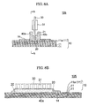
- FIGS. 8A and 8B show a cross-section and a longitudinal section, respectively, of a semiconductor device according to a second embodiment of the present invention.
- FIG. 8A shows the structure of the memory module similarly to FIG. 3A
- FIG. 8B shows the structure of the memory module similarly to FIG. 3B .
- the heat radiation layer 13 shown in FIG. 1 is not formed, and the uppermost insulating layer 11 a is formed over the entire surface of the mount board 10 .
- Heat radiation guide plates 40 a and 40 b are provided on the mount board 10 , which is in contact with the side surfaces of a socket 20 .
- Heat radiation sheets 14 are provided on the mount board 10 , which is in contact with the side surfaces of the heat radiation guide plates 40 a and 40 b .
- the semiconductor device 105 has a structure similar to the structure of the semiconductor device 100 shown in FIG. 1 except for the features described above.
- the heat radiation sheets 14 can be formed easily on the mount board 10 . Therefore, the semiconductor device 105 of the present embodiment can be more easily manufactured compared to the semiconductor device 100 of the first embodiment. In addition, the design choice of the circuit interconnections in the mount board 10 is increased since the heat radiation sheets 14 overlies an insulating layer 11 a .
- the heat radiation sheets 14 may be provided in contact with the side surfaces of the socket 20 , and heat radiation guide plates 40 a and 40 b may be provided on the heat radiation sheets 14 .
- FIG. 9 shows a longitudinal-section of the memory module board in a semiconductor device according to a modification of the second embodiment, similarly to FIG. 8B .
- the semiconductor device 106 of this modification corresponds to the structure of the semiconductor device 105 shown in FIG. 8 provided with heat radiation fins 41 on the surfaces of the heat radiation sheets 14 .
- the heat radiation fins 41 are arranged on the line extended from the extending direction of the socket 20 .
- the mount board 106 in the present modification the heat is effectively radiated from of the heat radiation sheets 14 or mount board 10 toward the ambient air through the fins 41 .
- a heat radiation fan may be provided on the mount board 10 .
- memory module boards have been described.
- temperature rise of a variety of module boards each provided with one or a plurality of other electronic components can be effectively suppressed by applying a structure similar to those described above.
- the temperature rise of the electronic component can be also effectively suppressed by forming a heat radiation layer as described above or by providing heat radiation guide plates and/or heat radiation sheets.
- the heat radiation guide plates are provided in contact with each of the electronic component and the mount board.
- the present invention has been described above based on preferred embodiments thereof.
- the semiconductor devices according to the present invention are not limited to the structures described in the embodiments.
- the scope of the present invention should be considered as including those semiconductor devices that would be derived by making various changes and modifications to the structures of the above embodiments.
Abstract
Description
Claims (23)
Priority Applications (1)
| Application Number | Priority Date | Filing Date | Title |
|---|---|---|---|
| US11/984,176 US8071894B2 (en) | 2005-02-09 | 2007-11-14 | Semiconductor device having a mount board |
Applications Claiming Priority (4)
| Application Number | Priority Date | Filing Date | Title |
|---|---|---|---|
| JP2005033011A JP2006221912A (en) | 2005-02-09 | 2005-02-09 | Semiconductor device |
| JP2005-033011 | 2005-02-09 | ||
| US11/349,200 US7307224B2 (en) | 2005-02-09 | 2006-02-08 | Semiconductor device having a mount board |
| US11/984,176 US8071894B2 (en) | 2005-02-09 | 2007-11-14 | Semiconductor device having a mount board |
Related Parent Applications (1)
| Application Number | Title | Priority Date | Filing Date |
|---|---|---|---|
| US11/349,200 Division US7307224B2 (en) | 2005-02-09 | 2006-02-08 | Semiconductor device having a mount board |
Publications (2)
| Publication Number | Publication Date |
|---|---|
| US20080073116A1 US20080073116A1 (en) | 2008-03-27 |
| US8071894B2 true US8071894B2 (en) | 2011-12-06 |
Family
ID=36984087
Family Applications (2)
| Application Number | Title | Priority Date | Filing Date |
|---|---|---|---|
| US11/349,200 Expired - Fee Related US7307224B2 (en) | 2005-02-09 | 2006-02-08 | Semiconductor device having a mount board |
| US11/984,176 Expired - Fee Related US8071894B2 (en) | 2005-02-09 | 2007-11-14 | Semiconductor device having a mount board |
Family Applications Before (1)
| Application Number | Title | Priority Date | Filing Date |
|---|---|---|---|
| US11/349,200 Expired - Fee Related US7307224B2 (en) | 2005-02-09 | 2006-02-08 | Semiconductor device having a mount board |
Country Status (2)
| Country | Link |
|---|---|
| US (2) | US7307224B2 (en) |
| JP (1) | JP2006221912A (en) |
Families Citing this family (7)
| Publication number | Priority date | Publication date | Assignee | Title |
|---|---|---|---|---|
| JP2006221912A (en) * | 2005-02-09 | 2006-08-24 | Elpida Memory Inc | Semiconductor device |
| US20080266807A1 (en) * | 2007-04-27 | 2008-10-30 | Cray Inc. | Electronic assembly with emi shielding heat sink |
| DE502007002501D1 (en) * | 2007-10-01 | 2010-02-11 | Siemens Ag | Arrangement with an assembly and a rack |
| TW201103381A (en) * | 2009-07-03 | 2011-01-16 | qi-rui Cai | High heat dissipation circuit board and fabrication method thereof |
| KR101609253B1 (en) | 2010-01-11 | 2016-04-06 | 삼성전자주식회사 | Socket apparatus for semiconductor module |
| KR101673520B1 (en) | 2010-03-04 | 2016-11-08 | 삼성전자 주식회사 | Semiconductor module, socket for semiconductor module and connection structure thereof |
| FR2966318B1 (en) * | 2010-10-13 | 2015-01-09 | Bull Sas | THERMAL DISSIPATOR FOR INTERCHANGEABLE EXTENSION MODULE COULD BE CONNECTED TO A COMPUTER CARD |
Citations (12)
| Publication number | Priority date | Publication date | Assignee | Title |
|---|---|---|---|---|
| JPH0817533A (en) | 1994-06-29 | 1996-01-19 | Fuji Electric Co Ltd | Socket with radiating function for ic package |
| JPH10302899A (en) | 1997-04-24 | 1998-11-13 | Mitsubishi Electric Corp | Connector and motherboard |
| US5940277A (en) | 1997-12-31 | 1999-08-17 | Micron Technology, Inc. | Semiconductor device including combed bond pad opening, assemblies and methods |
| US6088238A (en) | 1997-12-31 | 2000-07-11 | Micron Technology, Inc. | Semiconductor device socket, assembly and methods |
| JP2001118984A (en) | 1999-10-18 | 2001-04-27 | Jst Mfg Co Ltd | Electronic module and electronic module with connector |
| US6265773B1 (en) | 1997-12-31 | 2001-07-24 | Micron Technology, Inc. | Vertically mountable and alignable semiconductor device, assembly, and methods |
| US6437435B1 (en) | 1997-12-31 | 2002-08-20 | Micron Technology, Inc. | Vertically mountable interposer, assembly and method |
| JP2003017634A (en) | 2001-06-28 | 2003-01-17 | Mitsubishi Electric Corp | Semiconductor module |
| JP2004079940A (en) | 2002-08-22 | 2004-03-11 | Elpida Memory Inc | Memory-module heat radiating device |
| US6775139B2 (en) | 2003-01-08 | 2004-08-10 | Ma Laboratories, Inc. | Structure for removable cooler |
| US7106595B2 (en) | 2004-09-15 | 2006-09-12 | International Business Machines Corporation | Apparatus including a thermal bus on a circuit board for cooling components on a daughter card releasably attached to the circuit board |
| US7307224B2 (en) * | 2005-02-09 | 2007-12-11 | Elpida Memory, Inc. | Semiconductor device having a mount board |
Family Cites Families (2)
| Publication number | Priority date | Publication date | Assignee | Title |
|---|---|---|---|---|
| JPS5521480B2 (en) * | 1973-06-01 | 1980-06-10 | ||
| JP2001015869A (en) * | 1999-06-30 | 2001-01-19 | Kyocera Corp | Wiring board |
-
2005
- 2005-02-09 JP JP2005033011A patent/JP2006221912A/en active Pending
-
2006
- 2006-02-08 US US11/349,200 patent/US7307224B2/en not_active Expired - Fee Related
-
2007
- 2007-11-14 US US11/984,176 patent/US8071894B2/en not_active Expired - Fee Related
Patent Citations (15)
| Publication number | Priority date | Publication date | Assignee | Title |
|---|---|---|---|---|
| JPH0817533A (en) | 1994-06-29 | 1996-01-19 | Fuji Electric Co Ltd | Socket with radiating function for ic package |
| JPH10302899A (en) | 1997-04-24 | 1998-11-13 | Mitsubishi Electric Corp | Connector and motherboard |
| US6265773B1 (en) | 1997-12-31 | 2001-07-24 | Micron Technology, Inc. | Vertically mountable and alignable semiconductor device, assembly, and methods |
| US6088238A (en) | 1997-12-31 | 2000-07-11 | Micron Technology, Inc. | Semiconductor device socket, assembly and methods |
| US6144560A (en) | 1997-12-31 | 2000-11-07 | Micron Technology, Inc. | Semiconductor device including combed bond pad opening, assemblies and methods |
| US5940277A (en) | 1997-12-31 | 1999-08-17 | Micron Technology, Inc. | Semiconductor device including combed bond pad opening, assemblies and methods |
| US6295209B1 (en) | 1997-12-31 | 2001-09-25 | Micron Technology, Inc. | Semiconductor device including combed bond pad opening, assemblies and methods |
| US6437435B1 (en) | 1997-12-31 | 2002-08-20 | Micron Technology, Inc. | Vertically mountable interposer, assembly and method |
| US6531764B2 (en) | 1997-12-31 | 2003-03-11 | Micron Technology, Inc. | Vertically mountable semiconductor device, assembly, and methods |
| JP2001118984A (en) | 1999-10-18 | 2001-04-27 | Jst Mfg Co Ltd | Electronic module and electronic module with connector |
| JP2003017634A (en) | 2001-06-28 | 2003-01-17 | Mitsubishi Electric Corp | Semiconductor module |
| JP2004079940A (en) | 2002-08-22 | 2004-03-11 | Elpida Memory Inc | Memory-module heat radiating device |
| US6775139B2 (en) | 2003-01-08 | 2004-08-10 | Ma Laboratories, Inc. | Structure for removable cooler |
| US7106595B2 (en) | 2004-09-15 | 2006-09-12 | International Business Machines Corporation | Apparatus including a thermal bus on a circuit board for cooling components on a daughter card releasably attached to the circuit board |
| US7307224B2 (en) * | 2005-02-09 | 2007-12-11 | Elpida Memory, Inc. | Semiconductor device having a mount board |
Non-Patent Citations (1)
| Title |
|---|
| Japanese Office Action dated Mar. 21, 2008 with Partial English Translation. |
Also Published As
| Publication number | Publication date |
|---|---|
| US20080073116A1 (en) | 2008-03-27 |
| US20070097656A1 (en) | 2007-05-03 |
| JP2006221912A (en) | 2006-08-24 |
| US7307224B2 (en) | 2007-12-11 |
Similar Documents
| Publication | Publication Date | Title |
|---|---|---|
| US8071894B2 (en) | Semiconductor device having a mount board | |
| US8971045B1 (en) | Module having at least one thermally conductive layer between printed circuit boards | |
| US6816378B1 (en) | Stack up assembly | |
| US7737549B2 (en) | Circuit module with thermal casing systems | |
| US5986887A (en) | Stacked circuit board assembly adapted for heat dissipation | |
| US20070139897A1 (en) | Circuit board arrangement including heat dissipater | |
| US6888719B1 (en) | Methods and apparatuses for transferring heat from microelectronic device modules | |
| US7646093B2 (en) | Thermal management of dies on a secondary side of a package | |
| KR101673520B1 (en) | Semiconductor module, socket for semiconductor module and connection structure thereof | |
| JPH0552079B2 (en) | ||
| US6370025B1 (en) | Electronic module | |
| JPH077282A (en) | Packing equipment for circuit part | |
| US20080225476A1 (en) | Tab wrap foldable electronic assembly module and method of manufacture | |
| JP2005191130A (en) | Electronic controller and electronic controller group | |
| US7643302B2 (en) | Electronic device, package having the same, and electronic apparatus | |
| JPH0773159B2 (en) | Circuit card assembly conduction heat exchanger and circuit card assembly cooling method | |
| US20060002092A1 (en) | Board mounted heat sink using edge plating | |
| CN214848588U (en) | Semiconductor package |
Legal Events
| Date | Code | Title | Description |
|---|---|---|---|
| STCF | Information on status: patent grant |
Free format text: PATENTED CASE |
|
| AS | Assignment |
Owner name: ELPIDA MEMORY INC., JAPAN Free format text: SECURITY AGREEMENT;ASSIGNOR:PS4 LUXCO S.A.R.L.;REEL/FRAME:032414/0261 Effective date: 20130726 |
|
| AS | Assignment |
Owner name: PS4 LUXCO S.A.R.L., LUXEMBOURG Free format text: ASSIGNMENT OF ASSIGNORS INTEREST;ASSIGNOR:ELPIDA MEMORY, INC.;REEL/FRAME:032900/0568 Effective date: 20130726 |
|
| FEPP | Fee payment procedure |
Free format text: PAYOR NUMBER ASSIGNED (ORIGINAL EVENT CODE: ASPN); ENTITY STATUS OF PATENT OWNER: LARGE ENTITY |
|
| FPAY | Fee payment |
Year of fee payment: 4 |
|
| AS | Assignment |
Owner name: PS5 LUXCO S.A.R.L., LUXEMBOURG Free format text: ASSIGNMENT OF ASSIGNORS INTEREST;ASSIGNOR:PS4 LUXCO S.A.R.L.;REEL/FRAME:039818/0506 Effective date: 20130829 Owner name: LONGITUDE SEMICONDUCTOR S.A.R.L., LUXEMBOURG Free format text: CHANGE OF NAME;ASSIGNOR:PS5 LUXCO S.A.R.L.;REEL/FRAME:039793/0880 Effective date: 20131112 |
|
| AS | Assignment |
Owner name: LONGITUDE LICENSING LIMITED, IRELAND Free format text: ASSIGNMENT OF ASSIGNORS INTEREST;ASSIGNOR:LONGITUDE SEMICONDUCTOR S.A.R.L.;REEL/FRAME:046867/0248 Effective date: 20180731 |
|
| FEPP | Fee payment procedure |
Free format text: MAINTENANCE FEE REMINDER MAILED (ORIGINAL EVENT CODE: REM.); ENTITY STATUS OF PATENT OWNER: LARGE ENTITY |
|
| LAPS | Lapse for failure to pay maintenance fees |
Free format text: PATENT EXPIRED FOR FAILURE TO PAY MAINTENANCE FEES (ORIGINAL EVENT CODE: EXP.); ENTITY STATUS OF PATENT OWNER: LARGE ENTITY |
|
| STCH | Information on status: patent discontinuation |
Free format text: PATENT EXPIRED DUE TO NONPAYMENT OF MAINTENANCE FEES UNDER 37 CFR 1.362 |
|
| FP | Lapsed due to failure to pay maintenance fee |
Effective date: 20191206 |