US8069493B2 - Atomic force microscope apparatus - Google Patents
Atomic force microscope apparatus Download PDFInfo
- Publication number
- US8069493B2 US8069493B2 US12/529,903 US52990308A US8069493B2 US 8069493 B2 US8069493 B2 US 8069493B2 US 52990308 A US52990308 A US 52990308A US 8069493 B2 US8069493 B2 US 8069493B2
- Authority
- US
- United States
- Prior art keywords
- sample
- afm
- cantilever
- surface topography
- diagram showing
- Prior art date
- Legal status (The legal status is an assumption and is not a legal conclusion. Google has not performed a legal analysis and makes no representation as to the accuracy of the status listed.)
- Expired - Fee Related, expires
Links
Images


Classifications
-
- G—PHYSICS
- G01—MEASURING; TESTING
- G01Q—SCANNING-PROBE TECHNIQUES OR APPARATUS; APPLICATIONS OF SCANNING-PROBE TECHNIQUES, e.g. SCANNING PROBE MICROSCOPY [SPM]
- G01Q10/00—Scanning or positioning arrangements, i.e. arrangements for actively controlling the movement or position of the probe
- G01Q10/04—Fine scanning or positioning
- G01Q10/06—Circuits or algorithms therefor
- G01Q10/065—Feedback mechanisms, i.e. wherein the signal for driving the probe is modified by a signal coming from the probe itself
-
- G—PHYSICS
- G01—MEASURING; TESTING
- G01Q—SCANNING-PROBE TECHNIQUES OR APPARATUS; APPLICATIONS OF SCANNING-PROBE TECHNIQUES, e.g. SCANNING PROBE MICROSCOPY [SPM]
- G01Q60/00—Particular types of SPM [Scanning Probe Microscopy] or microscopes; Essential components thereof
- G01Q60/24—AFM [Atomic Force Microscopy] or apparatus therefor, e.g. AFM probes
- G01Q60/36—DC mode
- G01Q60/363—Contact-mode AFM
Definitions
- the present invention relates to an atomic force microscope apparatus.
- An atomic force microscope is an apparatus using a probe to perform scanning along the surface of a sample to measure displacement of a cantilever caused by recesses and protrusions on the surface and forming the measured displacement into an image of the surface, thus measuring the surface of the sample on a nano scale.
- a force is inevitably exerted between two objects (in this case, a probe tip and a sample) arranged in proximity to each other.
- the AFM measures a variation in force caused by recesses and protrusions on the surface of the sample, as the displacement of the cantilever, the AFM in principle imposes no restrictions on the sample. Consequently, the AFM can observe even the structure of an insulator surface which an STM (scanning tunnel microscope) cannot observe.
- the accuracy of observation images obtained with the AFM depends on the performance of a feedback controller.
- classical control such as PI control that is a conventional control scheme
- the relevant frequency band is limited by the resonance frequency of the mechanism.
- various efforts have been made to improve the performance of the feedback controller.
- Non-Patent Document 17 and Non-Patent Document 18 a counter balance method and an active damping method
- Non-Patent Document 13 a method of feedforward-compensating information for every shift mode or line
- Q value control for a cantilever a cantilever.
- most of these methods are based on the classical control such as the PI control and implemented in analog circuits (Non-Patent Document 20).
- an H ⁇ loop shaping method Non-Patent Document 21
- an adaptive control method Non-Patent Document 15
- the feedback control system may inevitably be restricted by a Bode's integral theorem.
- AFM operation schemes include a contact mode, a non-contact mode, and a tapping mode.
- the contact mode is based on a contact scheme in which a probe is contacted with the sample surface for scanning.
- the non-contact mode is based on a non-contact scheme in which the probe is not contacted with the sample surface and the surface topography is measured based on a variation in the oscillation frequency of a cantilever.
- the tapping mode is based on a periodic contact scheme in which the probe is periodically contacted with the sample surface to measure the surface topography based on a variation in the oscillation amplitude of the cantilever (see Non-Patent Documents 2 and 3).
- An analysis method for the surface topography based on the contact mode generally controls a piezo Z axis so as to maintain the displacement of the cantilever constant and records a manipulating quantity u(t) for the axis as a surface topography.
- the relevant frequency band may disadvantageously be limited by the resonant frequency of the mechanism as described above.
- Non-Patent Document 1 proposes a method for estimating the surface of a sample using a disturbance observer (the method is simply referred to as STO).
- STO the method for estimating the surface of a sample using a disturbance observer
- the relevant frequency band is not limited by a closed loop. Consequently, the STO is demonstrated to be more advantageous than the conventional method even though the manipulating quantity u(t) does not actually track the surface topography.
- Non-Patent Document 10 hardware is improved to increase the operation speed of the AFM.
- control is improved to prevent possible degradation of images obtained with the AFM through high-speed scanning.
- the present invention provides an atomic force microscope apparatus imaging a surface topography of a sample in a contact mode, the apparatus comprising a cantilever having a probe interacting with the sample surface via an atomic force and being subjected to a deflection by the atomic force, laser light provision means for allowing first laser light to enter the cantilever, light detection means for detecting second laser light corresponding to the first laser light reflected by the cantilever, a piezo element on which the sample is placed, a controller inputting an input voltage to the piezo element to control the distance between the sample surface and the probe, detecting the deflection of the cantilever as an output voltage based on a relative change in intensity of the second laser light, then during a forward scan, measuring and storing the surface topography, and during a backward scan of the same line as that for the forward scan, using the stored surface topography for control to estimate the surface topography of the sample surface based on the output voltage, and data storage means for recording the estimated surface top
- the present invention can make tracking errors as close to zero as possible to reduce images obtained through high-speed scanning from being degraded.
- FIG. 1 is a diagram schematically showing an atomic force microscope (AFM) according to the present invention
- FIG. 2 is a diagram showing an interactive force exerted between the tip of a cantilever and a sample surface based on a contact mode
- FIG. 3 is a block diagram showing the flow of a signal in the AFM according to the present invention.
- FIG. 4 is a diagram showing multirate control
- FIG. 5 is a diagram showing the procedure of control
- FIG. 6 is a diagram showing a surface scan path
- FIG. 7 is a diagram showing a surface scan path
- FIG. 8 is a Bode diagram
- FIG. 9 is a diagram showing a temporal variation in output voltage
- FIG. 10 is a diagram showing a loop transfer function
- FIG. 11 is a block diagram of a surface topography observer (STO);
- FIG. 12 is a block diagram of surface topography learning with PTC (STL-PTC);
- FIG. 13 is a diagram showing a signal generator for error signals
- FIG. 14 is a diagram showing a complementary sensitivity function
- FIG. 15 is a diagram showing the results of simulation of an output voltage obtained when the AFM according to the present invention adopts the conventional method to scan a rectangular wave-like sample surface;
- FIG. 16 is a diagram showing a frequency response from Q(s) in the STO
- FIG. 17 is a diagram showing the results of simulation of an output voltage obtained when the AFM according to the present invention adopts the STO to scan the rectangular wave-like sample surface;
- FIG. 18A is a diagram showing the shape of a grating element
- FIG. 18B is a diagram showing the shape of the grating element
- FIG. 19 is a diagram showing superimposed error signals in one image of a sample measured with the AFM according to the present invention.
- FIG. 20 is a diagram showing superimposed error signals in one image of the sample measured with the AFM according to the present invention.
- FIG. 21 is a diagram showing a standard deviation in error signal
- FIG. 22 is a diagram showing superimposed error signals in one image of a sample measured with the AFM according to the present invention.
- FIG. 23 is a diagram showing superimposed error signals in one image of the sample measured with the AFM according to the present invention.
- FIG. 24 is a diagram showing a standard deviation in error signal
- FIG. 25 is a diagram showing an image of a sample measured with the AFM according to the present invention.
- FIG. 26 is a diagram showing an image of the sample measured with the AFM according to the present invention.
- FIG. 27 is a diagram showing an image of the sample measured with the AFM according to the present invention.
- FIG. 28 is a diagram showing the frequency of height of recesses and protrusions on the surface of the sample measured with the AFM according to the present invention.
- FIG. 29 is a diagram showing the frequency of height of recesses and protrusions on the surface of the sample measured with the AFM according to the present invention.
- FIG. 30 is a diagram showing the frequency of height of recesses and protrusions on the surface of the sample measured with the AFM according to the present invention.
- FIG. 31 is a diagram showing the sectional waveform of recesses and protrusions on the surface of the sample measured with the AFM according to the present invention.
- FIG. 32 is a diagram showing the sectional waveform of recesses and protrusions on the surface of the sample measured with the AFM according to the present invention.
- FIG. 33 is a diagram showing the sectional waveform of recesses and protrusions on the surface of the sample measured with the AFM according to the present invention.
- FIG. 34 is a diagram showing an image of the sample measured with the AFM according to the present invention.
- FIG. 35 is a diagram showing an image of the sample measured with the AFM according to the present invention.
- FIG. 36 is a diagram showing an image of the sample measured with the AFM according to the present invention.
- FIG. 37 is a diagram showing the frequency of height of recesses and protrusions on the surface of the sample measured with the AFM according to the present invention.
- FIG. 38 is a diagram showing the frequency of height of recesses and protrusions on the surface of the sample measured with the AFM according to the present invention.
- FIG. 39 is a diagram showing the frequency of height of recesses and protrusions on the surface of the sample measured with the AFM according to the present invention.
- FIG. 40 is a diagram showing the sectional waveform of recesses and protrusions on the surface of the sample measured with the AFM according to the present invention.
- FIG. 41 is a diagram showing the sectional waveform of recesses and protrusions on the surface of the sample measured with the AFM according to the present invention.
- FIG. 42 is a diagram showing the sectional waveform of recesses and protrusions on the surface of the sample measured with the AFM according to the present invention.
- FIG. 43 is a Bode diagram
- FIG. 44 is a Bode diagram
- FIG. 45 is a diagram showing a loop transfer function
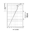
- FIG. 46 is a diagram showing a loop transfer function
- FIG. 47 is a block diagram of improved surface topography learning with PTC (STL-PTC);
- FIG. 48 is a diagram showing a signal generator
- FIG. 49 is a block diagram of a surface topography learning observer (STLO);
- FIG. 50 is a diagram showing a frequency response from a Q filter
- FIG. 51 is a diagram showing a frequency response from the Q filter
- FIG. 52 is a diagram showing the results of simulation of scanning of a rectangular wave-like sample surface
- FIG. 53 is a diagram showing the results of simulation of scanning of the rectangular wave-like sample surface
- FIG. 54 is a diagram showing the results of simulation of scanning of the rectangular wave-like sample surface
- FIG. 55 is a diagram showing the results of simulation of scanning of the rectangular wave-like sample surface
- FIG. 56 is a diagram showing the shape of a grating element
- FIG. 57 is a diagram showing standard deviations
- FIG. 58 is a diagram showing a waveform in which error signals are superimposed on one another
- FIG. 59 is a diagram showing a waveform in which error signals are superimposed on one another
- FIG. 60 is a diagram showing a waveform in which error signals are superimposed on one another
- FIG. 61 is a diagram showing a waveform in which error signals are superimposed on one another
- FIG. 62 is a diagram showing a waveform in which error signals are superimposed on one another
- FIG. 63 is a diagram showing a waveform in which error signals are superimposed on one another
- FIG. 64 is a diagram showing an image of a sample measured with the AFM
- FIG. 65 is a diagram showing an image of the sample measured with the AFM
- FIG. 66 is a diagram showing an image of the sample measured with the AFM
- FIG. 67 is a diagram showing an image of the sample measured with the AFM
- FIG. 68 is a diagram showing the sectional waveform of the sample measured with the AFM
- FIG. 69 is a diagram showing the sectional waveform of the sample measured with the AFM.
- FIG. 70 is a diagram showing the sectional waveform of the sample measured with the AFM.
- FIG. 71 is a diagram showing the sectional waveform of the sample measured with the AFM
- FIG. 72 is a diagram showing an image of a sample measured with the AFM
- FIG. 73 is a diagram showing an image of the sample measured with the AFM
- FIG. 74 is a diagram showing an image of the sample measured with the AFM
- FIG. 75 is a diagram showing an image of the sample measured with the AFM.
- FIG. 76 is a diagram showing the sectional waveform of the sample measured with the AFM.
- FIG. 77 is a diagram showing the sectional waveform of the sample measured with the AFM.
- FIG. 78 is a diagram showing the sectional waveform of the sample measured with the AFM.
- FIG. 79 is a diagram showing the sectional waveform of the sample measured with the AFM.
- FIG. 80 is a diagram showing frequency characteristics
- FIG. 81 is a diagram showing frequency characteristics
- FIG. 82 is a diagram showing frequency characteristics
- FIG. 83 is a diagram showing frequency characteristics
- FIG. 84 is a diagram showing a control mechanism according to the present embodiment.
- FIG. 85 is a diagram showing the results of simulation
- FIG. 86 is a diagram showing the results of simulation
- FIG. 87 is a diagram showing the results of simulation
- FIG. 88 is a diagram showing the results of simulation
- FIG. 89 is a diagram showing frequency characteristics
- FIG. 90 is a diagram showing frequency characteristics
- FIG. 91 is a diagram showing frequency characteristics
- FIG. 92 is a diagram showing frequency characteristics
- FIG. 93 is a diagram showing an image of a sample measured with the AFM.
- FIG. 94 is a diagram showing an image of the sample measured with the AFM
- FIG. 95 is a diagram showing an image of the sample measured with the AFM.
- FIG. 96 is a diagram showing a waveform in which error signals are superimposed on one another
- FIG. 97 is a diagram showing a waveform in which error signals are superimposed on one another
- FIG. 98 is a diagram showing a waveform in which error signals are superimposed on one another
- FIG. 99 is a diagram showing the results of simulation.
- FIG. 100 is a diagram showing the results of simulation
- FIG. 101 is a diagram showing the results of simulation
- FIG. 102 is a diagram showing the results of simulation
- FIG. 103 is a diagram showing a signal generator
- FIG. 104 is a diagram showing the results of simulation
- FIG. 105 is a diagram showing the results of simulation
- FIG. 106 is a diagram showing the results of simulation
- FIG. 107 is a diagram showing the results of simulation
- FIG. 108 is a diagram showing the results of simulation.
- FIG. 109 is a diagram showing the results of simulation.
- FIG. 1 is a schematic diagram showing an AFM 100 according to the present invention by way of example.
- a probe 102 attached to a cantilever 101 performs scanning along a sample surface 103 to measure deflection of the cantilever 101 caused by an atomic force exerted between the sample surface 103 and the probe 102 as well as distortion of the cantilever 101 caused by a friction force exerted between the sample surface 103 and the probe 102 .
- the structure of the sample surface 103 is measured on a nano-scale.
- laser light provision means 110 allows laser light 104 to obliquely enter the rear surface of the cantilever 101 . Then, a change in the reflection angle of the laser light 104 caused by displacement of cantilever 101 resulting from deflection and distortion thereof is detected based on a relative change in the intensity of laser light 106 entering a four-piece photodiode 105 . Finally, the AFM 100 can detect the deflection and distortion of the cantilever 101 based on a change in the intensity of the laser light 106 to measure the structure of the sample surface 103 .
- the apparatus detecting a relative change in the intensity of the laser light 106 is not limited to the four-piece photodiode but may be light detection means capable of detecting a relative change in the intensity of the laser beam.
- a visible-light semiconductor laser may be used as the laser light provision means 110 .
- a controller 108 controls a piezo 107 so as to maintain the displacement of the cantilever 101 constant.
- An output from the controller 108 is converted, and the converted output is recorded in the data storage means 109 as the surface topography of the sample surface 103 .
- Schemes of measuring the “displacement of the cantilever” caused by surface recesses and protrusions include a scheme of measuring the interference of the laser light (light interference scheme) and a light leverage scheme of measuring a change in the reflection angle of the laser light caused by the displacement of the cantilever.
- the present embodiment uses the light leverage scheme, which is more common.
- the light leverage scheme measures a relative change in the intensity of light entering diodes 1 to 4.
- the light leverage scheme is based on the deflection of the tip of the leverage (the tip of the cantilever) in a Y direction and the twist of the tip of the leverage in an X direction.
- a relative change (1+2) ⁇ (3+4) is detected.
- a relative change (1+4) ⁇ (2+3) is detected.
- the friction force is measured.
- the microscope is called an FEM (Friction Force Microscope) instead of the AFM.
- the AFM according to the present embodiment measures only the deflection and thus corresponds to the former AFM detection method.
- a model of the AFM is based on the cantilever and the interaction between the probe and the sample.
- Such a model as shown in FIG. 2 is adopted (see Non-Patent Documents 1 and 7).
- the contact mode is used for measurement in order to simplify the modeling.
- the spring coefficient of a spring 203 is defined as k 1
- the natural length of the spring 203 is defined as L 10
- the spring coefficient of a spring 201 is defined as k 2
- the natural length of the spring 201 is defined as L 20 .
- reference character (b) denotes the damper coefficient of a friction force generation source 205 .
- the current lengths of the springs 203 and 201 are defined as L 1 and L 2 , respectively.
- Reference character (u) denotes a manipulating quantity for the piezo.
- Reference character (d) denotes the recesses and protrusions of the sample. In this case, the interaction between the sample and the cantilever is expressed as shown in FIG. 2 .
- F(t) denotes a force that the cantilever receives from the spring 201 , that is, an atomic force from the sample.
- Non-Patent Document 1 indicates that based on the model, the recesses and protrusions of the sample can be modeled as an input disturbance.
- the displacement (y) of the cantilever is measured using the photodiode and laser light.
- the displacement (y) is determined by multiplying a transfer function for a plant by a given gain (g). The relationship between the gain (g) and the output will be described in the next chapter.
- the details of a method for deriving Formula (1) are described in, for example, Non-Patent Document 1.
- the AFM according to the present invention may be constructed by connecting an interface for required input signals to a JSPM-5200 manufactured by JEOL Ltd. and using a controller board such as a Dspace 1104 to improve an algorithm and hardware for a control system.
- a controller board such as a Dspace 1104 to improve an algorithm and hardware for a control system.
- the details of the algorithm for the control system are described in, for example, Non-Patent Documents 8 and 9.
- FIG. 3 is a block diagram showing the flow of signals in the AFM according to the present invention.
- the displacement of the cantilever 101 is output by the PD (PhotoDiode) 105 .
- This signal is converted by an AD 305 , and the resulting signal is input to a DSP (Digital Signal Processor) as y[i].
- a DA 301 converts a manipulating quantity u[i]
- an amplifier 302 amplifies the converted manipulating quantity u[i].
- the amplified signal is applied to the PZT (piezo) 107 as a driving voltage.
- the gain of AD/DA in the DSP is adjusted to 1.
- An output x [V] from the PD is output as a voltage indicating the displacement of the cantilever and varying depending on a force curve.
- a relational expression for the driving voltage for the PZT and the output from the PD is determined based on the force curve.
- K PD 3.61 ⁇ 10 ⁇ 2 [V/nm].
- the K PD is determined from the first-order approximation of measurement data of the force curve obtained by the JSPM-5200.
- the force curve is described in, for example, Non-Patent Document 1.
- a model is estimated using a least squares method based on experimentally obtained I/O data.
- an M-sequence signal is used as an identification input (pseudo disturbance).
- An ARX model is used to estimate a model (see Non-Patent Document 8).
- transfer functions at discrete times are each expressed by a second-order denominator and a first-order numerator.
- a zeroth-order hold is used to convert the transfer functions into a continuous time.
- a transfer function from formula (1) can be expressed as formula (2).
- the M-sequence signal cannot be provided directly to the cantilever, so that in FIG. 3 , the M-sequence signal is input to the PZT via the DA 301 , with estimation performed based on an output from the AD 305 .
- FIG. 8 is a Bode diagram in which the frequency characteristics of a plant in the above-described model based on formula (2) are compared with those identified by a servo analyzer.
- the identified plant exhibits a significant resonance at 5,610 [Hz] and has a high gain even in a low frequency region.
- FIG. 9 shows a comparison of a temporal variation in voltage observed with the AFM according to the present invention, with a temporal variation in voltage provided by the above-described model.
- FIG. 9 shows that model outputs allow measurement outputs (actual outputs) to be reproduced to some degree.
- a controller used for comparison with the proposed method is provided in an actual product.
- the controller is defined as a conventional method.
- An expression for the controller is given as follows.
- FIG. 10 shows a loop transfer function for the plant and the controller.
- FIG. 10 shows that the conventional method has a cutoff frequency of 252 [Hz], indicating that proportional control and a low pass filter can deal with up to this frequency band.
- a gain margin is 14.3 [dB]
- a phase margin is 89.5 [deg].
- FIG. 11 is a block diagram of estimation in the STO.
- ⁇ circumflex over (d) ⁇ [Expression 4] is obtained by passing a signal passed through the inverse model of a nominal plant: P n ⁇ 1 ( s ) [Expression 5] and from which the manipulating quantity u(t) is subtracted, through a low pass filter Q(s) for the cutoff frequency ⁇ c .
- FIG. 11 is a block diagram of estimation in the STO. In FIG.
- an estimation block 1102 in an estimation block 1100 is characterized by being implemented as a disturbance observer for an open loop independently of a feedback loop 1101 .
- a surface topography 703 is considered to be an input end disturbance d(t) at time (t).
- the estimated value for the surface topography is obtained from an output 1104 .
- this special disturbance observer is referred to as a surface topography observer (STO).
- STO is composed of an open loop and is thus not limited to the frequency band of a closed loop.
- the frequency band of Q(s) can be increased up to a Nyquist frequency.
- the STO described in the preceding chapter is composed of an open loop.
- increasing the frequency band of Q(s) above that of a closed loop is considered to be preferable.
- an error in the modeling of the plant increases owing to a Lennard-Jones potential (see Non-Patent Document 1).
- adjusting the tracking error (e) to 0 resulting in a modeling error is expected to avoid the disadvantages of the STO. Consequently, the present embodiment applies a PTC method to allow a target trajectory (described below) generated from the learned tracking error (e) to be perfectly tracked. Therefore, the tracking error (e) is reduced in a feedforward manner, thus improving the control performance.
- the PTC method corresponds to a two-degree-of-freedom control system in which a sampling period T r for the target trajectory is different from a control period T u for the target trajectory.
- a control input is switched (n) times at the intervals of T u .
- (n) denotes the order of the plant.
- the feedforward controller becomes unstable under the effect of unstable zeroes generated when the plant based on a linear continuous-time system is discretized at a short sampling period. Therefore, multirate control allows the feedforward controller to create the stable reverse system of the plant (see Non-Patent Document 5).
- the surface topography learning with PTC involves measuring and storing a tracking error during a forward scan and using the stored tracking error to increase tracking accuracy during a backward scan.
- Non-Patent Document 6 Although a repetitive PTC method of reducing a possible periodic disturbance for every sample point is applicable, selecting only samples with periodic surface topographies for measurements by the AFM is impossible.
- the surface topography learning with PTC learns and controls the surface of the sample during the forward and backward scans.
- a grating element is used to observe the sample.
- any element other than the grating element are applicable.
- FIG. 12 is a block diagram of STL-PTC.
- a surface topography 1201 is input, and an estimated surface topography is stored in data storage means 1202 .
- reference numeral 1203 denotes a signal generator, and reference numeral 1204 denotes a switch.
- the manipulating quantity (u) indicates surface topography data. Since the set point is zero, an output (voltage) (y) is an error signal (e).
- a smaller value of the error signal (e) means a more accurate image resulting from the current manipulating quantity (u). That is, the error signal (e) corresponds to a tracking error used for the surface topography learning with PTC.
- FIG. 6 shows a surface scan path of the probe of the AFM according to the present invention.
- a CPU mounted in the AFM according to the present invention reads and executes a program stored in a storage device to perform the STL-PTC.
- the probe performs a rightward X-direction scan over a scan width from a start position.
- the probe then performs a leftward X-direction scan along the scan path to return to the scan start position.
- the probe similarly performs a scan in the Y direction.
- a surface scan is achieved.
- the rightward scan in the X direction is called a forward scan (FWS).
- the leftward scan in the X direction is called a backward scan (BWS).
- the two scans allow the image to be measured. Provided that the probe follows the same path both during the FWS and during the BWS, error signals appearing during the scans are ideally exactly the same.
- error signals are measured and stored and then learned, and based on the learned error signals, learning control is performed so as to cancel a possible error signal during the BWS. Consequently, error signals (e) (tracking errors) for feedback control can be reduced to improve the tracking capability.
- FIG. 5 shows a procedure of control for the AFM according to the present invention.
- an X scan waveform is triangular.
- Each image is measured during an FWS 501 and during a BWS 502 .
- Error signals are stored in a signal generator composed of a stack memory 1301 shown in FIG. 13 .
- a switch 2 (SW 2 ) is turned on to allow the signal generator to generate a target trajectory allowing the error to be adjusted to 0. Then, the PTC adjusts the error to 0.
- the N m memory rows can serve as a feedforward compensator. This enables possible error signals to be reduced for every sample point.
- the signal generator provides no output.
- reference numerals 504 , 506 , and 508 denote learning processes.
- Reference numerals 505 , 507 , and 509 denote control processes.
- the STO is an open loop, and a modeling error may thus degrade the robustness of the STO.
- the proposed method compensates for the degraded robustness by the feedback control.
- the PTC method is based on multirate control provided by a feedforward controller and a feedback controller to achieve perfect tracking in contrast to a method based on single-rate control (see Non-Patent Document 5).
- FIG. 14 to FIG. 17 show disturbances estimated by the conventional method and the observer, as simulation of a rectangular wave-like sample.
- FIG. 14 shows a complementary sensitivity function obtained by the conventional method.
- FIG. 15 is a diagram showing the results of simulation of an output voltage obtained when the AFM according to the present invention adopts the conventional method to scan a rectangular wave-like sample surface.
- FIG. 16 is a diagram showing a frequency response from Q(s) in the STO.
- FIG. 17 is a diagram showing the results of simulation of an output voltage obtained when the AFM according to the present invention adopts the STO to scan the rectangular wave-like sample surface.
- FIG. 14 shows that the conventional method limits the poles of the closed loop to the resonant frequency of the plant.
- FIG. 16 shows that the observer of the STO does not depend on the resonant frequency of the plant but depends on the poles of the low pass filter unless the observer is limited by the Nyquist frequency.
- the estimated value: ⁇ circumflex over (d) ⁇ [Expression 23] in FIG. 17 allows the surface topography (d) of the sample to be accurately reproduced.
- FIGS. 18A and 18B show the shape and size of a grating element 1801 observed with the AFM according to the present invention.
- a grating element may be, by way of example, a planar brazed holographic grating standard article manufactured by Shimadzu Corporation.
- the grating element shown in FIG. 18A and FIG. 18B is characterized by being shaped like saw teeth-like grooves. Grating grooves are formed on a glass substrate of resin. The grooves are coated with a reflection film of Al or the like.
- the sampling frequency of a DSP in the AFM according to the present invention is set to 10 [kHz] by way of example. Then, the results described below were obtained.
- FIG. 25 shows an image of the surface of the above-described grating element obtained by allowing the AFM according to the present invention to scan the surface of the grating element using the conventional method.
- FIG. 26 shows an image of the surface the above-described grating element obtained by allowing the AFM according to the present invention to scan the surface of the grating element using the STO.
- FIG. 27 shows an image of the surface the above-described grating element obtained by allowing the AFM according to the present invention to scan the surface of the grating element using the STL-PTC.
- scanning speed is 32.2 ⁇ m/s.
- FIG. 28 is a histogram of the frequency of the height of recesses and protrusions on the surface of the above-described grating element obtained by allowing the AFM according to the present invention to scan the surface of the grating element using the conventional method under the same conditions as those in FIG. 25 .
- FIG. 29 is a histogram of the frequency of the height of recesses and protrusions on the surface of the above-described grating element obtained by allowing the AFM according to the present invention to scan the surface of the grating element using the STO under the same conditions as those in FIG. 26 .
- FIG. 30 is a histogram of the frequency of the height of recesses and protrusions on the surface of the above-described grating element obtained by allowing the AFM according to the present invention to scan the surface of the grating element using the STL-PTC under the same conditions as those in FIG. 27 .
- FIG. 31 shows a sectional waveform of the above-described grating element obtained by allowing the AFM according to the present invention to scan the surface of the grating element using the conventional method under the same conditions as those in FIG. 25 .
- FIG. 32 shows a sectional waveform of the above-described grating element obtained by allowing the AFM according to the present invention to scan the surface of the grating element using the STO under the same conditions as those in FIG. 26 .
- FIG. 33 shows a sectional waveform of the above-described grating element obtained by allowing the AFM according to the present invention to scan the surface of the grating element using the STL-PTC under the same conditions as those in FIG. 27 .
- FIG. 34 shows an image of the surface of the above-described grating element obtained by allowing the AFM according to the present invention to scan the surface of the grating element using the conventional method.
- FIG. 35 shows an image of the surface of the above-described grating element obtained by allowing the AFM according to the present invention to scan the surface of the grating element using the STO.
- FIG. 36 shows an image of the surface of the above-described grating element obtained by allowing the AFM according to the present invention to scan the surface of the grating element using the STL-PTC.
- scanning speed is 161 ⁇ m/s.
- FIG. 37 is a histogram of the frequency of the height of recesses and protrusions on the surface of the above-described grating element obtained by allowing the AFM according to the present invention to scan the surface of the grating element using the conventional method under the same conditions as those in FIG. 34 .
- FIG. 38 is a histogram of the frequency of the height of recesses and protrusions on the surface of the above-described grating element obtained by allowing the AFM according to the present invention to scan the surface of the grating element using the STO under the same conditions as those in FIG. 35 .
- FIG. 39 is a histogram of the frequency of the height of recesses and protrusions on the surface of the above-described grating element obtained by allowing the AFM according to the present invention to scan the surface of the grating element using the STL-PTC under the same conditions as those in FIG. 36 .
- FIG. 40 shows a sectional waveform of the above-described grating element obtained by allowing the AFM according to the present invention to scan the surface of the grating element using the conventional method under the same conditions as those in FIG. 34 .
- FIG. 41 shows a sectional waveform of the above-described grating element obtained by allowing the AFM according to the present invention to scan the surface of the grating element using the STO under the same conditions as those in FIG. 35 .
- FIG. 42 shows a sectional waveform of the above-described grating element obtained by allowing the AFM according to the present invention to scan the surface of the grating element using the STL-PTC under the same conditions as those in FIG. 36 .
- FIGS. 28 , 30 , 37 , and 39 relate to the height of the sample determined from the manipulating quantity u(t).
- the histograms shown in FIGS. 29 and 38 relate to the height of the sample determined from the estimated value: ⁇ circumflex over (d) ⁇ [Expression 24]
- FIG. 31 to FIG. 33 and FIG. 40 to FIG. 42 show a waveform obtained by superimposing the 10 cross sections in the images in FIG. 25 to FIG. 27 , and FIG. 34 to FIG. 36 on one another at intervals of 0.125 ⁇ m.
- the scanning speed indicates the speed of scanning in the (x) direction shown in FIG. 6 .
- Scan range is 5.5 ⁇ m ⁇ 5.5 ⁇ m both for a scanning speed of 32.2 ⁇ m/s and for a scanning speed of 161 ⁇ m/s. Time required for the whole scan is about 3 minutes and about 40 seconds, respectively.
- FIG. 25 to FIG. 27 are enlarged views of images obtained at a scanning speed of 32.2 ⁇ m/s.
- FIG. 34 to FIG. 36 are enlarged views of images obtained at a scanning speed of 161 ⁇ m/s. The range for the enlarged images is 1.6 ⁇ m ⁇ 1.6 ⁇ m.
- the histogram for the conventional method in FIG. 37 shows an extremely small number of height rates.
- the histogram for the STO shows a relatively large number of height rates.
- the sectional waveform for the STO shown in FIG. 41 shows more rugged recesses and protrusions than that for the conventional method shown in FIG. 32 .
- the u(t) exhibits a significantly degraded property of tracking the surface of the sample. This means that the STO is likely to increase the modeling error to degrade the image. This is also indicated by the fact that images obtained using the STO and shown in FIG. 35 are more significantly degraded than those obtained using the STL-PTC and shown in FIG. 36 and that the STL-PTC is thus superior to the STO.
- FIGS. 21 and 24 show a comparison of the conventional method with the STL-PTC, with error signals evaluated in terms of ⁇ 3 ⁇ .
- FIGS. 21 and 24 show that “without learning control” indicates the results for the conventional method, whereas “with learning control” indicates the results for the STL-PTC.
- FIG. 21 shows the case of a scanning speed of 32.2 ⁇ m/s and indicates 4.53% improvement with respect to the height of the recesses and protrusions (60 nm).
- FIG. 24 shows the case of a scanning speed of 161 ⁇ m/s and indicates 52.5% improvement with respect to the height of the recesses and protrusions (60 nm).
- FIGS. 19 , 20 , 22 , and 23 shows superimposed relationships between error signals and data points (data acquisition points) within one image.
- the above-described embodiment of the present invention indicates the difference between the conventional method and the STO and thus the advantages of the STO over the conventional method.
- the STO is not robust to errors in the modeling of the plant.
- a large modeling error occurs.
- images obtained using the STL-PTC are less degraded than those obtained using the STO. This is because the STL-PTC allows possible tracking errors to be reduced by the PTC, while allowing modeling errors to be compensated for through feedback, enabling the disadvantages of the STO associated with a rapid change in the recess and protrusion to be avoided.
- a model based on a contact mode for the interaction between a sample surface 103 and the tip 102 of a cantilever is used to give a motion equation for the tip of the cantilever with a mass (m), as shown in formula (1).
- Non-Patent Document 2 can be used to convert the above-described model into one to which the recesses and protrusions on the sample surface 103 are input.
- a transfer function for the plant according to the present embodiment is identified as follows according to a method of system identification described in Non-Patent Document 9.
- FIGS. 43 and 44 show a comparison of the frequency characteristics of a plant based on formula (17) with frequency characteristics identified by a servo analyzer (manufactured by ONO SOKKI Co., Ltd.). The figures show that the plant identified as shown in formula (17) resonates significantly at 5,590 [Hz] and provides a high gain even in a low frequency region.
- the AFM according to the present embodiment is a special model of a JSPM-5200 manufactured by JEOL Ltd. However, this is only an example, and any AFM is applicable provided that the present embodiment can be incorporated into the AFM.
- dSPACE1104 may be used to modify a control mechanism for the AFM so that the control mechanism allows the present embodiment to be implemented.
- FIG. 3 is a block diagram showing the flow of signals inside the AFM according to the present embodiment.
- the displacement of the tip 102 of the cantilever is detected by a PD (four-piece PhotoDiode) 105 and is output as a signal.
- the signal is subjected to AD conversion by an AD (AD converter) 305 .
- the resulting signal is input to a DSP (Digital Signal Processor) as y[i].
- an output x [V] from the PD (four-piece PhotoDiode) 105 is provided according to a force curve (the relation expression between a force exerted on the tip of the cantilever and the distance between the cantilever tip and the sample).
- K PD 2.44 ⁇ 10 ⁇ 2 [V/nm].
- K PD is determined by first-order-approximating the measurement data of the force curve (Non-Patent Document 2) obtained with the JSPM-5200, by way of example.
- a manipulating quantity u[i] resulting from DA conversion by the DA (DA converter) 301 in the DSP is amplified by an amplifier 302 .
- the amplified manipulating quantity u[i] is applied to a PZT (piezo) 107 as a driving voltage.
- the gain of the AD/DA in the DSP is adjusted to 1.
- the controller according to the conventional method to be compared with the embodiment of the present invention is a phase delay compensator used in a product.
- a transfer function for the controller according to the conventional method is as shown in formula (3).
- FIGS. 45 and 46 show loop transfer functions for the plant and the controller.
- FIG. 46 shows that the cutoff frequency of the controller according to the conventional method is 177 [Hz].
- Non-Patent Document 11 proposes the surface topography learning with PTC (STL-PTC).
- the present embodiment uses an improved STL-PTC obtained by improving the surface topography learning with PTC proposed in Non-Patent Document 11.
- the learning algorithm of the improved STL-PTC is used to perform perfect tracking based on the learned tracking error (e), thus enabling a surface image observed with the AFM to be accurately estimated.
- FIG. 47 is a block diagram of the improved STL-PTC.
- a surface topography 4701 is input, and an estimated surface topography is stored in data storage means 4702 .
- the improved STL-PTC performs scanning using an output signal (error) during an FWS as a command value for a BWS.
- the improved STL-PTC thus requires a signal generator 4703 including a stack memory in which data obtained at the end of the FWS is saved as the first data for the BWS.
- the block diagram shown in FIG. 47 is characterized in that a calculation 4704 includes a discretized nominal plant P n [z]. Installation of such a disturbance estimation mechanism matches the dynamics of an output signal during the FSW with the dynamics of an output signal during the BWS.
- FIG. 48 is a diagram showing the details of the signal generator 4703 .
- An output end conversion value: P ( s ) ⁇ circumflex over (d) ⁇ [Expression 26] for a disturbance estimated value obtained by the disturbance estimation mechanism shown in FIG. 47 passes through a stack memory 4801 and is stored in a stack memory 1301 .
- the output end conversion value: P ( s ) ⁇ circumflex over (d) ⁇ [Expression 27] stored in the stack memory passes through a sensitivity function 4802 :
- the switch 2 (SW 2 ) is turned on to allow the signal generator to generate a target trajectory allowing the error to be adjusted to 0. Then, the PTC adjusts the error to 0.
- the N d memory rows can serve as a feedforward compensator. This enables possible error signals to be reduced for every sample point.
- the signal generator provides no output.
- reference numerals 1104 , 1106 , and 1108 denote learning processes.
- Reference numerals 1105 , 1107 , and 1109 denote control processes.
- the STL-PTC includes a complicated control mechanism and the dynamics of the plant P n [z].
- a learning signal does not perfectly match the error signal during the BWS.
- the present embodiment also uses a surface topography learning observer (STLO).
- STLO applies the reverse system of a discretized plant to estimate a disturbance, and reduces the possible disturbance in a feedforward manner without affecting the stability of the system.
- a surface image observed with the AFM can be accurately estimated.
- the STLO like the STL-PTC, need not estimate the disturbance in real time.
- creating the reverse system of the plant delayed by one sample enables the disturbance (d) to be reduced at intervals of the control period T u (0.1 msec).
- the disturbance is estimated by a zeroth-order disturbance observer, so that for any waveform, the disturbance theoretically delayed by one sample cannot always be estimated.
- FIG. 49 is a block diagram showing control performed by the STLO.
- a surface topography 4901 is input, and an estimated surface topography is stored in data storage means 4902 .
- the block diagram shown in FIG. 49 is characterized in that a calculation 4904 includes the reciprocal P ⁇ 1 n [z] of the discretized nominal plant P n [z].
- the disturbance that estimated with one-sample delay based on the reverse system of the discretized plant; ⁇ circumflex over (d) ⁇ [Expression 31] allows the SW 1 to be kept on for T seconds during the FWS.
- the relevant data is saved to a stack memory 4903 .
- the stack memory delays the output of the estimated disturbance by one sample. This enables the disturbance: ⁇ circumflex over (d) ⁇ [Expression 32] during the BWS to be reduced for every sample point.
- the feedback controller C[z] if an error or a modeling error following compensation or a disturbance not present during the FWS is input during the BWS, this is compensated for by the feedback controller C[z].
- a low pass filter Q[z] with no phase delay is introduced in order to cut noise.
- This is called a Q filter (Non-Patent Document 16).
- FIGS. 50 and 51 a frequency response from the Q filter is shown in FIGS. 50 and 51 .
- FIGS. 52 and 53 show the results of simulation in which a rectangular wave-like sample surface is scanned.
- the period before 0.02 sec corresponds to the results of simulation of the conventional method
- the period after 0.02 sec corresponds to the results of simulation of the improved STL-PTC.
- FIG. 52 shows a temporal variation in the manipulating quantity u(t) of the piezo.
- FIG. 53 shows a temporal variation in output signal y(t).
- FIGS. 54 and 55 show the results of simulation in which a rectangular wave-like sample surface is scanned.
- the period before 0.02 sec corresponds to the results of simulation of the conventional method
- the period after 0.02 sec corresponds to the results of simulation of the STLO.
- FIG. 54 shows a temporal variation in the manipulating quantity u(t) of the piezo.
- FIG. 55 shows a temporal variation in output signal y(t).
- the sampling time T r for the command value (the signal saved to the stack memory for learning) is 0.2 msec (milliseconds (10 ⁇ 3 seconds)).
- the compensation fails to be achieved between the sample points for the sampling time T y (0.1 msec) for the output signal. Consequently, in FIG. 53 , an error occurs after 0.02 sec.
- the disturbance forms a step to affect the plant.
- the signal: P ( s ) ⁇ circumflex over (d) ⁇ [Expression 39] learned during the FWS disadvantageously degrades the signal for the BWS.
- six Q filters are installed along the target trajectory to reduce this adverse effect.
- the sample is, by way of example, a planar brazed holographic grating standard article manufactured by Shimadzu Corporation.
- the grating element is shaped like a rectangular wave, and includes a glass substrate of resin with grating grooves formed therein. The grooves are coated with a reflection film of Al or the like.
- FIG. 56 shows the shape and size of a grating element 5601 observed with the AFM according to the present embodiment.
- FIG. 64 shows an image obtained by allowing the AFM to scan the surface of the grating element 5601 using the conventional method.
- FIG. 65 shows an image obtained by allowing the AFM to scan the surface of the grating element 5601 using the STO.
- FIG. 66 shows an image obtained by allowing the AFM to scan the surface of the grating element 5601 using the improved STL-PTC.
- FIG. 67 shows an image obtained by allowing the AFM to scan the surface of the grating element 5601 using the STLO.
- FIG. 68 shows a sectional waveform obtained by allowing the AFM to scan the surface of the grating element 5601 using the conventional method.
- FIG. 69 shows a sectional waveform obtained by allowing the AFM to scan the surface of the grating element 5601 using the STO.
- FIG. 70 shows a sectional waveform obtained by allowing the AFM to scan the surface of the grating element 5601 using the improved STL-PTC.
- FIG. 71 shows a sectional waveform obtained by allowing the AFM to scan the surface of the grating element 5601 using the STLO.
- the poles of the low pass filter of the STO are at 2,000 Hz.
- the scan range of the AFM is 5.5 ⁇ m ⁇ 5.5 ⁇ m ( FIG. 64 to FIG. 67 are enlarged views of a scan area of 3 ⁇ m ⁇ 3 ⁇ m).
- the scanning speed of the AFM is 32.2 ⁇ m/sec.
- FIG. 72 shows an image obtained by allowing the AFM to scan the surface of the grating element 5601 using the conventional method.
- FIG. 73 shows an image obtained by allowing the AFM to scan the surface of the grating element 5601 using the STO.
- FIG. 74 shows an image obtained by allowing the AFM to scan the surface of the grating element 5601 using the improved STL-PTC.
- FIG. 75 shows an image obtained by allowing the AFM to scan the surface of the grating element 5601 using the STLO.
- FIG. 76 shows a sectional waveform obtained by allowing the AFM to scan the surface of the grating element 5601 using the conventional method.
- FIG. 77 shows a sectional waveform obtained by allowing the AFM to scan the surface of the grating element 5601 using the STO.
- FIG. 78 shows a sectional waveform obtained by allowing the AFM to scan the surface of the grating element 5601 using the improved STL-PTC.
- FIG. 79 shows a sectional waveform obtained by allowing the AFM to scan the surface of the grating element 5601 using the STLO.
- the poles of the low pass filter of the STO are at 2,000 Hz.
- the scan range of the AFM is 5.5 ⁇ m ⁇ 5.5 ⁇ m ( FIG. 72 to FIG. 75 are enlarged views of a scan area of 3 ⁇ m ⁇ 3 ⁇ m).
- the scanning speed of the AFM is 322 ⁇ m/sec.
- FIG. 64 A comparison of FIG. 64 ( FIG. 68 ) with FIG. 72 ( FIG. 76 ) indicates that with the conventional method, increasing the scanning speed of the AFM significantly degrades the image. Furthermore, a comparison of FIG. 72 ( FIG. 76 ) with FIG. 73 (FIG. 77 ) indicates that with the STO, the degradation of the image is reduced even with an increase in the scanning speed of the AFM. However, FIG. 73 indicates that when the scanning speed of the AFM is increased for high-speed scanning, then even with the STO, the high-speed scanning causes the tracking capability of the u(t) to be significantly degraded. In this case, the modeling error increases, preventing the rectangular wave-like shape from being accurately shaped.
- FIG. 74 indicates that the surface topography imaged by the improved STL-PTC is nearer rectangular than that imaged by the STO. This is expected to be because the feedforward compensation reduces possible error signals to improve the tracking capability of the u (t). However, even with the improved STL-PTC, the modeling error and the inter-sample-point response make the surface topography in the image appear larger than the actual one having the desired pitch.
- the STLO cancels the disturbance in a feedforward manner based on the estimated one.
- the STLO compensates for the modeling error through feedback to improve the tracking capability of the u(t) compared to the improved STL-PTC. Consequently, FIG. 75 ( FIG. 79 ) shows that the STLO allows the rectangular wave-like shape to be accurately imaged.
- FIG. 57 shows ⁇ 3 ⁇ for the conventional method, the improved STL-PTC, and the STLO.
- the standard deviation indicates evaluation for error signals obtained through about 100 scans.
- FIG. 58 to FIG. 63 show waveforms each obtained by superimposing the above-described error signals on one another.
- FIG. 58 to FIG. 60 show error signals obtained when the scanning speed of the AFM is 32.2 ⁇ m/sec.
- FIG. 58 shows error signals obtained when the AFM uses the conventional method.
- FIG. 59 shows error signals obtained when the AFM uses the improved STL-PTC.
- FIG. 60 shows error signals obtained when the AFM uses the STLO.
- FIG. 61 to FIG. 63 show error signals obtained when the scanning speed of the AFM is 322 ⁇ m/sec.
- FIG. 61 shows error signals obtained when the AFM uses the conventional method.
- FIG. 62 shows error signals obtained when the AFM uses the improved STL-PTC.
- FIG. 63 shows error signals obtained when the AFM uses the STLO.
- the improved STL-PTC improves the ⁇ 3 ⁇ by 54.6% compared to the conventional method.
- the STLO improves the ⁇ 3 ⁇ by 68.1% compared to the conventional method.
- the improved STL-PTC improves the ⁇ 3 ⁇ by 69.8% compared to the conventional method.
- the STLO improves the ⁇ 3 ⁇ by 81.0% compared to the conventional method.
- the present embodiment includes a simple identification method for the STLO which uses a low-order model to allow the frequency characteristics of a plant to be easily identified, and an STLO improved by using zeroth-order phase error inverse model (ZPEI).
- ZPEI zeroth-order phase error inverse model
- the AFM according to the present embodiment is a special model of a JSPM-5200 manufactured by JEOL Ltd. However, this is only an example, and any AFM is applicable provided that the present embodiment can be incorporated into the AFM.
- dSPACE1104 may be used to modify the control mechanism for the AFM so that the control mechanism allows the present embodiment to be implemented.
- FIG. 3 is a block diagram showing the flow of signals inside the AFM according to the present embodiment.
- a sample surface 103 when a sample surface 103 is scanned, the displacement of the tip 102 of the cantilever is detected by a PD (four-piece PhotoDiode) 105 and is output as a signal.
- the signal is subjected to AD conversion by an AD (AD converter) 305 .
- the resulting signal is input to a DSP (Digital Signal Processor) as y [i].
- DSP Digital Signal Processor
- an output x [V] from the PD (four-piece PhotoDiode) is provided according to a force curve (the relation expression between a force exerted on the tip of the cantilever and the distance between the cantilever tip and the sample).
- K PD 4.2804 ⁇ 10 ⁇ 2 [V/nm].
- K PD is determined by first-order-approximating the measurement data of the force curve (Non-Patent Document 2) obtained with the JSPM-5200, by way of example.
- a manipulating quantity u[i] resulting from DA conversion by a DA (DA converter) 301 in the DSP is amplified by an amplifier 302 .
- the amplified manipulating quantity u[i] is applied to a PZT (piezo) 107 as a driving voltage.
- the gain of the AD/DA in the DSP is adjusted to 1.
- a motion equation as shown in formula (1) is given for the tip 102 of the cantilever with a mass (m), using a model based on a contact mode and relating to the interaction between the sample surface 103 and the tip 102 of the cantilever as shown in FIG. 2 .
- the model may use recesses and protrusions on the sample surface 103 as an input disturbance according to the method described in Non-Patent Document 2.
- the displacement (y) of the cantilever is measured using the photodiode and laser light.
- the transfer function for the plant is multiplied by a given gain (g).
- formula (1) is identified as described below.
- the simple identification method performs fitting based on a frequency response from a standard second-order system determined on the basis of frequency characteristics identified when an identification input is a swept sine.
- the identification algorithm of the simple identification method will be described.
- a transfer function for the standard second-order system is:
- the amplitude value of Equation (22) may be determined.
- ⁇ p ⁇ square root over (1 ⁇ 2 ⁇ 2 ) ⁇ n
- the peak width M p of the gain shown in formula (23) can be obtained.
- g m denotes a peak gain
- g s denotes a DC gain.
- a general form of the standard second-order system is obtained by making a program such that the DC gain, the peak gain, and the peak frequency are automatically acquired from the experimentally obtained frequency response as described above.
- a high-order (fourth-order) model is used which is identified based on frequency characteristics acquired by a servo analyzer, using an invfreqs command provided in Matlab (registered trade mark) (Signal Processing Toolbox).
- FIGS. 80 and 81 show the frequency characteristics (dotted line) of the low-order (second-order) model obtained by the simple identification method and the frequency characteristics (solid line) obtained by the servo analyzer.
- FIGS. 82 and 83 show the frequency characteristics (dotted line) of the high-order (fourth-order) model obtained by the invfreqs command and the frequency characteristics (solid line) obtained by the servo analyzer.
- a comparison of FIG. 80 ( 81 ) with FIG. 82 ( 83 ) indicates that the low-order model obtained by the simple identification method can accurately approximate the high-order model obtained by the invfreqs command.
- the controller according to the conventional method to be compared with the embodiment of the present invention is a phase delay compensator used in a product.
- a transfer function for the controller according to the conventional method is as shown in formula (3).
- the STLO using the ZPEI compensates for the disadvantages of a single direction-surface topography learning observer (SD-STLO) described below.
- the single direction-surface topography learning observer provides surface topography data obtained during a forward scan (FWS) along a scan path shown in FIG. 7 , as a feedforward signal for a backward scan (BWS).
- FWS forward scan
- BWS backward scan
- a control mechanism for the SD-STLD is configured such that the switches SW shown in FIG. 84 are all switches SW 1 . That is, the control mechanism is the same as that shown in FIG. 49 .
- the disturbance during the FWS is estimated to be:
- the SD-STLO can be adapted for non-periodic disturbances (Non-Patent Document 22) but is not applicable to a discrete-time non-minimum phase plant owing to the use of the inverse system in discrete time.
- Non-Patent Document 24 a continuous-time model with at least a third relative order may result in unstable zeroes.
- the SD-STLO cannot be designed for high-order models.
- a zeroth-order phase error inverse model (ZPEI) is used to allow the STLO to be applied to the high-order model.
- ZPEI zeroth-order phase error inverse model
- B ⁇ [z ⁇ 1 ] is an sth-order monic polynomial having unstable zeros and stable limit zeros as roots.
- B + [z ⁇ 1 ] is a (m ⁇ s)th-order polynomial having stable zeros as roots.
- ZPEI zeroth-order phase error inverse model
- the ratio of the actual disturbance (d) and the learned disturbance u ff and the frequency characteristics of u ff /d in the second-order model are compared with those in the fourth-order model.
- FIGS. 85 to 88 show the results of simulation of u ff /d.
- FIGS. 85 and 86 show the results of simulation of a frequency response from the u ff /d during the BWS observed when the second-order model identified by the simple identification method according to the present embodiment is used in the SD-STLO.
- FIGS. 85 and 86 show that when the second-order model identified by the simple identification method according to the present embodiment is used in the SD-STLO, the nominal plant can be estimated without a decrease in gain or a phase delay.
- FIGS. 87 and 88 show the results of simulation of a frequency response from the u ff /d during the BWS observed when the fourth-order model and the ZPEI are used in the SD-STLO.
- FIGS. 87 and 88 show no phase delay but a decrease in gain in the high frequency region, indicating the characteristics of the zeroth-order phase error inverse model (ZPEI).
- FIG. 89 to FIG. 92 show the u ff /d in the actual AFM.
- FIGS. 89 and 90 show the results of a frequency response from the u ff /d during the BWS observed when the second-order model identified by the simple identification method according to the present embodiment is used in the SD-STLO.
- Gain characteristics shown in FIGS. 89 and 90 show an increase in gain from about 4 [kHz] to 7 [kHz]. This is expected to reflect the impact of the modeling error between the second-order model P n (s) shown in FIGS. 80 and 81 and the actual controlled object. Phase characteristics also reflect the impact of the modeling error and exhibit a significant delay in high frequency.
- FIGS. 91 and 92 show the results of a frequency response from the u ff /d during the BWS obtained from the actual AFM when the fourth-order model and the ZPEI are used in the SD-STLO.
- FIGS. 91 and 92 indicate that the fourth-order model reduces the impact of the modeling error and that the results are similar to those of the simulation.
- the discrete-time minimum phase plant for the low-order model is prevented from suffering a decrease in gain in the high frequency region.
- the modeling error may vary the estimated disturbance: ⁇ circumflex over (d) ⁇ [Expression 59] thus significantly varying the frequency characteristics of the u ff /d.
- the high-order model is not substantially affected by the modeling error but suffers a decrease in gain in the high frequency region.
- the estimated disturbance: ⁇ circumflex over (d) ⁇ [Expression 60] may be degraded.
- AFM according to the present embodiment is used to measure a sample that was a planar brazed holographic grating standard article (grating element) manufactured by Shimadzu Corporation.
- a grating element 1801 shown in FIGS. 18A , 18 B, which is measured with the AFM according to the present embodiment is shaped like saw teeth and includes a glass substrate of resin with grating grooves formed therein. The grooves are coated with a reflection film of aluminum or the like.
- FIG. 93 shows a three-dimensional image of the sample surface obtained when the surface of the grating element 1801 is scanned by using the conventional method for the AFM according to the present embodiment.
- FIG. 94 shows a three-dimensional image of the sample surface obtained when the surface of the grating element 1801 is scanned using the second-order model in the SD-STLO for the AFM.
- FIG. 95 shows a three-dimensional image of the sample surface obtained when the surface of the grating element 1801 is scanned using the fourth-order model and ZPEI in the SD-STLO for the AFM.
- the scan range is 3 ⁇ m ⁇ 3 ⁇ m.
- FIG. 93 to FIG. 95 are centrally enlarged views of the sample over the range of 5.5 ⁇ m ⁇ 5.5 ⁇ m. Furthermore, in the measurements shown in FIG. 93 to FIG. 95 , the scanning speed is 322 ⁇ m/s, and time required for the whole scan is about 20 seconds.
- the SD-STLO using the second-order model or the fourth-order model enables a reduction in the degradation of three-dimensional images of the sample surface compared to the conventional method.
- FIG. 96 shows superimposed error signals (errors) obtained when the surface of the grating element 1801 is scanned by using the conventional method for the AFM according to the present embodiment.
- FIG. 97 shows superimposed error signals (errors) obtained when the surface of the grating element 1801 is scanned by using the second-order model in the SD-STLO for the AFM.
- FIG. 98 shows superimposed error signals (errors) obtained when the surface of the grating element 1801 is scanned by using the fourth-order model and ZPEI in the SD-STLO for the AFM.
- the SD-STLO using the second-order model or the fourth-order model enables a reduction in error signal (error) compared to the conventional method.
- adopting the SD-STLO using the second-order model or the fourth-order model in the AFM can reduce error signal (the impact of the disturbance), and improve the tracking capability of control input with respect to the surface topography.
- the error signals can be quantitatively evaluated as follows.
- the ⁇ 3 ⁇ for the conventional method is 62.4 [nm]
- the ⁇ 3 ⁇ for the STLO is 38.6 [nm]
- the ⁇ 3 ⁇ for the STLO using the ZPEI is 40.3 [nm].
- both the ⁇ 3 ⁇ for the STLO and the ⁇ 3 ⁇ for the STLO using the ZPEI are smaller than that for the conventional method. Consequently, the STLO and the STLO using the ZPEI allow the shape topography to be measured more accurately than the conventional method.
- the STLO using the ZPEI allows designing of an inverse model that is stable even for a discrete-time non-minimum phase plant. This enables even a high-order model to provide a control algorithm similar to that provided by a low-order model.
- the STLO using the ZPEI allow the topography of the sample to be measured more accurately than the conventional method.
- the present embodiment includes PLS-STLPTC as described below.
- the pre-line scanning surface topography learning with PTC (PLS-STLPTC) according to the present embodiment compensates for the disadvantages of single-direction scanning surface topography learning with PTC (SD-STLPTC) (Non-Patent Document 11) described below.
- a disturbance estimation mechanism ( FIG. 47 ) needs to be installed so as to minimize the difference between the actual signal and the learning signal.
- An output end disturbance: P ( s ) ⁇ circumflex over (d) ⁇ [Expression 61] estimated by the disturbance estimation mechanism is stored in a stack memory 4801 .
- the stored disturbance: P ( s ) ⁇ circumflex over (d) ⁇ [Expression 62] passes through a sensitivity function 4802 :
- FIG. 99 to FIG. 102 show the results of simulation of the actual output signal (actual signal) and the leaning signal and of simulation of the disturbance and the control input; the simulation uses control based on the above-described SD-STLPTC.
- FIGS. 99 and 100 show the results of simulation of measurement of a rectangular-wave sample.
- FIGS. 101 and 102 show the results of simulation of measurement of a triangular-wave sample.
- the results of simulation of measurement of the rectangular-wave sample and the results of simulation of measurement of the triangular-wave sample both indicate that the learning signal does not exactly correspond to the folded-back form of the actual signal. This is because the shape of the disturbance varies between the FWS and the BWS, resulting in a difference in dynamics between the actual signal and the learning signal.
- the output signal for the BWS needs to be generated from the disturbance during the BWS.
- the method applied to the SD-STLO allows the disturbance to be estimated.
- conditions for the plant and the degradation of the learning signal in a high frequency region are disadvantageous.
- the input end disturbance needs to be converted into an output end disturbance.
- the output signal during the FWS is affected by the dynamics of the plant P n [z]. Consequently, the learning signal cannot be perfectly matched with the output signal for the BWS.
- the PLS-STLPTC sequentially applies information obtained from the preceding scan line (preceding line) and including information for the FWS and information for the BWS, to the succeeding scan line (succeeding line). That is, for the PLS-STLPTC, provided that the surface topography in the preceding line is the same as that in the succeeding line, the dynamics of the output signal for the preceding scan line perfectly matches the dynamics of the output signal for the succeeding scan line. Thus, the PLS-STLPTC allows the output signal for the succeeding scan line to be completely reduced for every sample point (T r ). This enables the capability of the control input to be improved.
- a control mechanism for the PLS-STLPTC is similar to that shown in FIG. 12 .
- the control algorithm in the present embodiment is not of the single direction type but of the pre-line scanning type.
- FIG. 103 shows the details of the signal generator.
- T FW denotes the scanning time during the FWS
- T BW the scanning time during the BWS
- the memory in this case is of an FIFO type.
- the speed command value: ⁇ dot over (r) ⁇ [i] [Expression 66] is as shown in formula (12).
- FIG. 104 to FIG. 107 show the results of simulation of the disturbance and the control input and output signals using control based on the above-described PLS-STLPTC.
- FIGS. 104 and 105 show the results of simulation of measurement of a rectangular-wave sample.
- FIGS. 106 and 107 show the results of simulation of measurement of a triangular-wave sample.
- the period before 0.02 [sec] is a learning period when the PLS-STLPTC is not performed. That is, during the period before 0.02 [sec], simulation is performed according to the conventional method.
- feedforward control based on the PLS-STLPTC is started at 0.02 [sec].
- the feedforward control based on the PLS-STLPTC allows the output signal to be reduced for every sample point. Also during the subsequent scans, learning and control are simultaneously performed to perfectly reduce the disturbance.
- FIG. 108 is an enlarged view of FIG. 105 .
- FIG. 109 is an enlarged view of FIG. 107 .
- the results shown in FIGS. 108 and 109 indicate that the PLS-STLPTC enables perfect tracking provided that the preceding scan line has the same shape as that of the succeeding scan line regardless of the shape.
Landscapes
- Physics & Mathematics (AREA)
- Health & Medical Sciences (AREA)
- General Health & Medical Sciences (AREA)
- General Physics & Mathematics (AREA)
- Nuclear Medicine, Radiotherapy & Molecular Imaging (AREA)
- Radiology & Medical Imaging (AREA)
- Length Measuring Devices With Unspecified Measuring Means (AREA)
Abstract
Description
- [Non-Patent Document 1] “Study of Production and Control of Nano-scale Servo Apparatus for Atomic Force Microscope”, Industrial Instrumentation and Control Workshop of the Institute of Electrical Engineers of Japan, IIC-06-132, p. 1-6 (2006)
- [Non-Patent Document 2] “Introduction to Nano-Probe Technique”, Kogyo Chosakai Publishing, Inc. (2001)
- [Non-Patent Document 3] “Scanning Probe Microscope”, MARUZEN Co., Ltd.
- [Non-Patent Document 4] “Introduction to System Control Theories”, Jikkyo Shuppan Co., Ltd.
- [Non-Patent Document 5] “Perfect Tracking Control Method Using Multirate Feedforward Control”, Collection of Papers for the Society of Instrumentation and Control Engineers, 36, p. 766-772 (2000)
- [Non-Patent Document 6] “PRO Compensation of Magnetic Disk Apparatus Based on Switching Control and PTC, Industrial Instrumentation and Control Workshop of the Institute of Electrical Engineers of Japan, IIC-04-69, p. 13-18 (2004)
- [Non-Patent Document 7] “Harmonic analysis based modeling of tapping mode AFM”, Processings of the American Control Conference, p. 232-236 (1999)
- [Non-Patent Document 8] “System Identification for Control Based on MATLAB”, Tokyo Denki University Press (1996)
- [Non-Patent Document 9] “Advanced System Identification for Control Based on MATLAB”, Tokyo Denki University Press (2004)
- [Non-Patent Document 10] “High-Speed Video Rate AFM”, Instrumentation and Control, Vol. 45, No. 2, p. 99-104 (2006)
- [Non-Patent Document 11] “Proposal of Nano-Scale Servo for Atomic Force Microscope Based on Surface Topography Learning with PTC”, Industrial Instrumentation and Control Workshop of the Institute of Electrical Engineers of Japan, IIC-07-52, p. 7-12 (2007)
- [Non-Patent Document 12] “Study of Production and Control of Nano-scale Servo Apparatus for Atomic Force Microscope”, Industrial Instrumentation and Control Workshop of the Institute of Electrical Engineers of Japan, IIC-06-132, p. 1-6 (2006)
- [Non-Patent Document 13] “Robust Two-Degree-of-Freedom Control of an Atomic Force Microscope”, Asian Journal of Control, Vol. 6, Bo. 2, p. 156-163 (2004)
- [Non-Patent Document 14] “Robust Control Approach to Atomic Force Microscopy”, Conf. Decision Contr., p. 3443-3444 (2003)
- [Non-Patent Document 15] “On Automating Atomic Force Microcscopes: An Adaptive Control Approach”, Conf. Decision Contr., p. 1574-1579 (2004)
- [Non-Patent Document 16] “Digital control of repetitive errors in disk drive system”, IEEE Contr. Syst. Mag., Vol. 10, No. 1, pp. 16-20 (1990)
- [Non-Patent Document 17] Rev. Sci. Instrum., 76, 053708 (2005)
- [Non-Patent Document 18] Proc. Natl. USA. Sci. USA, 98, 12468 (2001)
- [Non-Patent Document 19] Phys. Rev. Lett. 90, 046808 (2003)
- [Non-Patent Document 20] “Proposal of Surface Topography Observer for Tapping Mode AFM”, IIC-07-119 (2007)
- [Non-Patent Document 21] “Robust Control Approach to Atomic Force Microscopy”, Conf. Decision Contr., p. 3443-3444 (2003)
- [Non-Patent Document 22] “Proposal of Surface Topography Learning Observer for Contact Mode AFM”, IIC-07-117, p. 7-12 (2007)
- [Non-Patent Document 23] “Zero Phase Error Tracking Algorithm for Digital Control”, Trans. ASME, Journal of Dynamic Systems, Measurement, and Control, Vol. 109, p. 65-68 (1987)
- [Non-Patent Document 24] “Zeros of sampled system”, Automatica, 20, 1, p. 31-38 (1984)
- [Non-Patent Document 25] “Perfect Tracking Control Method Based on Multirate Feedforward Control”, Trans. SICE, Vol. 36, No. 9, p. 766-772 (2000)
(3: System Identification)
(3-1: Construction of the AFM)
{circumflex over (d)} [Expression 4]
is obtained by passing a signal passed through the inverse model of a nominal plant:
P n −1(s) [Expression 5]
and from which the manipulating quantity u(t) is subtracted, through a low pass filter Q(s) for the cutoff frequency ωc.
[Expression 6]
{circumflex over (d)}/d=P(s)×P n −1(s)×Q(s)≈Q(s) (4)
Based on a second-order low pass filter, Q(s) can be expressed as:
(4-3: Design of the Controller According to the Proposed Method)
[Expression 8]
{dot over (x)}=A c x(t)+b c u(t) (6)
[Expression 9]
y(t)=c c x(t) (7)
[Expression 10]
x[k+1]=A s x[k]+b x u[k] (8)
[Expression 11]
y[k]=c x x[k] (9)
[Expression 12]
A c =e A
(4-3-2: Surface Topography Learning with PTC)
x=[y,{dot over (y)}] [Expression 13]
the signal generator can be designed for error signals as shown in
{dot over (r)}[i] [Expression 14]
are as follows:
[Expression 17]
x[i+1]=Ax[i]+Bu[i] (13)
A=A s 2 [Expression 18]
B=[A s b s ,b s] [Expression 19]
[Expression 20]
u[i]=B −1(I−z −1 A)x[i+1] (14)
[Expression 21]
u 0 [i]=B −1(I−z −1 A)x d [i+1] (15)
[Expression 22]
y 0 [i]=z −1 Cx d [i+1]+Du 0 [i] (16)
(5: Simulation and Experiments)
(5-1: Simulation of the STO)
{circumflex over (d)} [Expression 23]
in
{circumflex over (d)} [Expression 24]
Moreover,
P(s){circumflex over (d)} [Expression 26]
for a disturbance estimated value obtained by the disturbance estimation mechanism shown in
P(s){circumflex over (d)} [Expression 27]
stored in the stack memory passes through a sensitivity function 4802:
and is thus converted into an output signal for the BWS. During the BWS, a switch 2 (SW2) is turned on to allow the signal generator to generate a target trajectory allowing the error to be adjusted to 0. Thus, the PTC reduces the possible error in a feedforward manner.
x=[y,{dot over (y)}] [Expression 29]
the signal generator 4703 for error signals can be designed as shown in
{dot over (r)}[i] [Expression 30]
is as shown in formula (12).
(Surface Topography Learning Observer (STLO))
{circumflex over (d)} [Expression 31]
allows the SW1 to be kept on for T seconds during the FWS. The relevant data is saved to a
{circumflex over (d)} [Expression 32]
during the BWS to be reduced for every sample point. In the STLO, if an error or a modeling error following compensation or a disturbance not present during the FWS is input during the BWS, this is compensated for by the feedback controller C[z].
{circumflex over (d)} [Expression 33]
estimated with one-sample delay is as follows:
where Δ denotes a modeling error.
[Expression 35]
G[z]=c s(zI−A c)−1 b s (19)
According to formula (19), formula (17) is discretized, and the result is multiplied by 1/z. Then, the following is given.
Sampling time is 0.1 msec.
{circumflex over (d)} [Expression 37]
is defined as r[k] and an output from the Q filter is defined rf[k], a relation expression expressed by formula (21) holds true.
P(s){circumflex over (d)} [Expression 39]
learned during the FWS disadvantageously degrades the signal for the BWS. However, six Q filters are installed along the target trajectory to reduce this adverse effect.
{circumflex over (d)} [Expression 40]
is cancelled at the same time Ty as that for the output signal, preventing a possible error between the sample points. Thus, such results as shown in
(Observation of the Grating Element)
The amplitude value of Equation (22) may be determined. At a peak angular frequency:
ωp=√{square root over (1−2ξ2)}ωn [Expression 42]
at which the gain exhibits the maximum value, the peak width Mp of the gain shown in formula (23) can be obtained.
Here, b0=9.46×10⁸, b1=1.149×10¹², b2=2.809×10¹⁸, a0=8414, a1=1.648×10⁹, a2=6.378×10¹², a3=4.387×10¹⁷.
Thus, a learned disturbance dstack [k] output by the stack memory has a data structure in which:
{circumflex over (d)}[k] [Expression 47]
is reversed in the direction of a time axis at the beginning of the BWS. Consequently, dstack[k]=zd[k]. For the BWS, a learned disturbance uff[k]=z−1dstack[k] corrected for a phase lead perfectly matches the actual disturbance. However, d[k] is approximate to the actual disturbance subjected to zeroth-order hold.
b′ 0=1.319, b′ 1=3.95, b′ 2=3.75, b′ 3=1.067
a′ 0=−0.7179, a′ 1=1.188, a′ 2=−0.5511, a′ 3=0.6566 [Expression 49]
The model thus has unstable zeros z0=−1.2375±0.1560i.
where z−1 denotes a delay operator. In polynomials of a denominator and a numerator in formula (29),
B[z −1 ]=b′ 0 +b′ 1 z −1 + . . . +b′ m z −m , b′≠0 [Expression 51]
A[z −1]=1+a′ 0 z −1 + . . . +a′ n z −n [Expression 52]
d=n−m. Here, A[z−1] is assumed to be stable. To allow unstable zeroes to be dealt with, the numerator of the controlled object is divided into two portions including stable zeros and unstable zeros, respectively.
[Expression 53]
B[z −1 ]=B − [z −1 ]B + [z −1] (30)
Here, B−[z]=B−[z−1]zs.
{circumflex over (d)}[k] [Expression 55]
is expressed as:
For a disturbance:
{circumflex over (d)}[k] [Expression 57]
estimated with a delay of s+d steps, during the FWS, SFW in
Thus, the estimated disturbance matches the actual disturbance d[k] only in a low frequency region where uff[k]=z−(s+d)dstack [k] is based on formula (33). Thus, the actual disturbance during the BWS is reduced at sample points based on control periods only in the low frequency region. For a high frequency region, as shown in
(Comparison of the SD-STLO with the Second-Order Model and Fourth-Order Model)
{circumflex over (d)} [Expression 59]
thus significantly varying the frequency characteristics of the uff/d. The high-order model is not substantially affected by the modeling error but suffers a decrease in gain in the high frequency region. As a result, the estimated disturbance:
{circumflex over (d)} [Expression 60]
may be degraded.
(Measurement of the Sample)
P(s){circumflex over (d)} [Expression 61]
estimated by the disturbance estimation mechanism is stored in a
P(s){circumflex over (d)} [Expression 62]
passes through a sensitivity function 4802:
and is thus converted into an output signal for the BWS. During the BWS, a switch 2 (SW2) is turned on to allow a signal generator to generate a target trajectory allowing the error to be adjusted to 0. Thus, the PTC reduces the possible error in a feedforward manner.
x=[y,{dot over (y)}] [Expression 64]
a signal generator for error signals can be designed as shown in
{dot over (r)}[i] [Expression 65]
is as shown in formula (12).
{dot over (r)}[i] [Expression 66]
is as shown in formula (12).
Claims (4)
Applications Claiming Priority (5)
| Application Number | Priority Date | Filing Date | Title |
|---|---|---|---|
| JP2007054615 | 2007-03-05 | ||
| JP2007-054615 | 2007-03-05 | ||
| JP2007-238220 | 2007-09-13 | ||
| JP2007238220 | 2007-09-13 | ||
| PCT/JP2008/053869 WO2008111433A1 (en) | 2007-03-05 | 2008-03-04 | Atomic force microscope |
Publications (2)
| Publication Number | Publication Date |
|---|---|
| US20100115674A1 US20100115674A1 (en) | 2010-05-06 |
| US8069493B2 true US8069493B2 (en) | 2011-11-29 |
Family
ID=39759376
Family Applications (1)
| Application Number | Title | Priority Date | Filing Date |
|---|---|---|---|
| US12/529,903 Expired - Fee Related US8069493B2 (en) | 2007-03-05 | 2008-03-04 | Atomic force microscope apparatus |
Country Status (4)
| Country | Link |
|---|---|
| US (1) | US8069493B2 (en) |
| EP (1) | EP2131180A4 (en) |
| JP (1) | JP4862109B2 (en) |
| WO (1) | WO2008111433A1 (en) |
Families Citing this family (7)
| Publication number | Priority date | Publication date | Assignee | Title |
|---|---|---|---|---|
| US8214916B2 (en) * | 2009-01-26 | 2012-07-03 | Nanoink, Inc. | Large area, homogeneous array fabrication including leveling with use of bright spots |
| WO2012115653A1 (en) * | 2011-02-25 | 2012-08-30 | Agilent Technologies, Inc. | Atomic force microscopy controller and method |
| WO2016160909A1 (en) * | 2015-03-31 | 2016-10-06 | University Of Kansas | Scanning resonator microscopy |
| JP2017181135A (en) * | 2016-03-29 | 2017-10-05 | 株式会社日立ハイテクサイエンス | Scanning probe microscope and probe contact detection method thereof |
| JP7397887B2 (en) | 2019-06-12 | 2023-12-13 | フィリップ・モーリス・プロダクツ・ソシエテ・アノニム | Aerosol-generating articles containing three-dimensional codes |
| CN116482408B (en) * | 2023-04-20 | 2025-10-10 | 华南理工大学 | A high-speed atomic force microscope scanning method based on vision guidance |
| CN119757799B (en) * | 2024-12-19 | 2026-02-06 | 南开大学 | A Multi-Parameter Synchronous Mapping Method for 3D Micro/Nano Spheres Based on Latitude and Longitude Scan Trajectories |
Citations (9)
| Publication number | Priority date | Publication date | Assignee | Title |
|---|---|---|---|---|
| US4992711A (en) * | 1989-02-17 | 1991-02-12 | Toyoda Koki Kabushiki Kaisha | Positioning controlling device |
| US5051646A (en) * | 1989-04-28 | 1991-09-24 | Digital Instruments, Inc. | Method of driving a piezoelectric scanner linearly with time |
| US5180956A (en) * | 1990-03-30 | 1993-01-19 | Kabushiki Kaisha Toshiba | Adaptability controller for robots |
| US5400647A (en) * | 1992-11-12 | 1995-03-28 | Digital Instruments, Inc. | Methods of operating atomic force microscopes to measure friction |
| JPH08262037A (en) | 1995-03-27 | 1996-10-11 | Olympus Optical Co Ltd | Scanning probe microscope |
| JPH08292196A (en) | 1995-04-24 | 1996-11-05 | Canon Inc | Scanning probe microscope and image measuring method using the same |
| US5729015A (en) * | 1995-01-30 | 1998-03-17 | Olympus Optical Co., Ltd. | Position control system for scanning probe microscope |
| US5955660A (en) * | 1995-12-08 | 1999-09-21 | Seiko Instruments Inc. | Method of controlling probe microscope |
| US6427345B1 (en) * | 1998-11-10 | 2002-08-06 | Veeco Instruments, Inc. | Method and apparatus for a line based, two-dimensional characterization of a three-dimensional surface |
Family Cites Families (1)
| Publication number | Priority date | Publication date | Assignee | Title |
|---|---|---|---|---|
| JPH03292196A (en) * | 1990-04-10 | 1991-12-24 | Konica Corp | Thermal recording material |
-
2008
- 2008-03-04 EP EP08721289A patent/EP2131180A4/en not_active Withdrawn
- 2008-03-04 US US12/529,903 patent/US8069493B2/en not_active Expired - Fee Related
- 2008-03-04 WO PCT/JP2008/053869 patent/WO2008111433A1/en not_active Ceased
- 2008-03-04 JP JP2009503977A patent/JP4862109B2/en not_active Expired - Fee Related
Patent Citations (9)
| Publication number | Priority date | Publication date | Assignee | Title |
|---|---|---|---|---|
| US4992711A (en) * | 1989-02-17 | 1991-02-12 | Toyoda Koki Kabushiki Kaisha | Positioning controlling device |
| US5051646A (en) * | 1989-04-28 | 1991-09-24 | Digital Instruments, Inc. | Method of driving a piezoelectric scanner linearly with time |
| US5180956A (en) * | 1990-03-30 | 1993-01-19 | Kabushiki Kaisha Toshiba | Adaptability controller for robots |
| US5400647A (en) * | 1992-11-12 | 1995-03-28 | Digital Instruments, Inc. | Methods of operating atomic force microscopes to measure friction |
| US5729015A (en) * | 1995-01-30 | 1998-03-17 | Olympus Optical Co., Ltd. | Position control system for scanning probe microscope |
| JPH08262037A (en) | 1995-03-27 | 1996-10-11 | Olympus Optical Co Ltd | Scanning probe microscope |
| JPH08292196A (en) | 1995-04-24 | 1996-11-05 | Canon Inc | Scanning probe microscope and image measuring method using the same |
| US5955660A (en) * | 1995-12-08 | 1999-09-21 | Seiko Instruments Inc. | Method of controlling probe microscope |
| US6427345B1 (en) * | 1998-11-10 | 2002-08-06 | Veeco Instruments, Inc. | Method and apparatus for a line based, two-dimensional characterization of a three-dimensional surface |
Non-Patent Citations (22)
| Title |
|---|
| "Advanced System Identification for Control Based on MATLAB", (2004), p. 1-326, Tokyo Denki University Press. |
| "High-Speed Video Rate AFM", Instrumentation and Control, Journal of the Society of Instruments and Control Engineers, (2006), vol. 45, No. 2, p. 99-104. |
| "Introduction to Nano-Probe Technique", (2001), Kogyo Chosakai Publishing, Inc. |
| "Scanning Probe Microscope", MARUZEN Co., Ltd. |
| "System Identification for Control Based on MATLAB", (1996) p. 1-202, Tokyo Denki University Press. |
| A. Sebastian et al. "Harmonic Analysis Based Modeling of Tapping Mode AFM", Proceedings of the American Control Conference, San Diego, CA (1999) p. 232-236. |
| Abu Sebastian et al. "Robust Control Approach to Atomic Force Microscopy", Proceedings of the 42nd IEEE Conference on Decision and Control; Maui, Hawaii USA, (Dec. 2003), p. 3443-3444. |
| G. Schitter et al. "Robust Two-Degree-of-Freedom Control of an Atomic Force Microscope", Asian Journal of Control, (2004), vol. 6, No. 2, p. 156-163. |
| H. Kogo et al. "Introduction to System Control Theories", (1979), Jikkyo Shuppan Co., Ltd. |
| Hiroshi Fujimoto et al. "Perfect Tracking Control Method Based on Multirate Feedforward Control", Society of Information and Control Engineers, (2000) p. 766-772, vol. 36, No. 9. |
| Hiroshi Fujimoto et al. "RRO Compensation of Hard Disk Drive Based on Switching Control and PTC", IIC-04-69, (2004), p. 13-18, Instute of Electrical Engineers of Japan. |
| K. J. Åström et al. "Zeros of Sampled Systems", Automatica, (1984), vol. 20, No. 1, p. 31-38. |
| Kengo Aoki et al. "Nano Scale Servo Control of Atomic Force Microscope Based on Surface Topography Observer", Institute of Electrical Engineers of Japan, IIC-06-132, (2006), p. 1-6. |
| Kok Kia Chew et al. "Digital Control of Repetitive Errors in Disk Drive Systems", IEEE Control Systems Magazine, (1990), vol. 10, No. 1, pp. 16-20. |
| Masayoshi Tomizuka "Zero Phase Error Tracking Algorithm for Digital Control", Journal of Dynamic Systems, Measurement, and Control, (Mar. 1987), vol. 109, p. 65-68. |
| N. Nilius et al. "Influence of a Heterogeneous AI2O3 Surface on the Electronic Properties of Single Pd Atoms", Physical Review Letters, (2003), vol. 90, No. 4, p. 046808-1-046808-4. |
| Noriyuki Kodera et al. "Active Damping of the Scanner for High-Speed Atomic Force Microscopy", Review of Scientific Instruments (2005) vol. 76, p. 053708-1-053708-5. |
| Osamah M. El Rifai et al. "On Automating Atomic Force Microcscopes: An Adaptive Control Approach", 43rd IEEE Conference on Decision and Control, (Dec. 14-17, 2004), p. 1574-1579. |
| Takashi Oshima et al. "Proposal of Nanoscale Servo System of Atomic Force Microscope Based on Surface Topography Learning with PTC", Institute of Electrical Engineers of Japan, IIC-07-37, (2007), p. 1-7. |
| Takashi Oshima et al. "Proposal of Surface Topography Learning Observer for Contact Mode AFM", IIC-07-119, (2007) p. 1-6. |
| Takayuki Shiraishi et al. "Proposal of Surface Topography Observer for Tapping Mode AFM", IIC-07-117 (2007), p. 1-6. |
| Toshio Ando et al. "A High-Speed Atomic Force Microscope for Studying Biological Macromolecules", PNAS, (Oct. 23, 2001), vol. 98, No. 22, p. 12468-12472. |
Also Published As
| Publication number | Publication date |
|---|---|
| WO2008111433A1 (en) | 2008-09-18 |
| EP2131180A1 (en) | 2009-12-09 |
| JPWO2008111433A1 (en) | 2010-06-24 |
| US20100115674A1 (en) | 2010-05-06 |
| EP2131180A4 (en) | 2013-01-23 |
| JP4862109B2 (en) | 2012-01-25 |
Similar Documents
| Publication | Publication Date | Title |
|---|---|---|
| US9523707B2 (en) | Closed loop controller and method for fast scanning probe microscopy | |
| US8069493B2 (en) | Atomic force microscope apparatus | |
| CN104412193B (en) | Stage device and sample observation device | |
| Schitter et al. | Robust 2 DOF-control of a piezoelectric tube scanner for high speed atomic force microscopy | |
| US8347409B2 (en) | Resonance compensation in scanning probe microscopy | |
| EP2215637B1 (en) | Iterative feedback tuning in a scanning probe microscope | |
| Marinello et al. | Error sources in atomic force microscopy for dimensional measurements: Taxonomy and modeling | |
| US20160109477A1 (en) | Method and Apparatus of Tuning a Scanning Probe Microscope | |
| JP5177532B2 (en) | Atomic force microscope | |
| JP4904495B2 (en) | High-band atomic force microscope | |
| TW201830021A (en) | Scanning probe microscope and method for increasing scan speed of scanning probe microscope in step scan mode | |
| Fujimoto et al. | Nanoscale servo control of contact-mode AFM with surface topography learning observer | |
| Fujimoto et al. | Contact-mode AFM control with modified surface topography learning observer and PTC | |
| Oshima et al. | Nanoscale servo system of AFM using surface topography learning with perfect tracking control | |
| Gorugantu | Design and implementation of high-bandwidth, high-resolution imaging in atomic force microscopy | |
| JP2010048622A (en) | Atomic force microscope device | |
| Salapaka et al. | Atomic force microscopy: Principles and systems viewpoint enabled methods | |
| Lee | Control-systems based analysis and design methods for scanning probe microscopy | |
| Xie et al. | Instrumentation Issues of an AFM Based Nanorobotic System | |
| Lee et al. | A new sample-profile estimation signal in dynamic-mode atomic force microscopy | |
| Materassi et al. | Identification of Interaction Potentials in Dynamic Mode Atomic Force Microscopy | |
| Yong et al. | H∞ Control for Reducing Cross-coupling in a Compliant XY Nanopositioning Stage | |
| Guo et al. | Phase modulation dynamic AFM measurement system based on tuning fork probe |
Legal Events
| Date | Code | Title | Description |
|---|---|---|---|
| AS | Assignment |
Owner name: YOKOHAMA NATIONAL UNIVERSITY,JAPAN Free format text: ASSIGNMENT OF ASSIGNORS INTEREST;ASSIGNORS:FUJIMOTO, HIROSHI;OOSHIMA, TAKASHI;SIGNING DATES FROM 20090814 TO 20090821;REEL/FRAME:023192/0143 Owner name: YOKOHAMA NATIONAL UNIVERSITY, JAPAN Free format text: ASSIGNMENT OF ASSIGNORS INTEREST;ASSIGNORS:FUJIMOTO, HIROSHI;OOSHIMA, TAKASHI;SIGNING DATES FROM 20090814 TO 20090821;REEL/FRAME:023192/0143 |
|
| REMI | Maintenance fee reminder mailed | ||
| LAPS | Lapse for failure to pay maintenance fees | ||
| STCH | Information on status: patent discontinuation |
Free format text: PATENT EXPIRED DUE TO NONPAYMENT OF MAINTENANCE FEES UNDER 37 CFR 1.362 |
|
| STCH | Information on status: patent discontinuation |
Free format text: PATENT EXPIRED DUE TO NONPAYMENT OF MAINTENANCE FEES UNDER 37 CFR 1.362 |
|
| FP | Lapsed due to failure to pay maintenance fee |
Effective date: 20151129 |