US8062834B2 - Method for manufacturing transparent electrode pattern and method for manufacturing electro-optic device having the transparent electrode pattern - Google Patents
Method for manufacturing transparent electrode pattern and method for manufacturing electro-optic device having the transparent electrode pattern Download PDFInfo
- Publication number
- US8062834B2 US8062834B2 US12/344,488 US34448808A US8062834B2 US 8062834 B2 US8062834 B2 US 8062834B2 US 34448808 A US34448808 A US 34448808A US 8062834 B2 US8062834 B2 US 8062834B2
- Authority
- US
- United States
- Prior art keywords
- transparent electrode
- layer
- electro
- light
- patterned
- Prior art date
- Legal status (The legal status is an assumption and is not a legal conclusion. Google has not performed a legal analysis and makes no representation as to the accuracy of the status listed.)
- Active, expires
Links
Images


Classifications
-
- H—ELECTRICITY
- H10—SEMICONDUCTOR DEVICES; ELECTRIC SOLID-STATE DEVICES NOT OTHERWISE PROVIDED FOR
- H10K—ORGANIC ELECTRIC SOLID-STATE DEVICES
- H10K71/00—Manufacture or treatment specially adapted for the organic devices covered by this subclass
- H10K71/621—Providing a shape to conductive layers, e.g. patterning or selective deposition
-
- H—ELECTRICITY
- H10—SEMICONDUCTOR DEVICES; ELECTRIC SOLID-STATE DEVICES NOT OTHERWISE PROVIDED FOR
- H10K—ORGANIC ELECTRIC SOLID-STATE DEVICES
- H10K50/00—Organic light-emitting devices
- H10K50/80—Constructional details
- H10K50/805—Electrodes
-
- H—ELECTRICITY
- H10—SEMICONDUCTOR DEVICES; ELECTRIC SOLID-STATE DEVICES NOT OTHERWISE PROVIDED FOR
- H10K—ORGANIC ELECTRIC SOLID-STATE DEVICES
- H10K71/00—Manufacture or treatment specially adapted for the organic devices covered by this subclass
- H10K71/60—Forming conductive regions or layers, e.g. electrodes
-
- H—ELECTRICITY
- H10—SEMICONDUCTOR DEVICES; ELECTRIC SOLID-STATE DEVICES NOT OTHERWISE PROVIDED FOR
- H10K—ORGANIC ELECTRIC SOLID-STATE DEVICES
- H10K59/00—Integrated devices, or assemblies of multiple devices, comprising at least one organic light-emitting element covered by group H10K50/00
- H10K59/80—Constructional details
- H10K59/805—Electrodes
Definitions
- the present disclosure relates to a method for manufacturing a transparent electrode pattern and a method for manufacturing an electro-optic device having the transparent electrode pattern, and more particularly, to a method for manufacturing a transparent electrode pattern and a method for manufacturing an electro-optic device having the transparent electrode pattern, in which a transparent electrode is patterned on a light-transmissive substrate and an insulating protective layer covering an edge region of the patterned transparent electrode is formed through a screen printing process.
- electro-optic devices are devices of generating electricity using light, or emitting light using electricity.
- a conductive electrode through which an electrical signal is transferred is necessarily formed.
- the conductive electrode may be formed of a light-transmissive material that does not block the propagation of light.
- an electrode of an electro-optic device is formed using a light-transmissive conductive material such as indium tin oxide (ITO) in recent years.
- ITO indium tin oxide
- die electrode is formed of ITO
- an ITO layer is deposited on a light-transmissive substrate through a sputtering process.
- an ITO electrode pattern is formed through a photolithography process. That is, a photoresist layer is applied on an entire surface of the ITO layer, and a photoresist mask pattern is then formed on the ITO layer through exposure and development. Subsequently, the exposed ITO layer is removed through an etching process using the photoresist mask pattern as an etch mask, and the remaining photoresist mask pattern is then removed to thereby form the ITO electrode pattern.
- the insulating protective layer should be formed on an entire surface of the substrate through a deposition or coating process, and a portion of the deposited or coated insulating protective layer should be removed through a photolithography process. This necessitates an additional expensive manufacturing apparatus and a complex manufacturing process, causing the productivity of devices to be decreased and the manufacturing cost to be increased.
- the present disclosure provides a method for manufacturing a transparent electrode pattern and a method for manufacturing an electro-optic device having the transparent electrode pattern, which can reduce manufacturing cost and simplify a manufacturing process by coating an edge region of the transparent electrode through a screen printing process.
- a method for manufacturing a transparent electrode pattern includes: forming a transparent electrode on a light-transmissive substrate; patterning the transparent electrode by removing a portion of the transparent electrode; and forming an insulating protective layer in an edge region of the patterned transparent electrode through a printing process.
- the light-transmissive substrate may be divided into an active region and an inactive region, and the transparent electrode of the inactive region may be removed.
- the insulating protective layer may be provided in an edge region of the transparent electrode and the inactive region.
- the forming of the insulating protective layer may include: coating the edge region of the transparent electrode with an insulating coating material; and curing the insulating coating material using heat or light.
- the coating of the edge region of the transparent electrode with the insulating coating material may include: brining a stencil mask into contact with the substrate where the transparent electrode is formed, the stencil mask exposing the inactive region and the edge region of the transparent electrode; coating the insulating coating material on the stencil mask; and coating the insulating coating material on an exposed region of the stencil mask using a squeeze.
- the insulating coating material may include an organic material having fluidity or an inorganic material having fluidity.
- the organic material may include photoresist (PR), and the inorganic material may include at least one of piezoelectric ceramic, alumina, oxide and nitride.
- PR photoresist
- the transparent electrode may be patterned using a laser scribing process or patterned using a photolithography process and an etching process.
- a method for manufacturing an electro-optic device includes: forming a transparent electrode on a light-transmissive substrate; patterning the transparent electrode by removing a portion of the transparent electrode; forming an insulating protective layer in an edge region of the patterned transparent electrode through a printing process; forming an electro-optic device layer on the patterned transparent electrode; and forming an electrode on the electro-optic device layer.
- the forming of the electro-optic device layer may include sequentially forming a hole injection layer, a hole transport layer, an emission layer, an electron transport layer, and an electron injection layer on the patterned transparent electrode.
- FIGS. 1A , 1 B, 2 A and 2 B illustrate a method for manufacturing a transparent electrode pattern in accordance with an exemplary embodiment
- FIGS. 3A and 3B illustrate a method for manufacturing a transparent electrode pattern in accordance with a modification of the exemplary embodiment
- FIGS. 4A , 4 B, 5 A and 5 B illustrate a method for manufacturing a transparent electrode pattern in accordance with another modification of the exemplary embodiment
- FIGS. 6( a ) through 6 ( c ) are sectional views illustrating a method for manufacturing an organic light emitting device in accordance with an exemplary embodiment.
- FIGS. 1A , 1 B, 2 A and 2 B illustrate a method for manufacturing a transparent electrode pattern in accordance with an exemplary embodiment.
- FIGS. 3A and 3B illustrate a method for manufacturing a transparent electrode pattern in accordance with a modification of the exemplary embodiment.
- FIGS. 4A , 4 B, 5 A and 5 B illustrate a method for manufacturing a transparent electrode pattern in accordance with another modification of the exemplary embodiment.
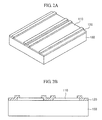
- FIGS. 1A and 2A are schematic perspective views illustrating a method for manufacturing a transparent electrode pattern
- FIGS. 1B and 2B are sectional views illustrating a method for manufacturing a transparent electrode pattern.
- a transparent electrode 110 is formed on a light-transmissive substrate 100 .
- the light-transmissive substrate 100 may employ a glass or plastic substrate, but is not limited thereto.
- a thin silicon substrate or sapphire substrate may also be used for the light-transmissive substrate 100 .
- a glass substrate is used as the light-transmissive substrate 100 .
- a transparent electrode 110 is formed on the light-transmissive substrate 100 through a sputtering process, but the forming process of the transparent electrode 110 is not limited to the sputtering process.
- the transparent electrode 110 may be formed through various deposition processes besides the sputtering process according to the transparent electrode 110 .
- a conductive thin film having light transmittance of 50% or higher is used for the transparent electrode 110 .
- the conductive thin film may include one of indium tin oxide (ITO), indium zinc oxide (IZO), zinc oxide (ZnO), tin oxide (SnO) and indium oxide (In 2 O 3 ).
- ITO indium tin oxide
- IZO indium zinc oxide
- ZnO zinc oxide
- SnO tin oxide
- In 2 O 3 indium oxide
- ITO is used for the transparent electrode 110 . Therefore, an ITO layer is formed on a glass substrate through a sputtering process and the transparent electrode 110 is then formed.
- the transparent electrode 110 is patterned by removing a portion of the transparent electrode 110 using a laser 200 . That is, the transparent electrode 110 is left remaining on an active region (for example, a region where an electro-optic device will be formed) through a laser scribing process, whereas the transparent electrode 110 of an inactive region is removed.
- the transparent electrode 110 is patterned by irradiating a laser beam in one direction.
- the transparent electrode 110 can be formed in a line shape, not a plate shape, on the light-transmissive substrate 100 by patterning the transparent electrode through the laser scribing process, so that power can be uniformly supplied to the entire transparent electrode 110 .
- an edge portion of the patterned transparent electrode 110 is deformed due to high heat or energy produced during process. This may cause the reliability of the device to be deteriorated if an electro-optic device pattern is formed in the edge region of the transparent electrode 110 .
- an insulating protective layer 120 is formed in the edge region of the patterned transparent electrode 110 and the substrate 110 from which the transparent electrode 110 is removed.
- the insulating protective layer 120 may be formed through a printing process. Through the printing process, the insulating protective layer 120 can be selectively formed in the edge region of the transparent electrode 110 .
- a screen printing process is used as the printing process.
- a stencil mask exposing the edge region of the transparent electrode 110 is disposed on the substrate 100 .
- an insulating coating material is applied on the stencil mask.
- the edge region of the transparent electrode 110 exposed by an opening of the stencil mask is coated with the insulating coating material by spreading the coating material on the stencil mask using the squeeze.
- the active region that is, a central region of the patterned transparent electrode 110
- the stencil mask is removed and then heat is applied or light is irradiated to cure the insulating coating material.
- the insulating protective layer 120 is formed. Heat may be applied or light may be irradiated differently according to the insulating coating material.
- the insulating coating material may include an organic material such as photoresist (PR) or an inorganic material such as piezoelectric ceramic (PZT), alumina (Al 2 O 3 ), oxide, nitride and the like.
- the insulating coating material may have fluidity. Accordingly, phase of the insulating coating material may be one of liquid, gel, and paste.
- the insulating coating material may include a photocurable or thermosetting material.
- the transparent electrode 110 is patterned in a line shape.
- the transparent electrode 110 is patterned through the laser scribing process, and the edge region of the patterned transparent electrode 110 is protected through the screen printing process, thus making it possible to simplify a manufacturing process compared to the related art manufacturing process of forming the insulating protective layer through a photolithography process.
- manufacturing facilities can be simplified because only a screen printing apparatus, a heating or light irradiating apparatus, and a cleaning process are used to form the insulating protective layer 120 in the edge region of the patterned transparent electrode 110 .
- the pattern of the transparent electrode 110 of which the edge region is protected by the insulating protective layer 120 is not limited to the aforesaid shape, but may have various modifications.
- the insulating protective layer 120 may be locally formed only in the edge region of the pattern of the transparent electrode 110 , thus reducing the amount of material to be used. Furthermore, when several electro-optic devices are formed on a single substrate, the electro-optic devices are separated by cutting them along the inactive region. In this case, the cutting process may be more easily performed because the insulating protective layer 120 is not provided in a central region of the inactive region.
- the pattern of the transparent electrode 110 may be formed in the shape of an island, not a straight line, which is illustrated in another modification of FIGS. 4 and 5 .
- a pattern of the transparent electrode 110 is formed in the shape or a rectangular island.
- the transparent electrode 110 is formed on the light-transmissive substrate 100 , and thereafter, the island-like transparent electrode 110 is formed through the laser scribing process.
- the island-like transparent electrode 110 may be formed in such a way that the transparent electrode 110 is primarily patterned by moving the laser in a horizontal direction, and is then secondarily patterned by moving the laser in a vertical direction.
- a pattern of the island-like transparent electrode 110 is variously changed depending on the shape of the active region. That is, the pattern of the transparent electrode 110 may have the shape of a polygonal island, a circular island, or an elliptical island as well as the rectangular island.
- the insulating protective layer 120 is formed in the edge region of the transparent electrode 110 and the inactive region through the printing process.
- this exemplary embodiment is not limited to the above-described process, but the insulating protective layer 120 may be formed by printing the substrate 100 with an insulation ink.
- the transparent electrode 110 may be patterned using a photolithography process and an etching process as well as the laser scribing process. That is, a photoresist mask pattern is formed on the transparent electrode 110 through the photolithography process. The photoresist mask pattern formed on the transparent electrode 110 exposes the transparent electrode 110 of the inactive region. Thereafter, the exposed transparent electrode 110 is removed through an etching process using the photoresist mask pattern as an etch mask. Subsequently, the transparent electrode 110 is patterned by removing the remaining photoresist mask pattern.
- the etching process may be a wet etch or dry etch.
- FIGS. 6( a ) through 6 ( c ) are sectional views illustrating a method for manufacturing an organic light emitting device in accordance with an exemplary embodiment.
- a transparent conductive material is deposited on a light-transmissive substrate 1000 , and then patterned to form a bottom transparent electrode 1100 through a laser scribing process.
- An insulating protective layer 1200 is formed in an edge region of the bottom transparent electrode 1100 through a printing process.
- an organic emitting layer 1300 is formed on the bottom transparent electrode 1100 .
- HIL hole injection layer
- HTL hole transport layer
- EML electron transport layer
- ETL electron injection layer
- the hole injection layer 1310 is obtained by forming an organic layer, e.g., CuPc or MTDATA, on the bottom transparent electrode 1100 .
- the hole transport layer 1320 is obtained by forming an organic layer such as NPB and TPD on the hole injection layer 1310 .
- the emitting layer 1330 is formed on the hole transport layer 1320 .
- the emitting layer 1330 may be one of a green emitting layer including Alq 3 or Alq 3 :C545T, a red emitting layer including Alq 3 :DCJTB, a blue emitting layer including SAlq or DPVBi, and combinations thereof.
- the electron transport layer 1340 is obtained by forming a material layer such as Alq 3 on the emitting layer 1330 .
- the organic emitting layer 1300 may be formed by forming a material layer such as LiF, BCP:Cs or the like on the electron transport layer 1340 .
- a top electrode 1400 is formed on the organic emitting layer 1300 .
- the top electrode 1400 is formed by depositing a metallic material on the organic emitting layer 1300 through a sputtering process.
- the metallic material may include one selected from the group consisting of aluminum (Al), silver (Ag), copper (Cu) and an alloy including at least one of the foregoings, but is not limited thereto.
- a transparent electrode may be used as the top electrode 1400 .
- the technology of the present invention is not limited to the aforesaid electro-optic device where the edge region of the transparent electrode is protected by the insulating protective layer that is formed through the printing process, but may also be applicable to various electro-optic devices.
- the present invention can be variously applied depending on an electro-optic device (i.e., organic emitting layer, light conversion layer) formed on the transparent electrode.
- the present invention may be applicable to various kinds of electro-optic devices such as an optical sensor, a solar cell and a light-emitting diode.
- an insulating protective layer is formed in an edge region of a patterned transparent electrode through a printing process so that an apparatus and method for manufacturing the insulating protective layer can be simplified, resulting in a decrease in manufacturing cost.
Landscapes
- Engineering & Computer Science (AREA)
- Manufacturing & Machinery (AREA)
- Physics & Mathematics (AREA)
- Optics & Photonics (AREA)
- Electroluminescent Light Sources (AREA)
Abstract
Description
Claims (23)
Priority Applications (1)
| Application Number | Priority Date | Filing Date | Title |
|---|---|---|---|
| US13/225,525 US20110315432A1 (en) | 2007-12-31 | 2011-09-05 | Method for manufacturing transparent electrode pattern and method for manufacturing electro-optic device having the transparent electrode pattern |
Applications Claiming Priority (2)
| Application Number | Priority Date | Filing Date | Title |
|---|---|---|---|
| KR1020070141272A KR100986024B1 (en) | 2007-12-31 | 2007-12-31 | Method for manufacturing transparent electrode pattern and method for manufacturing electro-optical device having same |
| KR10-2007-0141272 | 2007-12-31 |
Related Child Applications (1)
| Application Number | Title | Priority Date | Filing Date |
|---|---|---|---|
| US13/225,525 Division US20110315432A1 (en) | 2007-12-31 | 2011-09-05 | Method for manufacturing transparent electrode pattern and method for manufacturing electro-optic device having the transparent electrode pattern |
Publications (2)
| Publication Number | Publication Date |
|---|---|
| US20090170036A1 US20090170036A1 (en) | 2009-07-02 |
| US8062834B2 true US8062834B2 (en) | 2011-11-22 |
Family
ID=40798887
Family Applications (2)
| Application Number | Title | Priority Date | Filing Date |
|---|---|---|---|
| US12/344,488 Active 2030-01-29 US8062834B2 (en) | 2007-12-31 | 2008-12-27 | Method for manufacturing transparent electrode pattern and method for manufacturing electro-optic device having the transparent electrode pattern |
| US13/225,525 Abandoned US20110315432A1 (en) | 2007-12-31 | 2011-09-05 | Method for manufacturing transparent electrode pattern and method for manufacturing electro-optic device having the transparent electrode pattern |
Family Applications After (1)
| Application Number | Title | Priority Date | Filing Date |
|---|---|---|---|
| US13/225,525 Abandoned US20110315432A1 (en) | 2007-12-31 | 2011-09-05 | Method for manufacturing transparent electrode pattern and method for manufacturing electro-optic device having the transparent electrode pattern |
Country Status (3)
| Country | Link |
|---|---|
| US (2) | US8062834B2 (en) |
| KR (1) | KR100986024B1 (en) |
| CN (1) | CN101478032A (en) |
Cited By (4)
| Publication number | Priority date | Publication date | Assignee | Title |
|---|---|---|---|---|
| US20110012094A1 (en) * | 2009-07-15 | 2011-01-20 | Hyung Sup Lee | Electro-Optic Device and Method for Manufacturing the same |
| US20110315432A1 (en) * | 2007-12-31 | 2011-12-29 | Ads | Method for manufacturing transparent electrode pattern and method for manufacturing electro-optic device having the transparent electrode pattern |
| US20120006389A1 (en) * | 2009-06-29 | 2012-01-12 | Kyocera Corporation | Method of Manufacturing Photoelectric Conversion Device, Apparatus for Manufacturing Photoelectric Conversion Device, and Photoelectric Conversion Device |
| US20160034083A1 (en) * | 2014-07-29 | 2016-02-04 | Ibis Innotech Inc. | Touch sensing device |
Families Citing this family (5)
| Publication number | Priority date | Publication date | Assignee | Title |
|---|---|---|---|---|
| JP5478147B2 (en) * | 2009-08-19 | 2014-04-23 | リンテック株式会社 | Luminescent sheet and manufacturing method thereof |
| CN104177130A (en) * | 2013-05-23 | 2014-12-03 | 比亚迪股份有限公司 | Insulating substrate surface patterning method and ceramic |
| JP2017182877A (en) * | 2014-08-19 | 2017-10-05 | パナソニックIpマネジメント株式会社 | Organic electroluminescence device and method for producing transparent electrode plate |
| CN113012846B (en) * | 2019-12-20 | 2024-03-26 | 荣耀终端有限公司 | Conductive electrode, preparation method thereof and electronic equipment |
| CN112428700A (en) * | 2020-11-11 | 2021-03-02 | 大连理工大学 | Integrated ink-jet printing manufacturing device and method for flexible bendable OLED screen |
Citations (6)
| Publication number | Priority date | Publication date | Assignee | Title |
|---|---|---|---|---|
| JPS6397922A (en) | 1986-10-14 | 1988-04-28 | Hitachi Maxell Ltd | Production of electrochromic display element |
| JPH01246877A (en) | 1988-03-28 | 1989-10-02 | Kyocera Corp | Photoelectric conversion device |
| US5737049A (en) * | 1995-05-09 | 1998-04-07 | Lg Electronics, Inc. | Liquid crystal display device having storage capacitors of increased capacitance and fabrication method therefor |
| US6445428B1 (en) * | 1998-05-28 | 2002-09-03 | Fujitsu Limited | Thin film transistor for a liquid crystal display device and a fabrication process thereof |
| KR20060049490A (en) | 2004-06-21 | 2006-05-19 | 삼성전자주식회사 | Organic insulating film composition and pattern forming method of organic insulating film using the same |
| US20080124522A1 (en) * | 2004-10-25 | 2008-05-29 | Takashi Chuman | Electronic Circuit Board and its Manufacturing Method |
Family Cites Families (1)
| Publication number | Priority date | Publication date | Assignee | Title |
|---|---|---|---|---|
| KR100986024B1 (en) * | 2007-12-31 | 2010-10-07 | (주)에이디에스 | Method for manufacturing transparent electrode pattern and method for manufacturing electro-optical device having same |
-
2007
- 2007-12-31 KR KR1020070141272A patent/KR100986024B1/en not_active Expired - Fee Related
-
2008
- 2008-12-27 US US12/344,488 patent/US8062834B2/en active Active
- 2008-12-30 CN CNA2008101873758A patent/CN101478032A/en active Pending
-
2011
- 2011-09-05 US US13/225,525 patent/US20110315432A1/en not_active Abandoned
Patent Citations (7)
| Publication number | Priority date | Publication date | Assignee | Title |
|---|---|---|---|---|
| JPS6397922A (en) | 1986-10-14 | 1988-04-28 | Hitachi Maxell Ltd | Production of electrochromic display element |
| JPH01246877A (en) | 1988-03-28 | 1989-10-02 | Kyocera Corp | Photoelectric conversion device |
| US5737049A (en) * | 1995-05-09 | 1998-04-07 | Lg Electronics, Inc. | Liquid crystal display device having storage capacitors of increased capacitance and fabrication method therefor |
| US6445428B1 (en) * | 1998-05-28 | 2002-09-03 | Fujitsu Limited | Thin film transistor for a liquid crystal display device and a fabrication process thereof |
| KR20060049490A (en) | 2004-06-21 | 2006-05-19 | 삼성전자주식회사 | Organic insulating film composition and pattern forming method of organic insulating film using the same |
| US20080124522A1 (en) * | 2004-10-25 | 2008-05-29 | Takashi Chuman | Electronic Circuit Board and its Manufacturing Method |
| US7968458B2 (en) * | 2004-10-25 | 2011-06-28 | Pioneer Corporation | Electronic circuit board and its manufacturing method |
Cited By (6)
| Publication number | Priority date | Publication date | Assignee | Title |
|---|---|---|---|---|
| US20110315432A1 (en) * | 2007-12-31 | 2011-12-29 | Ads | Method for manufacturing transparent electrode pattern and method for manufacturing electro-optic device having the transparent electrode pattern |
| US20120006389A1 (en) * | 2009-06-29 | 2012-01-12 | Kyocera Corporation | Method of Manufacturing Photoelectric Conversion Device, Apparatus for Manufacturing Photoelectric Conversion Device, and Photoelectric Conversion Device |
| US20110012094A1 (en) * | 2009-07-15 | 2011-01-20 | Hyung Sup Lee | Electro-Optic Device and Method for Manufacturing the same |
| US8399276B2 (en) * | 2009-07-15 | 2013-03-19 | Jusung Engineering Co., Ltd. | Electro-optic device and method for manufacturing the same |
| US9000454B2 (en) | 2009-07-15 | 2015-04-07 | Jusung Engineering Co., Ltd. | Electro-optic device and method for manufacturing the same |
| US20160034083A1 (en) * | 2014-07-29 | 2016-02-04 | Ibis Innotech Inc. | Touch sensing device |
Also Published As
| Publication number | Publication date |
|---|---|
| KR100986024B1 (en) | 2010-10-07 |
| US20110315432A1 (en) | 2011-12-29 |
| KR20090073352A (en) | 2009-07-03 |
| CN101478032A (en) | 2009-07-08 |
| US20090170036A1 (en) | 2009-07-02 |
Similar Documents
| Publication | Publication Date | Title |
|---|---|---|
| US8062834B2 (en) | Method for manufacturing transparent electrode pattern and method for manufacturing electro-optic device having the transparent electrode pattern | |
| JP6154572B2 (en) | Mask frame assembly for thin film deposition | |
| US6949389B2 (en) | Encapsulation for organic light emitting diodes devices | |
| JP4520708B2 (en) | Method and electronic device for encapsulating a plurality of devices fabricated on a substrate | |
| TW201240077A (en) | Method of manufacturing organic electroluminescence display device | |
| KR101483193B1 (en) | Method for manufacturing thin film pattern and optical device using the same | |
| US9281492B2 (en) | Electro-optic device and method for manufacturing same | |
| KR20160049610A (en) | Optical patterning mask and fabricating of display device using the same | |
| US20090294157A1 (en) | Electro-optic device and method for manufacturing the same | |
| US9000454B2 (en) | Electro-optic device and method for manufacturing the same | |
| KR20030075971A (en) | Method for fabricating thin film pattern for organic electronic devices | |
| KR101236427B1 (en) | Method of manufacturing gate insulator and thin film transistor adopting the insulator | |
| EP1796184B1 (en) | Organic thin film transistor, method of manufacturing the same, and organic light emitting display device having the same | |
| JP2020042115A (en) | Display panel manufacturing apparatus and display panel manufacturing method | |
| CN110931535B (en) | Micro OLED structure and preparation method thereof | |
| KR102577783B1 (en) | Method for manufacturing optoelectronic device | |
| KR20100022627A (en) | Method for manufacturing electro-optic device | |
| EP2784840B1 (en) | Method of manufacturing an organic device | |
| KR100623704B1 (en) | Manufacturing Method of Organic Electroluminescent Display | |
| KR100700656B1 (en) | Organic electroluminescent device and manufacturing method thereof | |
| TW202602333A (en) | Overhang pattern for advanced oled patterning | |
| US20190115539A1 (en) | Organic light emitting diode structure and method for manufacturing the same | |
| KR20020057024A (en) | Method for forming sidewall of organic electro-luminescent display |
Legal Events
| Date | Code | Title | Description |
|---|---|---|---|
| AS | Assignment |
Owner name: ADS, KOREA, DEMOCRATIC PEOPLE'S REPUBLIC OF Free format text: ASSIGNMENT OF ASSIGNORS INTEREST;ASSIGNORS:LEE, HYUNG SUP;LEE, KYOO HWAN;KWON, YOUNG HO;REEL/FRAME:022031/0991 Effective date: 20081219 Owner name: JUSUNG ENGNINEERING CO., LTD., KOREA, DEMOCRATIC P Free format text: ASSIGNMENT OF ASSIGNORS INTEREST;ASSIGNORS:LEE, HYUNG SUP;LEE, KYOO HWAN;KWON, YOUNG HO;REEL/FRAME:022031/0991 Effective date: 20081219 |
|
| STCF | Information on status: patent grant |
Free format text: PATENTED CASE |
|
| FEPP | Fee payment procedure |
Free format text: PAYOR NUMBER ASSIGNED (ORIGINAL EVENT CODE: ASPN); ENTITY STATUS OF PATENT OWNER: SMALL ENTITY |
|
| FEPP | Fee payment procedure |
Free format text: PAT HOLDER CLAIMS SMALL ENTITY STATUS, ENTITY STATUS SET TO SMALL (ORIGINAL EVENT CODE: LTOS); ENTITY STATUS OF PATENT OWNER: SMALL ENTITY |
|
| FPAY | Fee payment |
Year of fee payment: 4 |
|
| MAFP | Maintenance fee payment |
Free format text: PAYMENT OF MAINTENANCE FEE, 8TH YR, SMALL ENTITY (ORIGINAL EVENT CODE: M2552); ENTITY STATUS OF PATENT OWNER: SMALL ENTITY Year of fee payment: 8 |
|
| AS | Assignment |
Owner name: ADS, KOREA, REPUBLIC OF Free format text: CORRECTIVE ASSIGNMENT TO CORRECT THE COUNTRY NAME IN THE ASSIGNEE'S ADDRESS PREVIOUSLY RECORDED AT REEL: 022031 FRAME: 0991. ASSIGNOR(S) HEREBY CONFIRMS THE ASSIGNMENT;ASSIGNORS:LEE, HYUNG SUP;LEE, KYOO HWAN;KWON, YOUNG HO;REEL/FRAME:060130/0684 Effective date: 20081219 Owner name: JUSUNG ENGINEERING CO., LTD., KOREA, REPUBLIC OF Free format text: CORRECTIVE ASSIGNMENT TO CORRECT THE COUNTRY NAME IN THE ASSIGNEE'S ADDRESS PREVIOUSLY RECORDED AT REEL: 022031 FRAME: 0991. ASSIGNOR(S) HEREBY CONFIRMS THE ASSIGNMENT;ASSIGNORS:LEE, HYUNG SUP;LEE, KYOO HWAN;KWON, YOUNG HO;REEL/FRAME:060130/0684 Effective date: 20081219 |
|
| FEPP | Fee payment procedure |
Free format text: ENTITY STATUS SET TO UNDISCOUNTED (ORIGINAL EVENT CODE: BIG.); ENTITY STATUS OF PATENT OWNER: LARGE ENTITY |
|
| MAFP | Maintenance fee payment |
Free format text: PAYMENT OF MAINTENANCE FEE, 12TH YEAR, LARGE ENTITY (ORIGINAL EVENT CODE: M1553); ENTITY STATUS OF PATENT OWNER: LARGE ENTITY Year of fee payment: 12 |