US8059677B1 - Scalable channel bundling with adaptable channel synchronization - Google Patents
Scalable channel bundling with adaptable channel synchronization Download PDFInfo
- Publication number
- US8059677B1 US8059677B1 US12/427,960 US42796009A US8059677B1 US 8059677 B1 US8059677 B1 US 8059677B1 US 42796009 A US42796009 A US 42796009A US 8059677 B1 US8059677 B1 US 8059677B1
- Authority
- US
- United States
- Prior art keywords
- signal
- bundle
- data channel
- distribution circuitry
- master
- Prior art date
- Legal status (The legal status is an assumption and is not a legal conclusion. Google has not performed a legal analysis and makes no representation as to the accuracy of the status listed.)
- Active, expires
Links
Images


Classifications
-
- G—PHYSICS
- G06—COMPUTING OR CALCULATING; COUNTING
- G06F—ELECTRIC DIGITAL DATA PROCESSING
- G06F30/00—Computer-aided design [CAD]
- G06F30/30—Circuit design
- G06F30/32—Circuit design at the digital level
- G06F30/327—Logic synthesis; Behaviour synthesis, e.g. mapping logic, HDL to netlist, high-level language to RTL or netlist
Definitions
- This invention relates generally to the area of system interconnect technology.
- integrated circuit (IC) devices increasingly need to support high speed serial interface (“HSSI”) protocols
- HSSI high speed serial interface
- PCS physical coding sub-layer
- Successfully bundling these channels requires synchronizing clock signals and control signals across multiple channels.
- HSSI protocols evolve, there is an increasing need to be able to bundle an arbitrarily large number of data channels.
- a scalable solution that allows for bundling (sometimes called “bonding”) a large number of channels is needed.
- signal distribution circuitry includes a data path with registers coupled to adjacent sets of data channels in a bundle of data channel sets.
- self-switch circuits allow data channels in a bundle of data channel sets to switch from bundle-wide signals to locally generated signals after the bundle-wide signals have been synchronously distributed to all channel sets in the bundle.
- signal distribution circuitry is used to distribute a divided clock signal.
- signal distribution circuitry is used to distribute enable signals for first-in first-out circuits (“FIFOs”) located in channels of each data channel set in channel set bundle. In a particular aspect, FIFO read and write operations across a channel set bundle are initiated such that a difference between read and write pointer values is the same in each channel set.
- FIFOs first-in first-out circuits
- FIG. 1 illustrates signal distribution circuitry in accordance with an embodiment of the present invention implemented in data channel bundle.
- FIG. 2 shows further details of the self switch circuits and local clock circuits of the embodiment of FIG. 1 .
- FIG. 3 is a timing diagram illustrating timing for the distribution of certain signals generated in the embodiment illustrated in FIGS. 1 and 2 .
- FIG. 4 illustrates signal distribution circuitry in accordance with another embodiment of the present invention implemented in a data channel bundle.
- FIG. 5 shows further details of the self switch circuits and local enable generator circuits of the embodiment of FIG. 4 .
- FIG. 6 is a timing diagram that further illustrates the operating principles of the embodiment illustrated in FIGS. 4 and 5 .
- FIG. 7 illustrates an exemplary data processing system including a transceiver in a programmable logic device (“PLD”), the transceiver including circuitry in accordance with an embodiment of the present invention.
- PLD programmable logic device
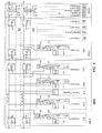
- FIG. 1 illustrates signal distribution circuitry in accordance with an embodiment of the present invention implemented in data channel bundle 1000 .
- the term “data channel” as used herein simply refers to a collection of circuitry that receives and/or transmits a high speed data stream.
- Bundle 1000 comprises a plurality of sets of data channels including data channel sets 100 - 1 , 100 - 2 , and 100 - 3 .
- Data channel set 100 - 1 comprises four data channels including channels 110 , 111 , 113 , and 114 .
- data channel set 100 - 1 is referred to as a “quad” because it has four data channels. However, in other embodiments, a set of data channels may have more or few data channels.
- Data channel set 100 - 1 further comprises central channel 112 .
- Central channel 112 includes circuitry for generating various control and/or clock signals used by other data channels in sets 100 - 1 , 100 - 2 , and 100 - 3 .
- Data channel set 100 - 2 also comprises four data channels including channels 120 , 121 , 123 , and 124 as well as a central channel 122 .
- data channel set 100 - 3 comprises four data channels including channels 130 , 131 , 133 , and 134 as well as a central channel 132 .
- quad 100 - 1 is designated as the “master” quad and quads 100 - 2 and 100 - 3 are “slave” quads.
- Master and slave in this context simply refer to the fact that the relevant clock signal and control signals used by the entire bundle are synchronized to signals from the master quad 100 - 1 .
- master signal will be used herein simply as a label to indicate a signal distributed from one quad to other quads as distinguished from a “local” signal generated and used locally in a channel.
- Clock divider circuitry in central channel 112 comprises register 191 and inverter 192 coupled together as shown.
- Full speed clock signal CLK (lower case letters used in the drawing) is received at a clock input of register 191 and is used to generate divided clock signal CLK/2 which has a frequency that is half the frequency of full speed clock signal CLK.
- CLK/2 is delivered to a first input of a multiplexor (“mux”) 103 in each of data channels 110 , 111 , 113 , and 114 .
- Each mux 103 is controlled by a self-switch circuit 102 .
- the output of each mux 103 is coupled to a local clock circuit 101 which also receives full speed clock signal CLK.
- a second input of each mux 103 is coupled to receive output from local clock circuit 101 .
- Data channels 120 , 121 , 123 , and 124 in data channel set 100 - 2 and data channels 130 , 131 , 133 , and 134 in data channel set 100 - 3 each also include a self-switch circuit 102 , a mux 103 , and a local clock circuit 101 , all coupled as shown. This circuitry is present but not separately shown for data channels in channel set 100 - 3 to avoid over-crowding the drawing.
- the master quad is shown on the left and drives the relevant signal in one direction to consecutive quads from left to right.
- the illustrated embodiment could readily be modified to make a different quad (e.g. 100 - 2 or 100 - 3 ) the master quad instead.
- the master quad may drive signals in different directions to slave quads on different sides of the master quad (for example, the illustrated embodiment could be re-designed such that channel set 100 - 2 serve as the master quad and channel sets 100 - 1 and 100 - 3 serve as slave quads).
- Channel set bundle 1000 includes bundle-wide distribution circuitry 150 including two registers 151 coupled to adjacent channel sets, lines coupled to the data channels in each channel set ( 100 - 1 , 100 - 2 , and 100 - 3 ), and a line coupled to receive output from central channel 112 in channel set 100 - 1 .
- FIG. 2 shows further details of the self switch circuits 102 and local clock circuits 101 of the embodiment of FIG. 1 .
- Local clock circuit 101 comprises register 101 - 1 and inverter 101 - 2 coupled as shown.
- Self switch circuit 102 comprises N-bit counter 102 - 1 , AND gate 102 - 3 , and inverter 102 - 2 , all coupled as shown.
- Self switch circuit 102 is coupled to a control input of mux 103 . Initially, the output signal SS of self switch circuit 102 is low and therefore input “0” of mux 103 is selected. Therefore, register 101 - 1 in local clock circuitry 101 receives a divided clock signal from bundle-wide distribution circuitry 150 .
- N-bit counter 102 - 1 counts rising edges of full speed clock signal CLK.
- N-bit counter 102 - 1 After a pre-determined count is reached, the output of N-bit counter 102 - 1 becomes such that N high signals are provided to AND gate 102 - 3 , thus switching the self switch circuit 102 's output signal SS from low to high. This switches the control signal for mux 103 so that mux 103 switches to select its “1” input.
- divided clock signal CLK/2 Prior to the switch, divided clock signal CLK/2 is provided to the channel from bundle-wide distribution circuitry 150 via register 101 - 1 .
- register 101 - 1 in conjunction with inverter 101 - 2 acts as a clock divider adapted to divide full speed clock signal CLK and provide a divided clock locally without the channel having to continue receiving a master divided clock from bundle-wide distribution circuitry 150 .
- the timing for distributing a “master” divided clock CLK/2 from quad 100 - 1 is such that it reaches destination circuitry in the channels of the furthest quad (quad 100 - 3 ) on the fourth rising edge of full speed clock signal CLK.
- FIG. 3 is a timing diagram illustrating timing for the distribution of master divided clock signal CLK/2 from central channel 112 in master quad 100 - 1 to channels in slave quads 100 - 2 and 100 - 3 .
- the points of distribution to destination circuitry in the data channels of quads 100 - 1 , 100 - 2 , and 100 - 3 are, respectively C, E, and G.
- signal CLK/2 is synchronous at its destination points in the data channels of all three quads 100 - 1 , 100 - 2 , and 100 - 3 .
- FIG. 4 illustrates signal distribution circuitry in accordance with another embodiment of the present invention implemented in data channel bundle 4000 .
- the embodiments of FIG. 1 and FIG. 4 may be implemented together in the same data channel bundle.
- bundle 4000 (in addition to bundle 1000 ) is only for purposes of easier illustration and explanation.
- the embodiment of FIG. 4 illustrates use of the principles of the present invention to synchronously distribute control signals.
- the control signals are read and write enable signals for first-in first-out circuits (“FIFOs”) that reside in each data channel as will be further described below.
- Bundle 4000 comprises a plurality of sets of data channels including data channel set 400 - 1 , 400 - 2 , and 400 - 3 .
- Data channel set 400 - 1 comprises four data channels including channels 410 , 411 , 413 , and 414 , and in this particular example, may also be referred to as a “quad.”
- Data channel set 400 - 1 further comprises central channel 412 used to generate various control and/or clock signals used by data channels in channel sets 400 - 1 , 400 - 2 , and 400 - 3 .
- Data channel set 400 - 2 also comprises four data channels including channels 420 , 421 , 423 , and 424 as well as a central channel 422 .
- data channel set 400 - 3 comprises four data channels including channels 430 , 431 , 433 , and 434 as well as a central channel 432 .
- quad 400 - 1 is designated as the “master” quad and quads 400 - 2 and 400 - 3 are “slave” quads.
- Central channel 412 includes enable signal generator 412 - 1 for generating master write enable signal wr_en_M and master read enable signal rd_en_M.
- enable signal generator 412 - 1 can, in a particular example, include circuitry similar to that of the local enable signal circuits 401 further described in the context of FIG. 5 .
- Each data channel comprises a FIFO 407 , a mux 403 , a mux 404 , a self switch circuit 402 , and a local enable signal generator circuit 401 .
- Signal wr_en_M is delivered to a first input of a mux 403 in each of data channels 410 , 411 , 413 , and 414 .
- Signal rd_enable_M is delivered to a first input of a mux 404 in each of data channels 410 , 411 , 413 , and 414 .
- Each mux 403 and 404 is controlled by a self-switch circuit 402 .
- the output of each mux 403 and 404 is coupled to a FIFO 407 .
- a second input of each mux 103 is coupled to receive output from a local enable signal circuit 401 .
- Data channels 420 , 421 , 423 , and 424 in data channel set 400 - 2 and data channels 430 , 431 , 433 , and 434 in data channel set 400 - 3 each include a FIFO 407 , a mux 403 , a mux 404 , a self switch circuit 402 , and a local enable signal generator circuit 401 .
- This circuitry is shown in data channel 420 of data channel set 400 - 2 and is present but not separately shown for the other data channels in data channel sets 400 - 2 and 400 - 3 to avoid over-crowding the drawing.
- Channel set bundle 4000 includes bundle-wide write enable distribution circuitry 450 including two registers 451 coupled to adjacent channel sets, lines coupled to the data channels in each channel set ( 400 - 1 , 400 - 2 , and 400 - 3 ), and a line coupled to receive output (wr_en_M) from enable signal generator 412 - 1 in central channel 412 of channel set 400 - 1 .
- Channel set bundle 4000 also includes bundle-wide read enable distribution circuitry 460 including two registers 461 coupled across each channel set, lines coupled to the data channels in each channel set ( 400 - 1 , 400 - 2 , and 400 - 3 ), and a line coupled to receive output (rd_en_M) from enable signal generator 412 - 1 in central channel 412 of channel set 400 - 1 .
- bundle-wide read enable distribution circuitry 460 including two registers 461 coupled across each channel set, lines coupled to the data channels in each channel set ( 400 - 1 , 400 - 2 , and 400 - 3 ), and a line coupled to receive output (rd_en_M) from enable signal generator 412 - 1 in central channel 412 of channel set 400 - 1 .
- FIG. 5 shows further details of the self switch circuits 402 and local enable generator circuits 401 of the embodiment of FIG. 4 .
- Local enable generator circuit 401 provides a “high” local enable signal to write enable timing register 401 - w and to read enable timing register 401 - r .
- Self-switch circuit 402 comprises N-bit counter 402 - 1 , AND gate 402 - 3 , and inverter 402 - 2 , all coupled as shown.
- Self switch circuit 402 is coupled to control inputs of muxes 403 and 404 . Initially, the output of self switch circuit 402 is low and therefore the “0” inputs of muxes 403 and 404 are selected.
- timing register 408 - w receives master write enable signal wr_en_M from bundle-wide write enable distribution circuitry 450 and timing register 408 - r receives master read enable signal rd_en_M from bundle-wide read enable distribution circuitry 460 .
- the outputs of N-bit counter 402 - 1 are such that N high signals are provided to AND gate 402 - 3 , thus switching the output of self-switch circuit 402 from low to high. This switches the control signal for muxes 403 and 404 from low to high so each mux switches to select its “1” input.
- timing registers 408 - w and 408 - r receive, respectively, local write enable signal wr_en_L and local read enable signal rd_en_L from local enable signal circuit 401 .
- the timing for distributing “master” read and write enable signals from quad 400 - 1 is such that the master write enable signal wr_en_M and the master read enable signal rd_en_M reach destination circuitry in the channels of the furthest quad (quad 400 - 3 ) after seven clock cycles. Therefore, in the present example, N-bit counter 402 - 1 is a 3-bit counter (which counts eight clock cycles before switching from low to high) which allows sufficient time for master enable signals to be delivered to all quads before switching each channel to a local enable signal.
- FIFO 407 has write control circuitry 407 - w and read control circuitry 407 - r .
- write control circuitry 407 - w begins generating a 3-bit write pointer signal wr_p whose value corresponds to a particular location in the FIFO memory.
- read control circuitry 407 - r begins generating a 3-bit read pointer signal rd_p whose value corresponds to a particular location in the FIFO memory.
- FIFO 407 is an 8-bit circular asynchronous FIFO.
- the write clock signal clk-w and the read clock signal ckl-r are the same frequency but have slightly different phases (as illustrated in FIG. 6 ).
- the write pointer wr_p has value of “2” on the first clock cycle, which identifies the “2” location of FIFO 407 's memory.
- the write pointer advances one value to point to a different location of FIFO 407 's memory.
- the write pointer reaches the “7” location in memory, it returns on the next clock cycle to “0” and begins circling through each memory location again.
- the read pointer signal generated by read control circuitry 407 - r proceeds in similar fashion. However, FIFO 407 is designed such that, when first enabled (or “reset”), the read pointer rd_p points to memory location “0” (in contrast to the write pointer, which points to location “2”).
- the illustrated embodiment operates on the principle that for circular FIFOs operate in coordinated fashion across multiple quads, it is not necessary for a read (or write) pointer in one quad to simultaneously have the same value as a read (or write) pointer in a second quad. However, to have the same latency through FIFOs in the different channels across multiple quads, it is necessary that the difference in values between the read and write pointers in each quad is the same.
- FIG. 6 is a timing diagram that further illustrates the operating principles of the embodiment illustrated in FIGS. 4 and 5 .
- the timing of the write and read enable signals is shown with respect to the “A,” “B,” and “C” locations marked in FIG. 4 .
- each location corresponds to an input of a FIFO 407 's control circuitry 407 - w and 407 - r .
- location “A” references input to FIFOs 407 in quad 400 - 1
- location “B” references input to FIFOs 407 in quad 400 - 2
- location “C” references input to FIFOs 407 in quad 400 - 3 .
- write control circuits 407 - w for FIFOs 407 in quad 400 - 1 begin generating a write pointer signal starting with a value of 2 and advance the value once each clock cycle.
- the enable signals switch to local control as described above in the context of FIG. 5 .
- Data channel bundles 1000 in FIG. 1 and/or 4000 in FIG. 4 and associated distribution and self-switch circuitry may be implemented as part of input/out (“I/O”) circuitry—for example, as part of physical coding sub-layer (“PCS”) circuitry in any IC.
- I/O input/out
- PCS physical coding sub-layer
- a specific example of an IC is a programmable logic device (“PLD”).
- PLDs also referred to as complex PLDs, programmable array logic, programmable logic arrays, field PLAs, erasable PLDs, electrically erasable PLDs, logic cell arrays, field programmable gate arrays, or by other names
- PLDs provide the advantages of fixed ICs with the flexibility of custom ICs.
- PLDs have configuration elements (i.e., programmable elements) that may be programmed or reprogrammed. Placing new data into the configuration elements programs or reprograms the PLD's logic functions and associated routing pathways. Such configuration may be accomplished via data stored in programmable elements on the IC. Programmable elements may include dynamic or static RAM, flip-flops, electronically erasable programmable read-only memory (EEPROM) cells, flash, fuse, anti-fuse programmable connections, or other memory elements. Configuration may also be accomplished via one or more externally generated signals received by the IC during operation of the IC. Data represented by such signals may or may not be stored on the IC during operation of the IC. Configuration may also be accomplished via mask programming during fabrication of the IC. While mask programming may have disadvantages relative to some of the field programmable options already listed, it may be useful in certain high volume applications.
- EEPROM electronically erasable programmable read-only memory
- FIG. 7 illustrates an exemplary data processing system 700 including a PLD 710 .
- PLD 710 includes a transceiver 701 with PCS circuitry including channel set bundles in accordance with an embodiment of the present invention.
- PCS circuitry including channel set bundles in accordance with an embodiment of the present invention.
- FIG. 7 illustrates only a single transceiver 701 ; however, a PLD such as PLD 710 may include multiple transceivers 701 .
- Data processing system 700 may include one or more of the following additional components: processor 740 , memory 750 , input/output (I/O) circuitry 720 , and peripheral devices 730 and/or other components. These components are coupled together by system bus 765 and are populated on circuit board 760 which is contained in end-user system 770 .
- a data processing system such as system 700 may include a single end-user system such as end-user system 770 or may include a plurality of systems working together as a data processing system.
- System 700 can be used in a wide variety of applications, such as computer networking, data networking, instrumentation, video processing, digital signal processing, or any other application where the advantage of using programmable or reprogrammable logic in system design is desirable.
- PLD 710 can be used to perform a variety of different logic functions.
- PLD 710 can be configured as a processor or controller that works in cooperation with processor 740 (or, in alternative embodiments, a PLD might itself act as the sole system processor).
- PLD 710 may also be used as an arbiter for arbitrating access to shared resources in system 700 .
- PLD 710 can be configured as an interface between processor 740 and one of the other components in system 700 . It should be noted that system 700 is only exemplary.
- system 700 is a digital system.
- a digital system is not intended to be limited to a purely digital system, but also encompasses hybrid systems that include both digital and analog subsystems.
Landscapes
- Engineering & Computer Science (AREA)
- Computer Hardware Design (AREA)
- Physics & Mathematics (AREA)
- Theoretical Computer Science (AREA)
- Evolutionary Computation (AREA)
- Geometry (AREA)
- General Engineering & Computer Science (AREA)
- General Physics & Mathematics (AREA)
- Logic Circuits (AREA)
Abstract
Description
Claims (26)
Priority Applications (1)
| Application Number | Priority Date | Filing Date | Title |
|---|---|---|---|
| US12/427,960 US8059677B1 (en) | 2009-04-22 | 2009-04-22 | Scalable channel bundling with adaptable channel synchronization |
Applications Claiming Priority (1)
| Application Number | Priority Date | Filing Date | Title |
|---|---|---|---|
| US12/427,960 US8059677B1 (en) | 2009-04-22 | 2009-04-22 | Scalable channel bundling with adaptable channel synchronization |
Publications (1)
| Publication Number | Publication Date |
|---|---|
| US8059677B1 true US8059677B1 (en) | 2011-11-15 |
Family
ID=44906982
Family Applications (1)
| Application Number | Title | Priority Date | Filing Date |
|---|---|---|---|
| US12/427,960 Active 2030-05-12 US8059677B1 (en) | 2009-04-22 | 2009-04-22 | Scalable channel bundling with adaptable channel synchronization |
Country Status (1)
| Country | Link |
|---|---|
| US (1) | US8059677B1 (en) |
Cited By (2)
| Publication number | Priority date | Publication date | Assignee | Title |
|---|---|---|---|---|
| US8812893B1 (en) | 2012-06-01 | 2014-08-19 | Altera Corporation | Apparatus and methods for low-skew channel bonding |
| US20160119069A1 (en) * | 2012-03-11 | 2016-04-28 | Broadcom Corporation | Channel Bonding Synchronization |
Citations (3)
| Publication number | Priority date | Publication date | Assignee | Title |
|---|---|---|---|---|
| US6993671B2 (en) | 2003-03-28 | 2006-01-31 | International Business Machines Corporation | High speed clock divider with synchronous phase start-up over physically distributed space |
| US20070058618A1 (en) | 2005-07-19 | 2007-03-15 | Altera Corporation | Multi-channel communication circuitry for programmable logic device integrated circuits and the like |
| US20090274131A1 (en) * | 2008-04-30 | 2009-11-05 | The Industry & Academic Cooperation In Chungnam National University (Iac) | Method and system for dynamic distribution of traffic in channel bonding wireless local area network(lan) systems |
-
2009
- 2009-04-22 US US12/427,960 patent/US8059677B1/en active Active
Patent Citations (3)
| Publication number | Priority date | Publication date | Assignee | Title |
|---|---|---|---|---|
| US6993671B2 (en) | 2003-03-28 | 2006-01-31 | International Business Machines Corporation | High speed clock divider with synchronous phase start-up over physically distributed space |
| US20070058618A1 (en) | 2005-07-19 | 2007-03-15 | Altera Corporation | Multi-channel communication circuitry for programmable logic device integrated circuits and the like |
| US20090274131A1 (en) * | 2008-04-30 | 2009-11-05 | The Industry & Academic Cooperation In Chungnam National University (Iac) | Method and system for dynamic distribution of traffic in channel bonding wireless local area network(lan) systems |
Non-Patent Citations (1)
| Title |
|---|
| U.S. Appl. No. 11/895,594, filed Aug. 24, 2007, Xue et al. |
Cited By (3)
| Publication number | Priority date | Publication date | Assignee | Title |
|---|---|---|---|---|
| US20160119069A1 (en) * | 2012-03-11 | 2016-04-28 | Broadcom Corporation | Channel Bonding Synchronization |
| US10079727B2 (en) * | 2012-03-11 | 2018-09-18 | Avago Technologies General Ip (Singapore) Pte. Ltd. | Channel bonding synchronization |
| US8812893B1 (en) | 2012-06-01 | 2014-08-19 | Altera Corporation | Apparatus and methods for low-skew channel bonding |
Similar Documents
| Publication | Publication Date | Title |
|---|---|---|
| US6512395B1 (en) | Configurable memory for programmable logic circuits | |
| US7038952B1 (en) | Block RAM with embedded FIFO buffer | |
| US10210914B2 (en) | Programmable logic accelerator in system on chip | |
| US9685957B2 (en) | System reset controller replacing individual asynchronous resets | |
| US20080263334A1 (en) | Dynamically configurable and re-configurable data path | |
| US8516025B2 (en) | Clock driven dynamic datapath chaining | |
| US8248110B1 (en) | Clock switch-over circuits and methods | |
| CN103477562B (en) | Processor and the method for operating processor | |
| CN107743621B (en) | IC input and output | |
| US8059677B1 (en) | Scalable channel bundling with adaptable channel synchronization | |
| US7827433B1 (en) | Time-multiplexed routing for reducing pipelining registers | |
| US6249149B1 (en) | Apparatus and method for centralized generation of an enabled clock signal for a logic array block of a programmable logic device | |
| CN114514513A (en) | N-channel serial peripheral communication, and related systems, methods, and devices | |
| EP1612662A2 (en) | Address generator and arithmetic circuit | |
| US20050289327A1 (en) | Reconfigurable processor and semiconductor device | |
| EP1388048B1 (en) | Storage system for use in custom loop accellerators | |
| US10389341B1 (en) | Synchronize-able modular physical layer architecture for scalable interface | |
| US8504745B1 (en) | Method of and circuit for determining a shift pattern to generate an output data stream | |
| KR20100082834A (en) | Clock circuit with clock transfer capability and method | |
| US7239260B2 (en) | Analog-to-digital interfacing device and method of analog-to-digital interfacing | |
| US8193953B1 (en) | Data width scaler circuitry | |
| TWI559149B (en) | Configurable logic cells | |
| US9558131B1 (en) | Integrated circuit with bonding circuits for bonding memory controllers | |
| CN117792359A (en) | Multiplexing selection circuit of chip external reset pin and chip | |
| US7528642B2 (en) | Semiconductor integrated circuit device and method of outputting signals on semiconductor integrated circuit |
Legal Events
| Date | Code | Title | Description |
|---|---|---|---|
| AS | Assignment |
Owner name: ALTERA CORPORATION, CALIFORNIA Free format text: ASSIGNMENT OF ASSIGNORS INTEREST;ASSIGNORS:DUWEL, KEITH;ZHENG, MICHAEL MENGHUI;CHAN, LANA MAY;AND OTHERS;REEL/FRAME:022726/0660 Effective date: 20090520 |
|
| STCF | Information on status: patent grant |
Free format text: PATENTED CASE |
|
| FPAY | Fee payment |
Year of fee payment: 4 |
|
| MAFP | Maintenance fee payment |
Free format text: PAYMENT OF MAINTENANCE FEE, 8TH YEAR, LARGE ENTITY (ORIGINAL EVENT CODE: M1552); ENTITY STATUS OF PATENT OWNER: LARGE ENTITY Year of fee payment: 8 |
|
| MAFP | Maintenance fee payment |
Free format text: PAYMENT OF MAINTENANCE FEE, 12TH YEAR, LARGE ENTITY (ORIGINAL EVENT CODE: M1553); ENTITY STATUS OF PATENT OWNER: LARGE ENTITY Year of fee payment: 12 |
|
| AS | Assignment |
Owner name: BARCLAYS BANK PLC, AS COLLATERAL AGENT, NEW JERSEY Free format text: SECURITY INTEREST;ASSIGNOR:ALTERA CORPORATION;REEL/FRAME:073431/0309 Effective date: 20250912 |