US8058950B1 - Highly selective passive filters using low-Q planar capacitors and inductors - Google Patents
Highly selective passive filters using low-Q planar capacitors and inductors Download PDFInfo
- Publication number
- US8058950B1 US8058950B1 US12/082,922 US8292208A US8058950B1 US 8058950 B1 US8058950 B1 US 8058950B1 US 8292208 A US8292208 A US 8292208A US 8058950 B1 US8058950 B1 US 8058950B1
- Authority
- US
- United States
- Prior art keywords
- inductors
- planar
- lossy
- electrical frequency
- filter
- Prior art date
- Legal status (The legal status is an assumption and is not a legal conclusion. Google has not performed a legal analysis and makes no representation as to the accuracy of the status listed.)
- Expired - Fee Related
Links
- 239000003990 capacitor Substances 0.000 title claims description 44
- 230000004044 response Effects 0.000 claims abstract description 20
- 230000008878 coupling Effects 0.000 claims description 29
- 238000010168 coupling process Methods 0.000 claims description 29
- 238000005859 coupling reaction Methods 0.000 claims description 29
- 230000006870 function Effects 0.000 claims description 23
- 238000012546 transfer Methods 0.000 claims description 20
- 238000000034 method Methods 0.000 claims description 17
- 238000004519 manufacturing process Methods 0.000 claims description 3
- 230000007246 mechanism Effects 0.000 claims description 3
- 230000008569 process Effects 0.000 claims description 3
- 238000005516 engineering process Methods 0.000 abstract description 11
- 238000001465 metallisation Methods 0.000 description 16
- 229910052710 silicon Inorganic materials 0.000 description 8
- 239000010703 silicon Substances 0.000 description 8
- XUIMIQQOPSSXEZ-UHFFFAOYSA-N Silicon Chemical compound [Si] XUIMIQQOPSSXEZ-UHFFFAOYSA-N 0.000 description 7
- VYPSYNLAJGMNEJ-UHFFFAOYSA-N Silicium dioxide Chemical compound O=[Si]=O VYPSYNLAJGMNEJ-UHFFFAOYSA-N 0.000 description 6
- 238000013461 design Methods 0.000 description 6
- 239000000758 substrate Substances 0.000 description 5
- 230000015572 biosynthetic process Effects 0.000 description 4
- 238000010586 diagram Methods 0.000 description 4
- 238000003786 synthesis reaction Methods 0.000 description 4
- 239000004020 conductor Substances 0.000 description 3
- 238000010276 construction Methods 0.000 description 3
- 230000001939 inductive effect Effects 0.000 description 3
- 238000009413 insulation Methods 0.000 description 3
- 239000000463 material Substances 0.000 description 3
- 230000003071 parasitic effect Effects 0.000 description 3
- 230000021715 photosynthesis, light harvesting Effects 0.000 description 3
- 239000000377 silicon dioxide Substances 0.000 description 3
- RYGMFSIKBFXOCR-UHFFFAOYSA-N Copper Chemical compound [Cu] RYGMFSIKBFXOCR-UHFFFAOYSA-N 0.000 description 2
- 229910052782 aluminium Inorganic materials 0.000 description 2
- XAGFODPZIPBFFR-UHFFFAOYSA-N aluminium Chemical compound [Al] XAGFODPZIPBFFR-UHFFFAOYSA-N 0.000 description 2
- 238000004364 calculation method Methods 0.000 description 2
- 229910052802 copper Inorganic materials 0.000 description 2
- 239000010949 copper Substances 0.000 description 2
- 239000011810 insulating material Substances 0.000 description 2
- 229910052751 metal Inorganic materials 0.000 description 2
- 239000002184 metal Substances 0.000 description 2
- 235000012239 silicon dioxide Nutrition 0.000 description 2
- 238000001308 synthesis method Methods 0.000 description 2
- 239000000956 alloy Substances 0.000 description 1
- 229910045601 alloy Inorganic materials 0.000 description 1
- 230000004075 alteration Effects 0.000 description 1
- 238000004458 analytical method Methods 0.000 description 1
- 230000008901 benefit Effects 0.000 description 1
- 238000004590 computer program Methods 0.000 description 1
- 230000007423 decrease Effects 0.000 description 1
- 230000000694 effects Effects 0.000 description 1
- PCHJSUWPFVWCPO-UHFFFAOYSA-N gold Chemical compound [Au] PCHJSUWPFVWCPO-UHFFFAOYSA-N 0.000 description 1
- 229910052737 gold Inorganic materials 0.000 description 1
- 239000010931 gold Substances 0.000 description 1
- 239000004615 ingredient Substances 0.000 description 1
- 230000004048 modification Effects 0.000 description 1
- 238000012986 modification Methods 0.000 description 1
- 230000009022 nonlinear effect Effects 0.000 description 1
- 238000000206 photolithography Methods 0.000 description 1
- 238000012805 post-processing Methods 0.000 description 1
- 230000009467 reduction Effects 0.000 description 1
- 239000004065 semiconductor Substances 0.000 description 1
- 230000003595 spectral effect Effects 0.000 description 1
- 230000007704 transition Effects 0.000 description 1
- 229910052727 yttrium Inorganic materials 0.000 description 1
Images


Classifications
-
- H—ELECTRICITY
- H03—ELECTRONIC CIRCUITRY
- H03H—IMPEDANCE NETWORKS, e.g. RESONANT CIRCUITS; RESONATORS
- H03H7/00—Multiple-port networks comprising only passive electrical elements as network components
- H03H7/01—Frequency selective two-port networks
- H03H7/09—Filters comprising mutual inductance
-
- H—ELECTRICITY
- H03—ELECTRONIC CIRCUITRY
- H03H—IMPEDANCE NETWORKS, e.g. RESONANT CIRCUITS; RESONATORS
- H03H5/00—One-port networks comprising only passive electrical elements as network components
- H03H5/02—One-port networks comprising only passive electrical elements as network components without voltage- or current-dependent elements
-
- H—ELECTRICITY
- H03—ELECTRONIC CIRCUITRY
- H03H—IMPEDANCE NETWORKS, e.g. RESONANT CIRCUITS; RESONATORS
- H03H7/00—Multiple-port networks comprising only passive electrical elements as network components
- H03H7/01—Frequency selective two-port networks
- H03H7/17—Structural details of sub-circuits of frequency selective networks
- H03H7/1741—Comprising typical LC combinations, irrespective of presence and location of additional resistors
- H03H7/1775—Parallel LC in shunt or branch path
Definitions
- This invention relates to the construction of selective frequency filters, specifically to configurations and methodologies suitable for their implementation using monolithic capacitors and monolithic planar inductors with low Q (factor of merit) such as those available in standard integrated circuits technologies.
- H ⁇ ( s ) ( ( s - z 0 ) ⁇ ( s - z 1 ) ⁇ ⁇ ... ⁇ ⁇ ( s - z N ) ( s - p 0 ) ⁇ ( s - p 1 ) ⁇ ⁇ ... ⁇ ⁇ ( s - p M ) ) ( 1 )
- N M for any passive network.
- the complex constants z i are called the zeros and the p j are the poles.
- both the values of the poles and zeros determine the shape of the transfer function. If the network is passive and loss-less, the zeros are imaginary numbers (the real part equals zero).
- the poles are complex numbers where the real part is negative.
- the ratio between the imaginary and real parts of the poles is called the Q (to be distinguished from the Q of the electrical components implementing the filter).
- One of the most common passive filter architectures is the doubly terminated loss-less LC ladder. This topology is based on a network of reactive components, such as inductors and capacitors, inserted between termination resistors. A multiplicity of signal generators are connected at the source side, and the resulting filtered signal is obtained at the load side.
- the most common type of capacitors used in silicon integrated circuits is the planar type. These can have fixed or variable values of capacitance.
- the fixed type is built by stacking two or more layers or plates of a conductive material such as metal, separated by one or more layers of insulating material known as dielectric.
- the most common variable type also referred to as varactor, changes its value as a function of a bias voltage applied across the plates. This type can be built with a semiconductor junction, or using the nonlinear properties of metal-oxide-silicon (MOS) interfaces.
- Variable capacitors are used to vary or adjust the spectral characteristics of filters by means of one or more bias voltages applied across one or more capacitors in the network.
- the Q's of integrated planar capacitors can reach values in the 100's.
- a planar inductor in silicon integrated technology is built as a spiral of a conductive material, such as aluminum or copper, set on top of insulating material, generally silicon dioxide (Si 2 O).
- the shape of the spiral can be made circular or polygonal.
- Two or more inductors can be placed in physical proximity forming a set of coupled-inductors (a transformer).
- the Q of these planar inductors rarely achieves values greater than 20. This Q is too low to be considered a low-loss component suitable for the implementation with conventional synthesis methods.
- inductors are the main roadblock for the construction of highly selective filters using conventional synthesis methods.
- FIG. 1 shows a resonator 1 with a lossy inductor of value L, where the loss is represented by the series resistor r as indicated in (2).
- the obvious cancellation configuration would be to place a negative resistor in series to null the total resistance.
- R c parallel negative resistor
- the circuit formed by M 1 and M 2 is a simplified example of a cross-coupled pair in which the magnitude of negative resistance can be set by controlling the tail current of the cross-coupled pair through the control voltage V CTL .
- the value of this parallel cancellation resistor has to be equal to:
- R C - r ⁇ ( 1 + ⁇ 2 ⁇ L 2 r 2 ) ( 4 )
- One object of the present invention is to realize passive selective LC filters utilizing typically lossy spiral planar inductors usually found in integrated circuit technology, without using active loss cancellation circuitry. By eliminating active cancellation circuitry, other features of the present invention are also achieved: superior linearity performance, lower power consumption and smaller die area.
- Another feature of this invention is that it provides a method for achieving prescribed inductive coupling coefficients based on the physical positioning of two planar inductors. This feature, in addition to allowing for the normal freedom in choosing the value of capacitive coupling, also allows for a wide choice in the selection of the filter architectures.
- FIGS. 1 and 1A show an example of a cancellation circuit for a lossy resonator found in the prior art.
- FIG. 2 is a circuit diagram of a first-order band-pass filter in which the losses in the transfer function are implemented by termination resistors.
- FIG. 3 shows the transfer function of the filter shown in FIG. 2 for different values of losses.
- FIG. 4 is circuit diagram illustrating the natural losses occurring in an LC resonator such as those used in the present invention.
- FIG. 5 is a circuit diagram illustrating an example of the present invention in the form of a circuit diagram of an eighth-order bandpass filter.
- FIG. 6A is a top plan view of a single planar spiral inductor and a capacitor implemented on a CMOS chip and forming a resonator such as used in the present invention.
- FIG. 6B is a sectional view thereof.
- FIGS. 7A and 7B are a top plan view and a sectional view of two overlapping planar inductors implemented on a CMOS chip such as used in the present invention.
- FIG. 8 shows two inductively coupled resonators such as shown in FIGS. 7A and 7B .
- FIG. 9 shows a cascade of three inductively coupled resonators each comprised of a planar inductor and capacitor.
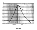
- FIG. 10 a graph of a transfer function of a filter to be implemented in accordance with the invention with upper and lower templates used in arriving at the filter design parameters.
- FIG. 2 shows an example of a simple bandpass filter in the form of an LC resonator composed of inductor 3 and capacitor 4 attached to a pair of termination resistors 5 and 6 .
- This filter has a single pair of complex poles, one zero at infinite frequency and one zero at zero frequency.
- the Q of the single pole-pair is the same as the Q of the resonator.
- FIG. 3 shows three different transfer functions 7 , 8 and 9 for different values of Q for this filter as the value of the termination resistors are changed. It can be seen that the main difference between these curves is in the gain in the passband region, while the transition and stopband regions remain largely unaffected. This observation can be extended to higher order filters: by accepting some departure from a desirable shape of the passband region, the specified selectivity properties can be achieved with low Q components and subsequently, if needed, adequate signal post-processing can restore the desired shape in the passband region.
- Highly selective filters are associated with transfer functions having high Q poles.
- the Q's of the transfer function of a passive filter can have larger magnitude than that of the individual Q's of the reactive components.
- the present invention is based on making the intrinsic losses of the integrated reactive components the main mechanism for energy dissipation within the network. However, if more energy dissipation is needed, termination resistors can be added.
- this invention pertains to the construction of selective filters with integrated lossy elements such as spiral inductors and capacitors, either of constant or variable value. This invention will be illustrated in the implementation of a narrowband bandpass filter.
- FIG. 4 shows a model for a lossy resonator.
- lossy it is meant that the resonator components exhibit a Q of less than about 20.
- Resistor 10 represents the losses of inductor 11
- resistor 12 represents the losses of capacitor 13 . Equations (2) and (3) above can be used to quantify the Q of these components by making L the inductance of 11 , C the capacitance of 13 , r the resistance of 10 and g the conductance of 12 .
- the resistors representing the losses of the resonators are not shown in the drawings described.
- FIG. 5 shows the schematics of an eighth-order bandpass filter with a structure as described in Dishal's paper.
- This topology is based on a multiplicity of coupled resonators 14 , 15 , 16 and 17 .
- Resonators 14 and 15 are inductively coupled by mutual inductance 18 .
- Resonators 16 and 17 are also inductively coupled by mutual inductance 19 .
- Resonators 15 and 16 are capacitively coupled by capacitor 20 .
- a suitable filter design program such as FLOP can yield a desired response by giving proper values for each component, that is, for the inductances and capacitances of each resonator, as well as for the mutual capacitive and inductive coefficients.
- FIGS. 6A and 6B graphically illustrate a known resonator configuration implemented in standard CMOS technology.
- standard CMOS technology several layers of metallization are typically deposited over the active layers of the CMOS chip provided on the chip's silicon substrate. These metallization layers are separated by insulation layers, typically silicon dioxide, and serve as interconnecting components of the chip. The number of metallization layers vary, but typically five or more layers are used.
- the metallization layers and insulation layers have thichness on the order of one micron, with the upper metallization layers tending to be somewhat thicker than the lower metallization layers.
- the resonator 21 is seen to be formed in several of the metallization layers of the CMOS chip (the insulation layers and active layers, other than a graphical representation of the silicon substrate, are not shown).
- the resonator components include a planar spiral inductor 23 formed in an upper metallization layer and a planar tuning capacitor formed in two of the metallization layers below the spiral inductor. (These elements are formed in the metallization layers using fabrication techniques, such as photo lithography, well known in the art.)
- the shown planar capacitor is comprised of bottom capacitor plate 25 and a top capacitor plate 29 in opposed relation over the top capacitor plate.
- the ends of the spiral inductor are connected to the tap connectors of the capacitor plates by conductive interconnection plugs (“vias”), such as the vias 35 and 37 shown in FIG. 6B .
- CMOS chip represents only three metallization layers of the CMOS chip and that CMOS chip would typically include further metallization layers, including, for example, metallization layers beneath bottom capacitor plate 25 or above spiral inductor 23 .
- the spiral inductor preferably resides in the chip's topmost metallization layer. This allows for a spiral conductor having a larger thickness (e.g. >1 ⁇ ) and maximum spacing between the spiral inductor and the chip's silicon substrate 33 .
- the material chosen for the metallization layers of the CMOS chip, and hence the material of which the spiral inductor and 23 and capacitor plates 25 are formed, is typically aluminum, copper, gold or some low-resistivity alloy.
- the attainable Q for such micro-thin resonator components ranges between 5 and 20.
- the parasitic capacitance (not shown) between the spiral and the substrate 33 (ground plane) will affect the Q of these components and should be taken into account when computing the resonant frequency of the resonator.
- FIGS. 7A and 7B show the general implementation of more than one spiral inductor using CMOS technology and the coupling of such inductors in a manner that achieves a selective filter in accordance with the invention.
- Tap connectors or terminals are provided at the end-points of the spirals of each of the spiral inductors 39 , 43 .
- the lower spiral inductor 43 is seen to have an outer tap connector 47 at the outer terminus of the spiral and a center tap connector at the center terminus of the spiral.
- the upper spiral inductor is seen to have an outer tap connector 55 and a center tap connector 59 . It is noted that the inductance of the spiral inductors depends on several variables such as:
- the value of the Q of the spiral inductors shown in FIGS. 7A and 7B is affected not only by the resistivity of the micro-thin metal layer used for building the spirals, but also by capacitive coupling between the spirals and the chip's silicon substrate 57 (the ground plane).
- the shorter the distance between the spiral and the ground plane the greater the parasitic capacitance and hence lower the Q.
- Parasitic capacitance reduces the Q because it reduces the effective value of the spiral inductance while the series resistance of the lossy inductor remains essentially unaffected.
- spiral inductors 39 , 43 The relative placement of spiral inductors 39 , 43 is used as the principal means of controlling this coupling. As spiral inductor 39 is slid in the direction of arrow 64 , the coupling coefficient increases and reaches a maximum when the two spiral centers are aligned, that is, completely overlap. The coupling coefficient K directly affects the value of mutual inductance M between the two inductors.
- the significant parameters characterizing a group of one or more interacting planar spiral inductors can be calculated from geometrical and material characteristics by using electromagnetic analysis tools.
- Software packages such as ASITIC can be used for aiding in these calculations.
- FIG. 8 shows an implementation of a pair of coupled resonators 66 , 68 in accordance with the invention using CMOS technology.
- Each of the resonators includes a planar spiral inductor 65 , 71 connected to top and bottom capacitor plates 67 , 69 and 73 , 75 in the manner of the single resonator shown in FIGS. 6A and 6B .
- the resonators are coupled together by means of their spiral inductors 65 and 71 which are overlapped as shown and described in FIGS. 7A and 7B .
- the degree to which the spiral inductors are overlapped will determine the mutual inductance between the spiral inductors and its effect on the filter's transfer function. A process for arriving at the overlap needed for a desired filter performance is described below.
- FIG. 9 is a representation of three cascaded LC resonators 76 , 78 , 80 as might be implemented using CMOS technology in a manner previously described to produce a higher order bandpass filter in accordance with the invention.
- the resonator 76 is comprised of spiral inductor 77 connected to top and bottom capacitor plates 79 , 81 ;
- resonator 78 is comprised of spiral inductor 83 connected to top and bottom capacitor plates 85 , 87 ;
- resonator 80 is comprised of spiral inductor 89 connected to top and bottom capacitor plates 91 , 93 .
- Spiral inductor 77 of resonator 76 overlaps and is coupled to spiral inductor 83 of resonator 78 .
- Spiral inductor 83 of resonator 78 overlaps and is coupled to spiral inductor 89 of resonator 80 .
- Additional similarly contructed resonators could be added to this casade of coupled reson
- a pair of templates a lower template 95 and an upper template 97 , are established to set the limits for the desired final frequency response. Every point of the frequency response should remain within the boundaries of the lower and upper templates.
- the order of the filter is initially guessed. So, for example, if the order is eight, then four resonators are required. A precise model for each resonator then has to be formalized. It should include besides the inductances and capacitances, all the resistances representing the loss mechanisms. This will result in a complex network of capacitors, inductors and resistors.
- An adequate program such as FLOP can be subsequently used to find the values of each component in such a way that the response fits within the established upper and lower templates. If the response does not fit within the template mask, an increase in the order of the filter may be necessary. Also, if the response fits too loosely, meaning that all the response points are far from the templates, then a reduction in the order of the filter may be possible. Finally, a program such as ASITIC can be used to solve the physical dimensions of the components based on the values found by FLOP. In particular, for the filter example above, it is found that the inductive coupling coefficient ranges around a value of K ⁇ 0.1, that is easily achieved. Naturally, other prescribed conditions would yield different values of K.
Landscapes
- Filters And Equalizers (AREA)
Abstract
Description
where N≦M for any passive network. The complex constants zi are called the zeros and the pj are the poles. As can be seen from (1), both the values of the poles and zeros determine the shape of the transfer function. If the network is passive and loss-less, the zeros are imaginary numbers (the real part equals zero). The poles are complex numbers where the real part is negative. The ratio between the imaginary and real parts of the poles is called the Q (to be distinguished from the Q of the electrical components implementing the filter).
where L is the inductance and r is the series resistance. For the case of a capacitor, the Q is:
where C is the capacitance and g is the parallel conductance. In a loss-less component, the Q0 in (2) and (3) is infinity.
-
- (1) the cancellation circuit can use a significant amount of silicon area (die area) and consume considerable power;
- (2) the unavoidable non-linearity of the cancellation circuitry creates a response that is a function of the signal amplitude, thus making many of the most critical specifications of related applications very hard to meet;
- (3) the transistors in the cancellation circuitry introduce noise on the signal path;
- (4) an additional complex control architecture is needed for adjusting the amount of cancellation, and inaccuracies of this cancellation could yield unstable operating conditions;
- (5) this control circuitry further consumes large amounts of power and die area; and
- (6) as shown in (4), because of the dependency on ω, the cancellation achieved does not extend evenly through the whole passband region, thus creating inaccuracies in the resulting response.
M 21
where:
M21
K21
L21, L22 are the inductances of
Claims (15)
Priority Applications (1)
| Application Number | Priority Date | Filing Date | Title |
|---|---|---|---|
| US12/082,922 US8058950B1 (en) | 2003-07-22 | 2008-04-14 | Highly selective passive filters using low-Q planar capacitors and inductors |
Applications Claiming Priority (3)
| Application Number | Priority Date | Filing Date | Title |
|---|---|---|---|
| US48958203P | 2003-07-22 | 2003-07-22 | |
| US89866604A | 2004-07-22 | 2004-07-22 | |
| US12/082,922 US8058950B1 (en) | 2003-07-22 | 2008-04-14 | Highly selective passive filters using low-Q planar capacitors and inductors |
Related Parent Applications (1)
| Application Number | Title | Priority Date | Filing Date |
|---|---|---|---|
| US89866604A Continuation-In-Part | 2003-07-22 | 2004-07-22 |
Publications (1)
| Publication Number | Publication Date |
|---|---|
| US8058950B1 true US8058950B1 (en) | 2011-11-15 |
Family
ID=44906930
Family Applications (1)
| Application Number | Title | Priority Date | Filing Date |
|---|---|---|---|
| US12/082,922 Expired - Fee Related US8058950B1 (en) | 2003-07-22 | 2008-04-14 | Highly selective passive filters using low-Q planar capacitors and inductors |
Country Status (1)
| Country | Link |
|---|---|
| US (1) | US8058950B1 (en) |
Cited By (8)
| Publication number | Priority date | Publication date | Assignee | Title |
|---|---|---|---|---|
| US20110304014A1 (en) * | 2010-06-10 | 2011-12-15 | Stmicroelectronics (Tours) Sas | Passive integrated circuit |
| US20130069753A1 (en) * | 2011-09-16 | 2013-03-21 | Witricity Corporation | High frequency pcb coils |
| US20130154765A1 (en) * | 2011-12-14 | 2013-06-20 | Siliconware Precision Industries Co., Ltd. | Cross-coupled bandpass filter |
| US20140140028A1 (en) * | 2012-11-21 | 2014-05-22 | Cambridge Silicon Radio Limited | Magnetic Coupling and Cancellation Arrangement |
| EP3154194A1 (en) * | 2015-10-05 | 2017-04-12 | Huawei Technologies Co., Ltd. | Electric filter comprising a transformer |
| US9917479B2 (en) | 2014-04-16 | 2018-03-13 | Witricity Corporation | Wireless energy transfer for mobile device applications |
| US10658016B1 (en) * | 2018-12-10 | 2020-05-19 | Integrated Device Technology, Inc. | Series continuous time linear equalizers |
| CN117688901A (en) * | 2023-12-11 | 2024-03-12 | 曲阜师范大学 | Circuit design method, system, device and storage medium for high-frequency discrete filter |
Citations (6)
| Publication number | Priority date | Publication date | Assignee | Title |
|---|---|---|---|---|
| US5656849A (en) * | 1995-09-22 | 1997-08-12 | International Business Machines Corporation | Two-level spiral inductor structure having a high inductance to area ratio |
| US6370033B1 (en) * | 1999-02-02 | 2002-04-09 | Toko Kabushiki Kaisha | Electronic device having printed circuit board joined to cavity resonance filter |
| US6549097B2 (en) * | 2000-10-24 | 2003-04-15 | Memscap | Electrical resonator with a ribbon loop and variable capacitors formed at the parallel ends |
| US6856499B2 (en) * | 2003-03-28 | 2005-02-15 | Northrop Gurmman Corporation | MEMS variable inductor and capacitor |
| US6970057B2 (en) * | 2004-04-02 | 2005-11-29 | Chi Mei Communication Systems, Inc. | Lowpass filter formed in a multi-layer ceramic |
| US7002434B2 (en) * | 2004-03-16 | 2006-02-21 | Chi Mei Communication Systems, Inc. | Lumped-element transmission line in multi-layered substrate |
-
2008
- 2008-04-14 US US12/082,922 patent/US8058950B1/en not_active Expired - Fee Related
Patent Citations (6)
| Publication number | Priority date | Publication date | Assignee | Title |
|---|---|---|---|---|
| US5656849A (en) * | 1995-09-22 | 1997-08-12 | International Business Machines Corporation | Two-level spiral inductor structure having a high inductance to area ratio |
| US6370033B1 (en) * | 1999-02-02 | 2002-04-09 | Toko Kabushiki Kaisha | Electronic device having printed circuit board joined to cavity resonance filter |
| US6549097B2 (en) * | 2000-10-24 | 2003-04-15 | Memscap | Electrical resonator with a ribbon loop and variable capacitors formed at the parallel ends |
| US6856499B2 (en) * | 2003-03-28 | 2005-02-15 | Northrop Gurmman Corporation | MEMS variable inductor and capacitor |
| US7002434B2 (en) * | 2004-03-16 | 2006-02-21 | Chi Mei Communication Systems, Inc. | Lumped-element transmission line in multi-layered substrate |
| US6970057B2 (en) * | 2004-04-02 | 2005-11-29 | Chi Mei Communication Systems, Inc. | Lowpass filter formed in a multi-layer ceramic |
Non-Patent Citations (1)
| Title |
|---|
| Nguyen et al , "Si IC Compatible Inductors and LC Passive Filter", Aug. 1990, IEEE Journal of Solid State Circuits, vol. 25, No. 4, pp. 1028-1031. * |
Cited By (12)
| Publication number | Priority date | Publication date | Assignee | Title |
|---|---|---|---|---|
| US20110304014A1 (en) * | 2010-06-10 | 2011-12-15 | Stmicroelectronics (Tours) Sas | Passive integrated circuit |
| US9117693B2 (en) * | 2010-06-10 | 2015-08-25 | Stmicroelectronics (Tours) Sas | Passive integrated circuit |
| US20130069753A1 (en) * | 2011-09-16 | 2013-03-21 | Witricity Corporation | High frequency pcb coils |
| US20130154765A1 (en) * | 2011-12-14 | 2013-06-20 | Siliconware Precision Industries Co., Ltd. | Cross-coupled bandpass filter |
| US9196941B2 (en) * | 2011-12-14 | 2015-11-24 | Siliconware Precision Industries Co., Ltd. | Cross-coupled bandpass filter |
| US20140140028A1 (en) * | 2012-11-21 | 2014-05-22 | Cambridge Silicon Radio Limited | Magnetic Coupling and Cancellation Arrangement |
| US9917479B2 (en) | 2014-04-16 | 2018-03-13 | Witricity Corporation | Wireless energy transfer for mobile device applications |
| EP3154194A1 (en) * | 2015-10-05 | 2017-04-12 | Huawei Technologies Co., Ltd. | Electric filter comprising a transformer |
| US10658016B1 (en) * | 2018-12-10 | 2020-05-19 | Integrated Device Technology, Inc. | Series continuous time linear equalizers |
| US20200185013A1 (en) * | 2018-12-10 | 2020-06-11 | Integrated Device Technology, Inc. | Series continuous time linear equalizers |
| CN117688901A (en) * | 2023-12-11 | 2024-03-12 | 曲阜师范大学 | Circuit design method, system, device and storage medium for high-frequency discrete filter |
| CN117688901B (en) * | 2023-12-11 | 2024-05-14 | 曲阜师范大学 | Circuit design method, system, device and storage medium for high frequency discrete filter |
Similar Documents
| Publication | Publication Date | Title |
|---|---|---|
| US8058950B1 (en) | Highly selective passive filters using low-Q planar capacitors and inductors | |
| US5497337A (en) | Method for designing high-Q inductors in silicon technology without expensive metalization | |
| US6160303A (en) | Monolithic inductor with guard rings | |
| US6429504B1 (en) | Multilayer spiral inductor and integrated circuits incorporating the same | |
| US10447228B2 (en) | High quality factor time delay filters using multi-layer fringe capacitors | |
| US6201287B1 (en) | Monolithic inductance-enhancing integrated circuits, complementary metal oxide semiconductor (CMOS) inductance-enhancing integrated circuits, inductor assemblies, and inductance-multiplying methods | |
| EP0862218B1 (en) | An improved-q inductor with multiple metalization levels | |
| US7091814B2 (en) | On-chip differential multi-layer inductor | |
| US7869784B2 (en) | Radio frequency circuit with integrated on-chip radio frequency inductive signal coupler | |
| US20060141979A1 (en) | Radio frequency circuit with integrated on-chip radio frequency signal coupler | |
| US5485131A (en) | Transmission line filter for MIC and MMIC applications | |
| US8390386B2 (en) | Variable inductor | |
| US20070085649A1 (en) | Spiral inductor having variable inductance | |
| US6608361B2 (en) | On-chip inductor using active magnetic energy recovery | |
| US7236080B2 (en) | On-chip high Q inductor | |
| JP4471757B2 (en) | Variable inductor | |
| JP4211994B2 (en) | High frequency filter | |
| US6549097B2 (en) | Electrical resonator with a ribbon loop and variable capacitors formed at the parallel ends | |
| JPH08222695A (en) | Inductor element and manufacturing method thereof | |
| US20100133652A1 (en) | Semiconductor device and method of manufacturing the same | |
| US7423490B2 (en) | Wideband high frequency chokes | |
| Lee et al. | Design and analysis of symmetric dual-layer spiral inductors for RF integrated circuits | |
| JPH0774311A (en) | Semiconductor analog integrated circuit | |
| Malba et al. | High-performance RF coil inductors on silicon | |
| KR100393774B1 (en) | Manufacturing method for bandpass filter using thin film bulk acoustic resonator |
Legal Events
| Date | Code | Title | Description |
|---|---|---|---|
| ZAAA | Notice of allowance and fees due |
Free format text: ORIGINAL CODE: NOA |
|
| ZAAB | Notice of allowance mailed |
Free format text: ORIGINAL CODE: MN/=. |
|
| STCF | Information on status: patent grant |
Free format text: PATENTED CASE |
|
| REMI | Maintenance fee reminder mailed | ||
| FPAY | Fee payment |
Year of fee payment: 4 |
|
| SULP | Surcharge for late payment | ||
| MAFP | Maintenance fee payment |
Free format text: PAYMENT OF MAINTENANCE FEE, 8TH YR, SMALL ENTITY (ORIGINAL EVENT CODE: M2552); ENTITY STATUS OF PATENT OWNER: SMALL ENTITY Year of fee payment: 8 |
|
| FEPP | Fee payment procedure |
Free format text: MAINTENANCE FEE REMINDER MAILED (ORIGINAL EVENT CODE: REM.); ENTITY STATUS OF PATENT OWNER: SMALL ENTITY |
|
| LAPS | Lapse for failure to pay maintenance fees |
Free format text: PATENT EXPIRED FOR FAILURE TO PAY MAINTENANCE FEES (ORIGINAL EVENT CODE: EXP.); ENTITY STATUS OF PATENT OWNER: SMALL ENTITY |
|
| STCH | Information on status: patent discontinuation |
Free format text: PATENT EXPIRED DUE TO NONPAYMENT OF MAINTENANCE FEES UNDER 37 CFR 1.362 |
|
| FP | Lapsed due to failure to pay maintenance fee |
Effective date: 20231115 |