US8055217B2 - Adaptive complex gain predistorter for a transmitter - Google Patents
Adaptive complex gain predistorter for a transmitter Download PDFInfo
- Publication number
- US8055217B2 US8055217B2 US12/413,109 US41310909A US8055217B2 US 8055217 B2 US8055217 B2 US 8055217B2 US 41310909 A US41310909 A US 41310909A US 8055217 B2 US8055217 B2 US 8055217B2
- Authority
- US
- United States
- Prior art keywords
- signal
- lookup table
- complex
- tilde over
- lut
- Prior art date
- Legal status (The legal status is an assumption and is not a legal conclusion. Google has not performed a legal analysis and makes no representation as to the accuracy of the status listed.)
- Active, expires
Links
- 230000003044 adaptive effect Effects 0.000 title claims description 40
- 238000010606 normalization Methods 0.000 claims abstract description 61
- 238000000034 method Methods 0.000 claims description 42
- 230000001413 cellular effect Effects 0.000 claims description 15
- 230000007246 mechanism Effects 0.000 claims description 15
- 238000012545 processing Methods 0.000 claims description 14
- 230000008569 process Effects 0.000 claims description 9
- 230000004044 response Effects 0.000 claims description 6
- 230000003111 delayed effect Effects 0.000 claims description 3
- 238000001514 detection method Methods 0.000 claims description 3
- 238000004891 communication Methods 0.000 description 13
- 238000010586 diagram Methods 0.000 description 12
- 230000006978 adaptation Effects 0.000 description 10
- 238000012360 testing method Methods 0.000 description 8
- 230000006870 function Effects 0.000 description 7
- 238000013461 design Methods 0.000 description 6
- 230000005540 biological transmission Effects 0.000 description 5
- 238000012937 correction Methods 0.000 description 4
- 230000003287 optical effect Effects 0.000 description 4
- 238000004422 calculation algorithm Methods 0.000 description 3
- 238000004364 calculation method Methods 0.000 description 3
- 239000013078 crystal Substances 0.000 description 3
- 230000003993 interaction Effects 0.000 description 3
- 230000010363 phase shift Effects 0.000 description 3
- 230000002829 reductive effect Effects 0.000 description 3
- 230000003068 static effect Effects 0.000 description 3
- 238000007792 addition Methods 0.000 description 2
- 238000013459 approach Methods 0.000 description 2
- 230000008901 benefit Effects 0.000 description 2
- 230000015556 catabolic process Effects 0.000 description 2
- 238000006243 chemical reaction Methods 0.000 description 2
- 238000006731 degradation reaction Methods 0.000 description 2
- 238000005516 engineering process Methods 0.000 description 2
- 238000013507 mapping Methods 0.000 description 2
- 239000004065 semiconductor Substances 0.000 description 2
- 238000010897 surface acoustic wave method Methods 0.000 description 2
- 102100024394 Adipocyte enhancer-binding protein 1 Human genes 0.000 description 1
- 238000012935 Averaging Methods 0.000 description 1
- 101000833122 Homo sapiens Adipocyte enhancer-binding protein 1 Proteins 0.000 description 1
- 230000003213 activating effect Effects 0.000 description 1
- 230000032683 aging Effects 0.000 description 1
- 230000003321 amplification Effects 0.000 description 1
- 230000006399 behavior Effects 0.000 description 1
- 230000010267 cellular communication Effects 0.000 description 1
- 239000002131 composite material Substances 0.000 description 1
- 230000006835 compression Effects 0.000 description 1
- 238000007906 compression Methods 0.000 description 1
- 230000008878 coupling Effects 0.000 description 1
- 238000010168 coupling process Methods 0.000 description 1
- 238000005859 coupling reaction Methods 0.000 description 1
- 230000001934 delay Effects 0.000 description 1
- 230000001419 dependent effect Effects 0.000 description 1
- 230000000694 effects Effects 0.000 description 1
- 230000002401 inhibitory effect Effects 0.000 description 1
- 230000010354 integration Effects 0.000 description 1
- 230000000670 limiting effect Effects 0.000 description 1
- 238000001459 lithography Methods 0.000 description 1
- 238000004519 manufacturing process Methods 0.000 description 1
- 238000005259 measurement Methods 0.000 description 1
- 230000005055 memory storage Effects 0.000 description 1
- 239000000203 mixture Substances 0.000 description 1
- 238000010295 mobile communication Methods 0.000 description 1
- 238000012986 modification Methods 0.000 description 1
- 230000004048 modification Effects 0.000 description 1
- 238000003199 nucleic acid amplification method Methods 0.000 description 1
- 238000005457 optimization Methods 0.000 description 1
- 238000012163 sequencing technique Methods 0.000 description 1
- 238000004088 simulation Methods 0.000 description 1
- 239000007787 solid Substances 0.000 description 1
- 230000003595 spectral effect Effects 0.000 description 1
- 239000000758 substrate Substances 0.000 description 1
- 230000001360 synchronised effect Effects 0.000 description 1
Images


Classifications
-
- H—ELECTRICITY
- H03—ELECTRONIC CIRCUITRY
- H03F—AMPLIFIERS
- H03F1/00—Details of amplifiers with only discharge tubes, only semiconductor devices or only unspecified devices as amplifying elements
- H03F1/32—Modifications of amplifiers to reduce non-linear distortion
- H03F1/3241—Modifications of amplifiers to reduce non-linear distortion using predistortion circuits
- H03F1/3247—Modifications of amplifiers to reduce non-linear distortion using predistortion circuits using feedback acting on predistortion circuits
-
- H—ELECTRICITY
- H03—ELECTRONIC CIRCUITRY
- H03F—AMPLIFIERS
- H03F3/00—Amplifiers with only discharge tubes or only semiconductor devices as amplifying elements
- H03F3/20—Power amplifiers, e.g. Class B amplifiers, Class C amplifiers
- H03F3/24—Power amplifiers, e.g. Class B amplifiers, Class C amplifiers of transmitter output stages
-
- H—ELECTRICITY
- H03—ELECTRONIC CIRCUITRY
- H03F—AMPLIFIERS
- H03F2201/00—Indexing scheme relating to details of amplifiers with only discharge tubes, only semiconductor devices or only unspecified devices as amplifying elements covered by H03F1/00
- H03F2201/32—Indexing scheme relating to modifications of amplifiers to reduce non-linear distortion
- H03F2201/3233—Adaptive predistortion using lookup table, e.g. memory, RAM, ROM, LUT, to generate the predistortion
Definitions
- the invention is directed, in general, to wireless transmitters and, more specifically, to an apparatus and method for adaptive Cartesian transmitter linearization and a wireless transmitter for use in cellular telephony and communication devices such as Bluetooth, WLAN, etc. using all-digital radio frequency (RF) circuitry.
- RF radio frequency
- NodeB Wireless cellular communication networks incorporate large numbers of mobile user equipment (UEs) and a number of base nodes (NodeBs).
- a NodeB is generally a fixed station, and may also be called a base transceiver system (BTS), an access point (AP), a base station (BS), or some other equivalent terminology.
- BTS base transceiver system
- AP access point
- BS base station
- eNB evolved NodeB
- NodeB hardware when deployed, is fixed and stationary, while the UE hardware is typically portable.
- the mobile UE can comprise portable hardware.
- User equipment also commonly referred to as a terminal or a mobile station, may be fixed or mobile device and may be a wireless device, a cellular phone, a personal digital assistant (PDA), a wireless modem card, and so on.
- UL uplink communication
- DL downlink
- Each NodeB contains radio frequency transmitter(s) and the receiver(s) used to communicate directly with the mobiles, which move freely around it.
- each mobile UE contains radio frequency transmitter(s) and the receiver(s) used to communicate directly with the NodeB. In cellular networks, the mobiles cannot communicate directly with each other but have to communicate with the NodeB.
- Digital radio has recently allowed the replacement of space consuming analog RF circuitry with much more compact digital circuitry, thereby facilitating the ability to port designs rapidly to more advanced lithographies.
- Texas Instruments (TI) has proven this concept with its Digital RF Processor (DRPTM) architecture, which it has successfully implemented in production versions of its Bluetooth BRF6xxx transceivers, GSM/GPRS LoCosto TCS23xx transceivers among other chips.
- DRP implementation is consistent with the on-going trend toward RF-CMOS in the cellular area, making it attractive in terms of power consumption, cost, and the integration of multiple radios.
- Transmitters use one or more amplifiers, such as a digital pre-power amplifier (PPA) and an external power amplifier (PA), to amplify components of the input signal to be transmitted. These components are in-phase and quadrature components in the case of a Cartesian transmitter.
- PPA digital pre-power amplifier
- PA external power amplifier
- a highly linear amplifier distorts the signal the least and so is most favored from a standpoint of signal quality.
- highly linear amplifiers use relatively large amounts of power and numbers of highly accurate and tightly matched components, making them relatively power consumptive, large and expensive. Though they perform the best, they are thus disfavored in many wireless applications, particularly those that require low-cost transmitters or transmitters that are subject to large operating voltage excursions.
- the amplifier that is best suited overall for low-cost, battery-powered wireless transmitters is a simpler amplifier having significant nonlinearities.
- Predistortion is often used to compensate for these nonlinearities, resulting in a linearization of the output of the amplifier.
- the theory underlying predistortion is that if an amplifier's distortion characteristics are known in advance, an inverse function can be applied to an input signal to predistort it before it is provided to the amplifier. Though the amplifier then distorts the signal as it amplifies it, the predistortion and the amplifier distortion essentially cancel one another, resulting in an amplified output signal having substantially reduced distortion.
- DPD digital predistortion
- LUT lookup table
- Entries in the LUT are addressed using samples of the input signal.
- the output values retrieved from the LUT are used either to modify the samples (an “inverse gain” configuration) or in lieu of the samples (a “direct mapping” configuration).
- samples are transmitted at a very high rate.
- the predistorter needs to be able to look up and retrieve output values very quickly.
- WCDMA Cartesian transmitters suffer nonlinearities resulting from both amplitude modulation (AM) and phase modulation (PM), namely AM-AM and AM-PM interactions, occurring in their amplifier(s).
- AM amplitude modulation
- PM phase modulation
- predistortion is carried out at least partially to negate the effect of these interactions.
- a nominal predistortion LUT Values for a nominal predistortion LUT are typically computed during initial factory calibration. Unfortunately, a factory-calibrated predistortion LUT often fails to linearize the amplifier(s) adequately under varying operational conditions (e.g., temperature, voltage, frequency and voltage standing-wave ratio, or VSWR). Aging, especially in WCDMA and other so-called “3G” transmitters, only exacerbates the inadequacy.
- FIG. 1 is a pictorial of an illustrative telecommunications network that employs an embodiment of adaptive gain normalization and predistortion in transceivers used in the network;
- FIG. 2 is a block diagram of a single-chip radio with an all-digital local oscillator and transmitter that performs predistortion;
- FIGS. 3A and 3B are plots illustrating nonlinear operation of the transmitter of FIG. 2 ;
- FIGS. 4A and 4B are plots illustrating typical Class A and Class C, respectively, operation of the transmitter amplifier of FIG. 2 ;
- FIG. 5 is a more detailed block diagram of the transmitter portion of the radio of FIG. 2 that embodies adaptive gain normalization and predistortion;
- FIG. 6 is a more detailed block diagram of the adaptive predistortion mechanism of the transmitter of FIG. 5 ;
- FIGS. 7A and 7B are plots illustrating entries in a complex look up table used in the predistortion mechanism of FIG. 6 ;
- FIG. 8 is a block diagram illustrating the adaptive gain/phase normalization mechanism of FIG. 6 ;
- FIG. 9 is a flow diagram illustrating operation of the adaptive normalization and predistortion
- FIGS. 10A and 10B are plots comparing EVM and ACLR1, respectively, performance with adaptive gain/phase normalization
- FIG. 11 is a block diagram illustrating a module to determine approximate amplitude for indexing the look up tables of FIG. 6 ;
- FIG. 12 is a block diagram of a cellular telephone with an embodiment of a transmitter using adaptive normalization and predistortion.
- Embodiments of the present invention include adaptive digital linearization techniques for a Cartesian WCDMA transmitter.
- a digital Predistortion block implemented as a digital lookup table (LUT) is used to predistort the complex baseband signal (Inphase and Quadrature components) of a WCDMA Cartesian transmitter.
- the transmitter non-linearity is assumed to be dominant in the post combination devices such as Pre-power Amplifier (PPA) and/or the external Power amplifier. As result the dominant nonlinearity will be a function of the complex magnitude of the baseband signal as opposed to the magnitude of Inphase and Quadrature components (such as is the case for the DAC and mixer nonlinearity).
- DSP digital RF processor
- GSM Global System for Mobile communication
- Bluetooth Wireless Fidelity
- WCDMA Wideband Code Division Multiple Access
- the invention is not limited to use with any particular communication standard and may be used in control, optical, wired and wireless applications. Further, the invention is not limited to use with a specific modulation scheme but is applicable to any modulation scheme including both digital and analog modulation.
- the term communications device is defined as any apparatus or mechanism adapted to transmit, or transmit and receive data through a medium.
- the communications device may be adapted to communicate over any suitable medium such as RF, wireless, infrared, optical, wired, microwave, etc.
- the communications device may comprise an RF transmitter, RF receiver, RF transceiver or any combination thereof.
- the notation DRP is intended to denote either a Digital RF Processor or Digital Radio Processor. References to a Digital RF Processor infer a reference to a Digital Radio Processor and vice versa.
- a least means squared (LMS) based adaptation technique may be used for a complex gain lookup table (LUT) to track the temperature variations of the transmitter's nonlinear characteristics during operation.
- the algorithm is optimized to enable a low complexity hardware implementation and provides relatively fast convergence.
- An amplitude approximation method that is suitable to address the complex gain LUT is described that avoids the computation of square root.
- an adaptive loop gain/phase normalization technique is described that avoids the appearance of curve discontinuities and maintains the accuracy of open loop power control. It reuses the existing LUT adaptation hardware and therefore is inexpensive to implement.
- FIG. 1 shows an exemplary wireless telecommunications network 100 .
- the illustrative telecommunications network includes representative base stations 101 , 102 , and 103 ; however, a telecommunications network necessarily includes many more base stations.
- Each of base stations 101 , 102 , and 103 are operable over corresponding coverage areas 104 , 105 , and 106 .
- Each base station's coverage area is further divided into cells. In the illustrated network, each base station's coverage area is divided into three cells.
- Handset or other UE 109 is shown in Cell A 108 , which is within coverage area 104 of base station 101 .
- Base station 101 is transmitting to and receiving transmissions from UE 109 via downlink 110 and uplink 111 .
- UE 109 may be handed over to base station 102 .
- a UE in a cell may be stationary such as within a home or office, or may be moving while a user is walking or riding in a vehicle.
- UE 109 moves within cell 108 with a velocity 112 relative to base station 102 .
- UE 109 is transmitting to and receiving from base station 101 voice and/or data transmissions.
- base station 101 voice and/or data transmissions.
- the UE moves around in the network and is placed in different environments such as in a pocket or purse, carried to hot or cold environments such as indoors and outdoors, placed in the sun, and so on, the resulting extreme changes in temperature will cause differences in the performance of analog components used in the transmitter.
- An adaptive loop gain/phase normalization mechanism along with an adaptive predistorter is used to compensate for these temperature variations, as will be explained in more detail below.
- FIG. 2 A block diagram illustrating a single chip radio incorporating an interpolative all-digital local oscillator based Cartesian transmitter and digitally-intensive receiver is shown in FIG. 2 .
- the transmitter as shown, is adapted for the EDGE/WCDMA cellular standards. It is appreciated, however, that one skilled in the communication arts can adapt the transmitter illustrated herein to other modulations and communication standards as well without departing from the spirit and scope of the present invention.
- This embodiment of a DRPu for UMTS is a Digital RF Processor (DRP)-based dominantly digital transceiver integrated with a digital baseband processor in 45 nm CMOS technology.
- DRP Digital RF Processor
- This DRPu EDGE/WCDMA (2.5G/3G) transmitter (TX) is based on a Cartesian (I/Q) direct up-conversion TX architecture with digital assistance for calibrations and compensation, henceforth termed as a Digitally Assisted analog I/Q (DAIQ) TX.
- DAIQ Digitally Assisted analog I/Q
- GSM 2G
- the transmitter architecture is small-signal analog polar.
- DRP supports interface with both multi-mode and multi-band power amplifiers (PA).
- the radio circuit comprises a transceiver integrated circuit (IC) 136 coupled to a crystal 152 , antenna front end module 176 connected to antenna 180 and battery management circuit 132 .
- the radio chip 136 comprises a script processor 146 , memory 142 (e.g., static RAM), transmit (TX) block 148 , receiver (RX) block 150 , digitally controlled crystal oscillator (DCXO) 154 , slicer 156 , power management unit 138 , RF built-in self test (BIST) 140 .
- Battery 134 and battery management circuit 132 are connected to radio chip 136 for providing power.
- Digital baseband (DBB) processor 144 and flash memory/EEPROM 145 is coupled to transceiver IC 136 via transceiver interface 137 .
- DBB Digital baseband
- the TX block 148 comprises high speed and low speed digital logic block 158 , digital to analog converter 160 , low pass filter 162 , amplitude modulator 168 , digitally controlled oscillator (DCO) 164 , digitally controlled pre-power amplifier 174 .
- the transmitter generates various radio frequency signals, as defined by the 3GPP specifications. For example, the transmitter may support one or more of the 3 G UMTS frequencies: 850, 900, 1700, 1900, or 2100 MHz.
- a key component of transmitter block 148 is digitally controlled oscillator (DCO) 164 , that is part of an interpolated-digital phase-locked loop (ADPLL).
- DCO 164 avoids any analog tuning controls.
- the DCO generates a high-quality base station-synchronized frequency reference such that the transmitted carrier frequencies and the received symbol rates are accurate to within 0.1 ppm. Fine frequency resolution is achieved through high-speed sigma-delta ( ⁇ ) dithering of its varactors.
- Digital logic built around the DCO realizes an interpolated all-digital PLL (ADPLL) that is used as a local oscillator for both the transmitter and receiver.
- the Cartesian transmitter architecture utilizes a digitally controlled power amplifier (DPA) 174 for the amplitude modulation. It is followed by a matching network and an external antenna front-end module 176 , which comprises a power amplifier (PA), a transmit/receive switch for the common antenna 180 and RX surface acoustic wave (SAW)
- ADPLL frequency synthesizer is described in US Patent application 2008-0315960 to Waheed et al entitled “Digital Phase Locked Loop with Gear Shifting” which is incorporated by reference herein in its entirety.
- Fixed baseband clock circuit 155 provides a fixed clock to DBB processor 144 and to transceiver interface 137 .
- Clock module 166 receives a variable clock from DCO 164 and produces a set of synchronized RF derived clocks for use by digital processing module 158 and DAC 160 .
- Clock module 166 also receives a clock signal from transceiver interface 137 that is used to allow synchronization of clocks between fixed clock 155 and variable clocks derived from DCO 164 .
- the receiver employs a discrete-time architecture in which the RF signal is directly sampled and processed using analog and digital signal processing techniques.
- RX block 150 comprises a low noise transconductance amplifier 182 , current sampler 184 , discrete time processing block 186 , analog to digital converter (ADC) 188 and digital logic block 190 .
- the receiver 150 employs a discrete-time architecture in which the RF signal is directly sampled at the Nyquist rate of the RF carrier and processed using analog and digital signal processing techniques.
- the transceiver is integrated with a script processor 146 , dedicated digital base band processor 144 (i.e. ARM family processor and DSP) and SRAM memory 142 .
- the script processor handles various TX and RX calibration, compensation, sequencing and lower-rate data path tasks and encapsulates the transceiver complexity in order to present a much simpler software programming model.
- the frequency reference (FREF) is generated on-chip by a 38.4 MHz (but could be 26.0 MHz or another frequency in another embodiment) digitally controlled crystal oscillator (DCXO).
- An integrated power management (PM) system is connected to an external battery management circuit 132 that conditions and stabilizes the supply voltage.
- the PM comprises a switched mode power supply (SMPS) as well as multiple low drop out (LDO) regulators that provide internal supply voltages and also isolate supply noise between circuits, especially protecting the DCO.
- SMPS switched mode power supply
- LDO low drop out
- the SMPS is used for efficient conversion of the battery voltage to a level that can be used by on-chip LDOs.
- the RF built-in self-test (RFBIST) 140 performs autonomous phase noise and modulation distortion testing, various loopback configurations for bit-error rate measurements and implements various DPA calibration and BIST procedures.
- the transceiver may be integrated with the digital baseband processor 144 and flash memory 145 memory in a complete system-on-chip (SoC) solution.
- SoC system-on-chip
- FIGS. 3A and 3B are plots illustrating nonlinear operation of the transmitter of FIG. 2 .
- FIG. 3A illustrates in general how nonlinear amplifier 174 , which is representative of PPA 174 in FIG. 2 , distorts a substantially sinusoidal input signal.
- predistortion module 302 is used to compensate for these nonlinearities, resulting in a linearization of the output of the amplifier.
- the theory underlying predistortion is that if an amplifier's distortion characteristics are known in advance, an inverse function can be applied to an input signal to predistort it before it is provided to the amplifier.
- the amplifier then distorts the signal as it amplifies it, the predistortion and the amplifier distortion essentially cancel one another, resulting in an amplified output signal having substantially reduced distortion in which a digital predistorter 302 predistorts the substantially sinusoidal input signal such that the output signal is likewise sinusoidal.
- Predistorter 302 is embodied as a look-up table (LUT) that is indexed by the input signal. At each instant of the input signal, the LUT is indexed by a representation of the input signal and the output of the LUT scales the input signal in response to the value at the indexed location in the LUT.
- LUT look-up table
- Predistorter 302 needs to be continually updated.
- Existing complex gain LUT predistorters with sample-based update do not address the potential discontinuities due to the local nature of the LUT update. These discontinuities appear when the temperature changes greatly and only part of the LUT is updated. This highly undesirable behavior in overcome by adaptive gain/phase normalization as will be described in more detail below.
- FIGS. 4A and 4B are plots illustrating typical Class A and Class C, respectively, operation of the transmitter amplifier of FIG. 2 .
- the nonlinearity of the PPA/PA distorts the combined RF signal.
- the distortion is caused by the amplitude depend gain and phase shift of the PPA/PA.
- the distortion is modeled by a complex gain F(r).
- the AM-AM and AM-PM are respectively given by the amplitude dependant magnitude and angle of F(r). Examples of AM-AM and AM-PM curves are shown FIGS. 4A and 4B .
- FIG. 5 is a more detailed block diagram of the transmitter portion of the radio of FIG. 2 that embodies adaptive gain normalization and predistortion in a Cartesian transmitter.
- Digital baseband processor 144 (illustrated in FIG. 2 ) produces in-phase and quadrature components I and Q.
- a filter block 505 conditions I and Q for amplification.
- Cartesian predistortion LUT 510 is a single LUT that is initially loaded with calibration based entries and then is updated adaptively. It is employed to produce predistorted amplitude and phase components I Z and Q Z .
- I Z and Q Z are converted to analog form, filtered and modulated as shown and provided to the PPA 535 , yielding the WCDMA output signal.
- I Z and Q Z are also provided to the decimator and aligner 545 to be used in temperature adaptation.
- Phase locked loop 520 is representative of the ADPLL in FIG. 2 that includes digitally controlled oscillator 164 .
- a coupler 540 provides a portion of the WCDMA output signal to the input of a receiver.
- coupler 540 is a signal trace on the circuit substrate.
- the receiver employs a low noise amplifier (LNA) 550 to yield RF signals that are then down-converted to produce in-phase and quadrature components I Y and Q Y of the WCDMA output signal, which are then filtered in low pass filters (LPF) as shown.
- LPF low pass filters
- a second Cartesian predistortion LUT 560 also has one LUT that holds complex valued entries in this embodiment. LUT 560 post-distorts I Z and Q Z .
- the differences between these amplitude and phase components and those provided via the decimator and aligner 645 are provided to a predistortion adapter 665 which updates predistortion in the complex compensation LUT of the second Cartesian predistortion LUT 560 .
- the second Cartesian predistortion LUT 560 are then exchanged with the first Cartesian predistortion LUTs 510 for the next lookup.
- the first Cartesian predistortion LUTs 510 are updated during that next lookup, the first and second Cartesian predistortion LUTs 510 , 560 are exchanged again for the lookup after that, and so on.
- the feedforward predistortion may be either a direct mapping in which the value of an incoming complex signal determines the complex predistorted value, or a complex scaling term in which the value of an incoming complex signal is scaled by the complex value in the LUT.
- the Cartesian transmitter of FIG. 5 features three potentially nonlinear elements in both of its I and Q paths. These elements include the digital-to-analog converter (DAC) 512 , the PPA 514 , possibly including AM-AM and AM-PM nonlinearities, and PA 535 , again possibly including AM-AM and AM-PM nonlinearities.
- DAC digital-to-analog converter
- FIG. 6 is a more detailed block diagram of the adaptive predistortion mechanism of the transmitter of FIG. 5 .
- the distortion is modeled by a complex gain F(r).
- the AM-AM and AM-PM are respectively given by the amplitude dependant magnitude and angle of F(r).
- An input signal X is provided to predistortion LUT 604 that contains complex predistortion scaling parameters.
- the complex output of LUT 604 and the complex input signal X are multiplied in a scaling module 606 and provided as input to a nonlinear element 608 , which provides an output signal Y.
- a receiver feeds back the output signal Y, incurring some delay.
- An output delay circuit 610 represents that delay.
- This signal is then normalized by normalization block 612 that multiples the feedback signal by a complex gain normalization parameter that is roughly equivalent to an inverse of the gain of the front end components.
- An input delay circuit 624 delays the output of scaling module 606 by an equivalent amount.
- a second compensation LUT 618 receives the normalized feedback signal ⁇ tilde over (Y) ⁇ .
- the complex output of the second compensation LUT is multiplied with the feedback signal ⁇ tilde over (Y) ⁇ in scaling module 620 .
- a summing junction 622 provides the difference signal ⁇ k between the two delayed signals to a quality monitor 626 .
- the quality monitor uses an iterative LMS-like approach to update the second compensation LUT 618 to minimize the difference. The exact method of performing the update will be described in more detail below.
- the compensation predistorter is adapted during transmission using the symbols that are being transmitted. The compensation predistorter continuously changes until a steady state is reached when the feedback error reaches zero. After an entry in second LUT 618 is updated, multiplexing logic that controls the LUTs is toggled so that the feed-forward predistortion points to the newly updated table and the adaptation points to the other LUT, as indicated at 630 .
- Adaptive gain/phase equalization module 614 updates normalization block 612 to compensate for changes in loop gain due to temperature and voltage variations that affect the operation of analog components of the transmitter.
- the transmitter's nonlinearity varies over time because of temperature fluctuations, but also fast varying loading conditions (VSWR). Inaccuracies in the gain normalization can cause the predistorter curves to vary drastically. Since the update is local this potentially causes temporary discontinuities in the LUT curves that could degrade the transmitter's performance.
- An adaptive gain normalization that reuses the predistorter update hardware mitigates this issue.
- the adaptive normalization mechanism is operable to temporarily substitute a single register for the second compensation lookup table 618 while updating the complex gain normalization parameter. As will be described in more detail below, the adaptive normalization mechanism iteratively converges on a revised gain normalization parameter using the single register to determine a complex value equal to approximately the inverse of a combined gain of the non-linear device over a linear region and components of the feedback loop, such that a resulting loop gain is approximately one.
- First LUT 604 is indexed using a representation of the input signal X. Amplitude computation through the formula ⁇ square root over ( I 2 +Q 2 ) ⁇
- Approximation module 602 determines an approximate value corresponding to each sample of input signal X that is used to index first LUT 604 .
- approximation module 616 determines an approximate value corresponding to each sample of feedback signal ⁇ tilde over (Y) ⁇ that is used to index second LUT 618 . The operation of the approximation modules will be described in more detail below.
- the predistorter is realized with a lookup table storing the imaginary and real parts of the complex gain.
- the transmitter is perfectly linearized when the following condition is satisfied:
- the present adaptation technique using a feedback path can be used for both factory self-calibration and online update.
- a low complexity update equation is obtained by applying the least mean squares (LMS) algorithm.
- LMS least mean squares
- the goal is to minimize an objective function which is the mean squared error: E (
- L ⁇ ⁇ U ⁇ ⁇ T ⁇ [ n ] ⁇ L ⁇ ⁇ U ⁇ ⁇ T ⁇ [ n ] - ⁇ 2 ⁇ ⁇ E ⁇ ⁇ ⁇ ⁇ k ⁇ 2 ⁇ ⁇ L ⁇ ⁇ U ⁇ ⁇ T ⁇ [ n ] ⁇ ⁇ L ⁇ ⁇ U ⁇ ⁇ T ⁇ [ n ] + ⁇ ⁇ Y ⁇ * ⁇ ⁇ k ( 1 )
- LUT[n] indicates an entry in the second compensation lookup table
- ⁇ tilde over (Y) ⁇ * is a complex conjugate value of the normalized feedback signal ⁇ tilde over (Y) ⁇ .
- ⁇ k is an error signal corresponding to a difference between pre-distorted signal Z and post-distorted signal Zfb; and
- ⁇ is an update factor (real-valued) that controls the speed of convergence.
- FIGS. 7A and 7B are plots illustrating entries in a complex look up table used in the predistortion mechanism of FIG. 6 . These entries are determined by quality monitor 626 performing the update operation described above.
- the complex gain LUT[n] also referred to as G(n) is obtained by looking up an entry in the LUT indexed by a representative value of feedback signal Y.
- G(n) A nearest neighbor LUT is considered here, but the optimization presented here is also applicable to linearly interpolation and higher orders of interpolation.
- LUT[ n ] LUT[ n]+ ⁇ G
- ⁇ G ⁇ k ⁇ ( I o ⁇ jQ o ) ⁇ k
- k is the quadrant number containing a vector (I o +jQ o ) corresponding to normalized feedback signal ⁇ tilde over (Y) ⁇
- ⁇ is an update factor (real-valued) that controls the speed of convergence.
- the predistortion update mechanism is very sensitive to loop gain normalization variations. It must therefore be very accurate.
- the initial computed normalization 1/K used in normalization module 612 which is the product of the TX gain, the coupling factor and the LNA gain, for normalization is only an estimate and is not expected to be very accurate, due to intractable temperature variations etc. . . . Therefore an adaptive gain normalization block 614 is used to improve the normalization accuracy.
- An adaptive loop gain normalization block 614 is introduced for the following reasons:
- adaptive loop gain normalization block 614 is roughly represented by adaptive normalization mechanism 806 .
- Forward compensation block 802 represents LUT 604 and related circuitry.
- Adaptation module 804 represents LUT 618 and related circuitry.
- linear regions 402 , 404 are in a range of approximately 12 dB back-off or more.
- the update equation for ⁇ is similar to the predistorter update.
- the LUT is simply replaced by the register 808 containing ⁇ . This can be done with a multiplexor or other selection logic.
- the same hardware can be reused since the predistorter update should be activated only after correct loop normalization is done.
- the only additional function is the required testing to determine if the signal is in the linear region. This is implemented very efficiently if the chosen threshold is a power of 2, in which case update logic 626 only needs to test a single bit. It should be noted that the convergence of ⁇ is several orders of magnitude faster than the predistortion LUT convergence since all qualifying samples are used to update a single register as opposed to several entries of the LUT.
- a correction by a real factor ⁇ must be performed.
- This factor ⁇ must be greater than or equal to the maximum compression at peak code, over all operating conditions (process, voltage, temperature, VSWR etc. . . . ). It is used to make sure that the peak signal amplitude at the output of the predistorter is equal or less than the input's, so that the same bit representation is maintained at both input and output ports. The magnitude of the LUT gain will therefore be maintained less than 1. If this additional correction is skipped then the predistorter will expand the range of the feed forward predistortion output signal potentially causing overflows unless the bit width of the output is adequately set.
- the normalization factors ⁇ and 1/K, and the real correction factor ⁇ are combined 810 into a single complex multiplier and stored in the 1/K register 812 by the script processor prior to activating predistortion update.
- FIG. 9 A flow chart of the adaptive gain normalization is shown in FIG. 9 .
- an adaptive gain/phase normalization operation is performed. To begin, an estimated 1/K value is selected 902 and placed in 1/K register 812 .
- ⁇ register 808 is initialized to 1+j0.
- Selection multiplexers are configured 904 to select ⁇ register 808 in place of predistortion adjustment LUT 618 .
- a time counter is then initialized 906 .
- Samples of complex input signal Z are tested 908 to determine if they are in the linear region of nonlinear device 608 . If yes, then ⁇ register 808 is updated 910 ; otherwise the time count is incremented 908 and the linearity test repeated on the next sample of input signal Z. This process repeats until ⁇ and 1/K converge 912 or until the time counter expires. Typically, convergence occurs in less than 10 us. At this point, ⁇ register 808 and 1/K normalization register 812 are multiplied together and scaled 914 by a predetermined constant ⁇ value in order to guarantee the magnitude of the LUT gain will be maintained less than 1. The multiplexers are then reset to select 916 predistortion adjustment LUT 618 . Predistortion updates are then performed for a period of time until the adaptive normalization process is then repeated.
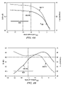
- FIGS. 10A and 10B are plots comparing EVM and ACLR1, respectively, performance with adaptive gain/phase normalization as opposed to static normalization. As illustrated, gain variation up to +/ ⁇ 20 dB are accommodated, with an accuracy better than 0.1 dB. Phase correction accuracy across the dynamic range is better than 5 degrees.
- R ⁇ a 1 ⁇ X + b 1 ⁇ Y 0 ⁇ ⁇ ⁇ ⁇ B a 2 ⁇ X + b 2 ⁇ Y ⁇ B ⁇ ⁇ ⁇ ⁇ 4
- ⁇ is the angle of X+jY, which is between 0 and ⁇ /4.
- method 1 to method 9 can be implemented without a multiply, using only shifters and adders. Methods 10 to 13 require multiplications.
- FIG. 11 is a block diagram illustrating a module to determine approximate amplitude for indexing the predistortion look-up tables. It is an embodiment of method 9 from Table 1. It can be implemented with nine shift operations, six additions and two multiplexers.
- FIG. 12 is a block diagram of mobile cellular phone 1000 for use in the network of FIG. 1 .
- Digital baseband (DBB) unit 1002 can include a digital processing processor system (DSP) that includes embedded memory and security features.
- DBB digital baseband
- SP digital processing processor system
- Stimulus Processing (SP) unit 1004 receives a voice data stream from handset microphone 1013 a and sends a voice data stream to handset mono speaker 1013 b .
- SP unit 1004 also receives a voice data stream from microphone 1014 a and sends a voice data stream to mono headset 1014 b .
- SP and DBB are separate ICs.
- SP does not embed a programmable processor core, but performs processing based on configuration of audio paths, filters, gains, etc being setup by software running on the DBB.
- SP processing is performed on the same processor that performs DBB processing.
- a separate DSP or other type of processor performs SP processing.
- RF transceiver 1006 is a digital radio processor as and includes a receiver for receiving a stream of coded data frames from a cellular base station via antenna 1007 and a transmitter for transmitting a stream of coded data frames to the cellular base station via antenna 1007 .
- DCO digitally controlled oscillator
- Fine frequency resolution is achieved through high-speed dithering of its varactors.
- Digital logic built around the DCO realizes an interpolative all-digital PLL (ADPLL) that is used as a local oscillator for both the transmitter and receiver and operates as described above.
- ADPLL interpolative all-digital PLL
- the Cartesian transmitter architecture utilizes the wideband direct frequency modulation capability of the ADPLL and a digitally controlled power amplifier (DPA) for the power ramp and amplitude modulation.
- DPA digitally controlled power amplifier
- a single transceiver supports both GSM and WCDMA operation but other embodiments may use multiple transceivers for different transmission standards. Other embodiments may have transceivers for a later developed transmission standard with appropriate configuration.
- RF transceiver 1006 is connected to DBB 1002 which provides processing of the frames of encoded data being received and transmitted by cell phone 1000 .
- the basic WCDMA DSP radio consists of control and data channels, rake energy correlations, path selection, rake decoding, and radio feedback. Interference estimation and path selection is performed by instructions stored in memory 1012 and executed by DBB 1002 in response to signals received by transceiver 1006 . Programmable features of the ADPLL within transceiver 1006 are controlled by instructions executed by DBB 1002 .
- Transceiver 1006 includes an embodiment of the present invention to perform adaptive gain/phase normalization and adaptive complex gain predistortion, as described in more detail above.
- a least means squared (LMS) based adaptation technique is used for a complex gain lookup table (LUT) to track the temperature variations of the transmitter's nonlinear characteristics during operation.
- the algorithm is optimized to enable a low complexity hardware implementation and provides relatively fast convergence.
- An amplitude approximation method that is suitable to address the complex gain LUT is embodied that avoids the computation of square root.
- an adaptive loop gain/phase normalization technique is embodied that avoids the appearance of curve discontinuities and maintains the accuracy of open loop power control. It reuses the existing LUT adaptation hardware and therefore is inexpensive to implement.
- DBB unit 1002 may send or receive data to various devices connected to universal serial bus (USB) port 1026 .
- DBB 1002 can be connected to subscriber identity module (SIM) card 1010 and stores and retrieves information used for making calls via the cellular system.
- SIM subscriber identity module
- DBB 1002 can also connected to memory 1012 that augments the onboard memory and is used for various processing needs.
- DBB 1002 can be connected to Bluetooth baseband unit 1030 for wireless connection to a microphone 1032 a and headset 1032 b for sending and receiving voice data.
- DBB 1002 can also be connected to display 1020 and can send information to it for interaction with a user of the mobile UE 1000 during a call process.
- Display 1020 may also display pictures received from the network, from a local camera 1028 , or from other sources such as USB 1026 .
- DBB 1002 may also send a video stream to display 1020 that is received from various sources such as the cellular network via RF transceiver 1006 or camera 1028 .
- DBB 1002 may also send a video stream to an external video display unit via encoder 1022 over composite output terminal 1024 .
- Encoder unit 1022 can provide encoding according to PAL/SECAM/NTSC video standards.
- audio codec 1009 receives an audio stream from FM Radio tuner 1008 and sends an audio stream to stereo headset 1016 and/or stereo speakers 1018 .
- there may be other sources of an audio stream such a compact disc (CD) player, a solid state memory module, etc.
- desktop equipment and other stationary equipment being served by a cellular network may also embody an ADPLL as described herein.
- DSPs Digital Signal Processors
- ASIC Application Specific Integrated Circuit
- An ASIC may contain one or more megacells which each include custom designed functional circuits combined with pre-designed functional circuits provided by a design library.
- An embodiment of the invention may include a system with a processor coupled to a computer readable medium in which a software program is stored that contains instructions that when executed by the processor perform the functions of modules and circuits described herein.
- the computer readable medium may be memory storage such as dynamic random access memory (DRAM), static RAM (SRAM), read only memory (ROM), Programmable ROM (PROM), erasable PROM (EPROM) or other similar types of memory.
- the computer readable media may also be in the form of magnetic, optical, semiconductor or other types of discs or other portable memory devices that can be used to distribute the software for downloading to a system for execution by a processor.
- the computer readable media may also be in the form of magnetic, optical, semiconductor or other types of disc unit coupled to a system that can store the software for downloading or for direct execution by a processor.
- the terms “applied,” “connected,” and “connection” mean electrically connected, including where additional elements may be in the electrical connection path.
- Associated means a controlling relationship, such as a memory resource that is controlled by an associated port.
- assert, assertion, de-assert, de-assertion, negate and negation are used to avoid confusion when dealing with a mixture of active high and active low signals. Assert and assertion are used to indicate that a signal is rendered active, or logically true. De-assert, de-assertion, negate, and negation are used to indicate that a signal is rendered inactive, or logically false.
Landscapes
- Engineering & Computer Science (AREA)
- Power Engineering (AREA)
- Physics & Mathematics (AREA)
- Nonlinear Science (AREA)
- Amplifiers (AREA)
Abstract
Description
√{square root over (I 2 +Q 2)}
The parameter K is the desired gain of the linearized transmitter.
εk =Z−LUT[n]×{tilde over (Y)}
E(|εk|2)≈(Z−{tilde over (Y)}×LUT[n])×(Z−{tilde over (Y)}×LUT[n])*
where:
LUT[n] indicates an entry in the second compensation lookup table,
{tilde over (Y)}* is a complex conjugate value of the normalized feedback signal {tilde over (Y)}.
εk is an error signal corresponding to a difference between pre-distorted signal Z and post-distorted signal Zfb; and
μ is an update factor (real-valued) that controls the speed of convergence.
εk =Z−LUT[n]×Y
εk=(I p +jQ p)−LUT[n]×(I o +jQ o)
LUT[n]=LUT[n]+δ G
δG=εk×(I o −jQ o)×μk
where k is the quadrant number containing the vector (Io+jQo).
εk=(I p +jQ p)−LUTi×(I o +jQ o)
Where LUTi is given by:
LUTi=LUT[n]+interp_factor×(LUT[n+1]−LUT[n])
LUT[n]=LUT[n]+(1−interp_factor)×δG
LUT[n+1]=LUT[n+1]+interp_factor×δG
where k is the quadrant number containing a vector (Io+jQo) corresponding to normalized feedback signal {tilde over (Y)}, and
μ is an update factor (real-valued) that controls the speed of convergence.
Adaptive Loop Gain Normalization
-
- The system can only provide an estimate of the overall loop gain
- The gains of different components in feedback loop vary with temperature. The predistorter adaptation will try to compensate for the linear gain variations (as opposed to just nonlinear components), causing the LUT curve to move up and down. This will create curve discontinuities since the updates are only local.
- In addition to creating discontinuities when the linear component of the predistortion curve varies, the accuracy of open-loop power control will be severely degraded.
- A complex adaptive gain normalization block is chosen to also remove phase shifts that could be due to changes in matching conditions etc. . . . Those phase shifts could also cause temporary discontinuities in real and imaginary LUT curves because of the local nature of the update.
I p +jQ p=α×(I o +jQ o),
over the linear code region only, such as
e k=(I p +jQ p)−αk*(I o +jQ o)
where (Ip+jQp) is the feed forward signal and (Io+jQo) is the feedback signal.
e k+1 =e k+μ×(I O −jQ O)
where μ is an update factor (real-valued) that controls the speed of convergence.
X=max(|I|,|Q|)
Y=min(|I|,|Q|)
where θ is the angle of X+jY, which is between 0 and π/4.
| TABLE 1 |
| Parameters for 13 linear magnitude approximations |
| Method# | a1 | b1 | tan (θB) | a2 | |
| 1 | 1 | 0 | 1 | — | — |
| 2 | 1 | 1 | 1 | — | — |
| 3 | 1 | 1/2 | 1 | — | — |
| 4 | 1 | 1/4 | 1 | — | — |
| 5 | 1 | 3/8 | 1 | — | — |
| 6 | 31/32 | 3/8 | 1 | — | — |
| 7 | 1 | 0 | 1/4 | 7/8 | 1/2 |
| 8 | 1 | 1/4 | 1/2 | 3/4 | 3/4 |
| 9 | 1 | 1/8 | 11/29 | 53/64 | 37/64 |
| 10 | 0.94800 | 0.39300 | 1 | — | — |
| 11 | 0.96043 | 0.39782 | 1 | — | — |
| 12 | 0.98644 | 0.23287 | 1/2 | 0.81651 | 0.58851 |
| 13 | 0.99030 | 0.19698 | tan (π/8) | 0.83954 | 0.56094 |
Claims (20)
X=max(|I|,|Q|)
Y=min(|I|,|Q|)
LUT[n]=LUT[n]+δ G
X=max(|I|,|Q|)
Y=min(|I|,|Q|)
LUT[n]=LUT[n]+δ G
Priority Applications (1)
| Application Number | Priority Date | Filing Date | Title |
|---|---|---|---|
| US12/413,109 US8055217B2 (en) | 2008-08-05 | 2009-03-27 | Adaptive complex gain predistorter for a transmitter |
Applications Claiming Priority (2)
| Application Number | Priority Date | Filing Date | Title |
|---|---|---|---|
| US8626108P | 2008-08-05 | 2008-08-05 | |
| US12/413,109 US8055217B2 (en) | 2008-08-05 | 2009-03-27 | Adaptive complex gain predistorter for a transmitter |
Publications (2)
| Publication Number | Publication Date |
|---|---|
| US20100035554A1 US20100035554A1 (en) | 2010-02-11 |
| US8055217B2 true US8055217B2 (en) | 2011-11-08 |
Family
ID=41653392
Family Applications (1)
| Application Number | Title | Priority Date | Filing Date |
|---|---|---|---|
| US12/413,109 Active 2030-07-23 US8055217B2 (en) | 2008-08-05 | 2009-03-27 | Adaptive complex gain predistorter for a transmitter |
Country Status (1)
| Country | Link |
|---|---|
| US (1) | US8055217B2 (en) |
Cited By (13)
| Publication number | Priority date | Publication date | Assignee | Title |
|---|---|---|---|---|
| US20100271123A1 (en) * | 2009-04-27 | 2010-10-28 | Qualcomm Incorporated | Adaptive digital predistortion of complex modulated waveform using localized peak feedback from the output of a power amplifier |
| US20120002752A1 (en) * | 2010-06-30 | 2012-01-05 | Qualcomm Incorporated | Predistortion of complex modulated waveform |
| US20120007672A1 (en) * | 2009-12-23 | 2012-01-12 | Universite De Nantes | Linearization Device for a Power Amplifier |
| US20120098596A1 (en) * | 2010-10-21 | 2012-04-26 | Fujitsu Limited | Power amplifier apparatus, distortion compensation coefficient updating method, and transmission apparatus |
| US20120108189A1 (en) * | 2010-11-02 | 2012-05-03 | Crestcom, Inc. | Transmitter Linearized Using Bias Deviation Gain Adjustment And Method Therefor |
| US20120264378A1 (en) * | 2011-04-15 | 2012-10-18 | Qualcomm Incorporated | Methods and apparatus for power amplifier calibration |
| US8340602B1 (en) * | 2009-10-16 | 2012-12-25 | Qualcomm Incorporated | Power amplifier linearization system and method |
| US20130188671A1 (en) * | 2012-01-20 | 2013-07-25 | Research In Motion Limited | Mobile wireless communications device with impedance matching and related methods |
| US8964821B2 (en) | 2011-10-14 | 2015-02-24 | Qualcomm Incorporated | Shared feedback for adaptive transmitter pre-distortion |
| US8976896B2 (en) | 2010-11-02 | 2015-03-10 | Crestcom, Inc. | Transmitter linearized in response to derivative signal and method therefor |
| US8989307B2 (en) | 2013-03-05 | 2015-03-24 | Qualcomm Incorporated | Power amplifier system including a composite digital predistorter |
| US9595924B2 (en) | 2012-08-03 | 2017-03-14 | Broadcom Corporation | Calibration for power amplifier predistortion |
| CN106941466A (en) * | 2016-01-04 | 2017-07-11 | 中兴通讯股份有限公司 | A kind of method and device of the digital pre-distortion of software-hardware synergism |
Families Citing this family (32)
| Publication number | Priority date | Publication date | Assignee | Title |
|---|---|---|---|---|
| US8411709B1 (en) | 2006-11-27 | 2013-04-02 | Marvell International Ltd. | Use of previously buffered state information to decode in an hybrid automatic repeat request (H-ARQ) transmission mode |
| US8131218B2 (en) | 2007-04-13 | 2012-03-06 | General Dynamics C4 Systems, Inc. | Methods and apparatus for wirelessly communicating signals that include embedded synchronization/pilot sequences |
| US8897393B1 (en) | 2007-10-16 | 2014-11-25 | Marvell International Ltd. | Protected codebook selection at receiver for transmit beamforming |
| US8542725B1 (en) | 2007-11-14 | 2013-09-24 | Marvell International Ltd. | Decision feedback equalization for signals having unequally distributed patterns |
| US8565325B1 (en) | 2008-03-18 | 2013-10-22 | Marvell International Ltd. | Wireless device communication in the 60GHz band |
| US8379752B2 (en) * | 2008-03-19 | 2013-02-19 | General Dynamics C4 Systems, Inc. | Methods and apparatus for multiple-antenna communication of wireless signals with embedded synchronization/pilot sequences |
| US8331420B2 (en) * | 2008-04-14 | 2012-12-11 | General Dynamics C4 Systems, Inc. | Methods and apparatus for multiple-antenna communication of wireless signals with embedded pilot signals |
| US8761261B1 (en) | 2008-07-29 | 2014-06-24 | Marvell International Ltd. | Encoding using motion vectors |
| US8498342B1 (en) | 2008-07-29 | 2013-07-30 | Marvell International Ltd. | Deblocking filtering |
| US8345533B1 (en) | 2008-08-18 | 2013-01-01 | Marvell International Ltd. | Frame synchronization techniques |
| US8681893B1 (en) | 2008-10-08 | 2014-03-25 | Marvell International Ltd. | Generating pulses using a look-up table |
| US8520771B1 (en) * | 2009-04-29 | 2013-08-27 | Marvell International Ltd. | WCDMA modulation |
| EP2290811A1 (en) * | 2009-08-05 | 2011-03-02 | STmicroelectronics SA | Digital predistorter for variable supply amplifier |
| US20110069749A1 (en) * | 2009-09-24 | 2011-03-24 | Qualcomm Incorporated | Nonlinear equalizer to correct for memory effects of a transmitter |
| US8744009B2 (en) * | 2009-09-25 | 2014-06-03 | General Dynamics C4 Systems, Inc. | Reducing transmitter-to-receiver non-linear distortion at a transmitter prior to estimating and cancelling known non-linear distortion at a receiver |
| US8355466B2 (en) * | 2009-09-25 | 2013-01-15 | General Dynamics C4 Systems, Inc. | Cancelling non-linear power amplifier induced distortion from a received signal by moving incorrectly estimated constellation points |
| US8326239B1 (en) * | 2009-10-16 | 2012-12-04 | Qualcomm Atheros, Inc. | Power amplifier linearization using digital predistortion |
| US20110141930A1 (en) * | 2009-12-11 | 2011-06-16 | Qualcomm Incorporated | Baseband compensation for phase discontinuities in radio frequency communication devices |
| US20110250853A1 (en) * | 2010-04-09 | 2011-10-13 | Andrea Camuffo | Operating point setting of an amplifier |
| US8565343B1 (en) | 2010-06-29 | 2013-10-22 | Qualcomm Incorporated | Transmit power control utilizing loopback error vector magnitude thresholds |
| US8817771B1 (en) | 2010-07-16 | 2014-08-26 | Marvell International Ltd. | Method and apparatus for detecting a boundary of a data frame in a communication network |
| JP5663261B2 (en) * | 2010-10-26 | 2015-02-04 | 日本無線株式会社 | Predistorter |
| JP5605184B2 (en) * | 2010-11-18 | 2014-10-15 | 富士通株式会社 | Frequency shift circuit and communication device |
| US20120195392A1 (en) * | 2011-02-02 | 2012-08-02 | Provigent Ltd. | Predistortion in split-mount wireless communication systems |
| US8553610B2 (en) | 2011-05-12 | 2013-10-08 | Qualcomm Incorporated | Interference cancellation repeater incorporating a non-linear element |
| JP6064714B2 (en) * | 2013-03-19 | 2017-01-25 | 富士通株式会社 | Distortion compensation apparatus and distortion compensation method |
| KR102201566B1 (en) * | 2017-08-18 | 2021-01-11 | 주식회사 엘지화학 | Customized bms module and method for designing thereof |
| TWI661740B (en) * | 2017-12-01 | 2019-06-01 | 財團法人工業技術研究院 | Multi-cell coordination system and method |
| WO2019233555A1 (en) | 2018-06-05 | 2019-12-12 | Telefonaktiebolaget Lm Ericsson (Publ) | Digital predistortion low power implementation |
| WO2019233558A1 (en) | 2018-06-05 | 2019-12-12 | Telefonaktiebolaget Lm Ericsson (Publ) | Low-power approximate dpd actuator for 5g-new radio |
| CN115987729B (en) * | 2022-06-24 | 2023-09-29 | 上海星思半导体有限责任公司 | Phase alignment method, phase alignment device and computer-readable storage medium |
| CN120595240A (en) * | 2023-06-14 | 2025-09-05 | 加特兰微电子科技(上海)有限公司 | Received signal compensation method, device, integrated circuit and radio device |
Citations (3)
| Publication number | Priority date | Publication date | Assignee | Title |
|---|---|---|---|---|
| US7251290B2 (en) * | 2002-12-16 | 2007-07-31 | Nortel Networks Limited | Adaptive controller for linearization of transmitter |
| US20090054016A1 (en) * | 2007-08-21 | 2009-02-26 | Texas Instruments Incorporated | Apparatus and Method for Adaptive Cartesian Transmitter Linearization and Wireless Transmitter Employing the Same |
| US20090051426A1 (en) * | 2007-08-21 | 2009-02-26 | Texas Instruments Incorporated | Large-Dynamic-Range Lookup Table for a Transmitter Predistorter and System and Method Employing the Same |
-
2009
- 2009-03-27 US US12/413,109 patent/US8055217B2/en active Active
Patent Citations (3)
| Publication number | Priority date | Publication date | Assignee | Title |
|---|---|---|---|---|
| US7251290B2 (en) * | 2002-12-16 | 2007-07-31 | Nortel Networks Limited | Adaptive controller for linearization of transmitter |
| US20090054016A1 (en) * | 2007-08-21 | 2009-02-26 | Texas Instruments Incorporated | Apparatus and Method for Adaptive Cartesian Transmitter Linearization and Wireless Transmitter Employing the Same |
| US20090051426A1 (en) * | 2007-08-21 | 2009-02-26 | Texas Instruments Incorporated | Large-Dynamic-Range Lookup Table for a Transmitter Predistorter and System and Method Employing the Same |
Non-Patent Citations (10)
| Title |
|---|
| "A Baker's Dozen Magnitude Approximations and Their Detection Statistics", IEEE Transactions on Aerospace and Electronic Systems, vol. AES-12, vo. 1, Jan. 1976, pp. 86-89. |
| H. Bcsbcs et al., "A Fast Adaptive Polynomial Predistorter for Power Amplifiers", 2001 IEEE, pp. 659-663. |
| Ilari Teikari et al., "Baseband Digital Predistorter with Quadrature Error Correction", 2004 IEEE, pp. 159-162. |
| James K. Cavers, "Amplifier Linearization Using a Digital Predistorter with Fast Adaptation and Low Memory Requirements", IEEE Transactions on Vehicular Technology, vol. 39, No. 4, Nov. 1990, pp. 374-382. |
| James K. Cavers, "Optimum Table Spacing in Predistorting Amplifier Linearizers", IEEE Transactions on Vehicular Technology, vol. 48, No. 5, Sep. 1999, pp. 1699-1705. |
| John Homer et al., "Quantifying the Effects of Dimension on the Convergence Rate of the LMS Adaptive FIR Estimator", IEEE Transactions on Signal Processing, vol. 46, No. 10, Oct. 1998, pp. 2611-2615. |
| Khurram Waheed and Seydou N. Ba, "Adaptive Digital Linearization of a DRP based EDGE Transmitter for Cellular Handsets", IEEE MWSCAS/NEWCAS Conference, Aug. 2007, Montreal, Canada, pp. 706-709. |
| Lars Sundstrom et al., "Quantization Analysis and Design of a Digital Predistortion Linearizer for RF Power Amplifiers", IEEE Transactions on Vehicular Technology, vol. 45, No. 4, Nov. 1996, pp. 707-719. |
| Michael Faulkner and Mats Johansson, "Adaptive Linearization Using Predistortion-Experimental Results", IEEE Transactions on Vehicular Technology, vol. 43, No. 2, May 1994, pp. 323-332. |
| Sung Won Chung et al., "Open-Loop Digital Predistortion Using Cartesian Feedback for Adaptive RF Power Amplifier Linearization", 2001 IEEE, pp. 1449-1452. |
Cited By (20)
| Publication number | Priority date | Publication date | Assignee | Title |
|---|---|---|---|---|
| US20100271123A1 (en) * | 2009-04-27 | 2010-10-28 | Qualcomm Incorporated | Adaptive digital predistortion of complex modulated waveform using localized peak feedback from the output of a power amplifier |
| US8340602B1 (en) * | 2009-10-16 | 2012-12-25 | Qualcomm Incorporated | Power amplifier linearization system and method |
| US20120007672A1 (en) * | 2009-12-23 | 2012-01-12 | Universite De Nantes | Linearization Device for a Power Amplifier |
| US8432220B2 (en) * | 2009-12-23 | 2013-04-30 | Thales | Linearization device for a power amplifier |
| US8737526B2 (en) * | 2010-06-30 | 2014-05-27 | Qualcomm Incorporated | Predistortion of complex modulated waveform |
| US20120002752A1 (en) * | 2010-06-30 | 2012-01-05 | Qualcomm Incorporated | Predistortion of complex modulated waveform |
| US20120098596A1 (en) * | 2010-10-21 | 2012-04-26 | Fujitsu Limited | Power amplifier apparatus, distortion compensation coefficient updating method, and transmission apparatus |
| US8933752B2 (en) * | 2010-10-21 | 2015-01-13 | Fujitsu Limited | Power amplifier apparatus, distortion compensation coefficient updating method, and transmission apparatus |
| US20120108189A1 (en) * | 2010-11-02 | 2012-05-03 | Crestcom, Inc. | Transmitter Linearized Using Bias Deviation Gain Adjustment And Method Therefor |
| US8976896B2 (en) | 2010-11-02 | 2015-03-10 | Crestcom, Inc. | Transmitter linearized in response to derivative signal and method therefor |
| US8489047B2 (en) * | 2010-11-02 | 2013-07-16 | Crestcom, Inc. | Transmitter linearized using bias deviation gain adjustment and method therefor |
| US8712339B2 (en) * | 2011-04-15 | 2014-04-29 | Qualcomm Incorporated | Methods and apparatus for power amplifier calibration |
| US20120264378A1 (en) * | 2011-04-15 | 2012-10-18 | Qualcomm Incorporated | Methods and apparatus for power amplifier calibration |
| US8964821B2 (en) | 2011-10-14 | 2015-02-24 | Qualcomm Incorporated | Shared feedback for adaptive transmitter pre-distortion |
| US20130188671A1 (en) * | 2012-01-20 | 2013-07-25 | Research In Motion Limited | Mobile wireless communications device with impedance matching and related methods |
| US9106190B2 (en) * | 2012-01-20 | 2015-08-11 | Blackberry Limited | Mobile wireless communications device with impedance matching and related methods |
| US9595924B2 (en) | 2012-08-03 | 2017-03-14 | Broadcom Corporation | Calibration for power amplifier predistortion |
| US8989307B2 (en) | 2013-03-05 | 2015-03-24 | Qualcomm Incorporated | Power amplifier system including a composite digital predistorter |
| CN106941466A (en) * | 2016-01-04 | 2017-07-11 | 中兴通讯股份有限公司 | A kind of method and device of the digital pre-distortion of software-hardware synergism |
| CN106941466B (en) * | 2016-01-04 | 2020-11-06 | 中兴通讯股份有限公司 | A method and device for digital predistortion of software and hardware cooperation |
Also Published As
| Publication number | Publication date |
|---|---|
| US20100035554A1 (en) | 2010-02-11 |
Similar Documents
| Publication | Publication Date | Title |
|---|---|---|
| US8055217B2 (en) | Adaptive complex gain predistorter for a transmitter | |
| US20200358640A1 (en) | Modulation agnostic digital hybrid mode power amplifier system and method | |
| US7915954B2 (en) | Amplifier predistortion and autocalibration method and apparatus | |
| US9634695B1 (en) | Wireless devices having multiple transmit chains with predistortion circuitry | |
| US20210314210A1 (en) | System and method for digital memorized predistortion for wireless communication | |
| US7403573B2 (en) | Uncorrelated adaptive predistorter | |
| JP5864176B2 (en) | System and method for spurious radiation cancellation | |
| JP4951238B2 (en) | Polar coordinate modulation transmission apparatus, adaptive distortion compensation processing system, polar modulation transmission method, and adaptive distortion compensation processing method | |
| US8150335B2 (en) | Apparatus and method for adaptive cartesian transmitter linearization and wireless transmitter employing the same | |
| US20080139141A1 (en) | Method and system for estimating and compensating non-linear distortion in a transmitter using data signal feedback | |
| US20050017801A1 (en) | Elimination of peak clipping and improved efficiency for RF power amplifiers with a predistorter | |
| US20050180526A1 (en) | Predistortion apparatus and method for compensating for a nonlinear distortion characteristic of a power amplifier using a look-up table | |
| US20080290939A1 (en) | Method and apparatus for distortion correction of RF amplifiers | |
| Mehta et al. | An efficient linearization scheme for a digital polar EDGE transmitter | |
| US20100271124A1 (en) | Distortion Compensation Device | |
| KR20050083865A (en) | A method and system for broadband predistortion linearization | |
| Berland et al. | Digital signal processing techniques to compensate for RF imperfections in advanced transmitter architectures | |
| Tango et al. | Simplified Temperature Compensation Technique for Digital Predistorter Using Fixed Coefficients | |
| HK1228604A1 (en) | Modulation agnostic digital hybrid mode power amplifier system and method | |
| HK1228604A (en) | Modulation agnostic digital hybrid mode power amplifier system and method | |
| KR20180004314A (en) | Modulation agnostic digital hybrid mode power amplifier system and method |
Legal Events
| Date | Code | Title | Description |
|---|---|---|---|
| AS | Assignment |
Owner name: TEXAS INSTRUMENTS INCORPORATED,TEXAS Free format text: ASSIGNMENT OF ASSIGNORS INTEREST;ASSIGNORS:BA, SEYDOU NOUROU;WAHEED, KHURRAM;REEL/FRAME:022465/0488 Effective date: 20090327 Owner name: TEXAS INSTRUMENTS INCORPORATED, TEXAS Free format text: ASSIGNMENT OF ASSIGNORS INTEREST;ASSIGNORS:BA, SEYDOU NOUROU;WAHEED, KHURRAM;REEL/FRAME:022465/0488 Effective date: 20090327 |
|
| STCF | Information on status: patent grant |
Free format text: PATENTED CASE |
|
| FPAY | Fee payment |
Year of fee payment: 4 |
|
| MAFP | Maintenance fee payment |
Free format text: PAYMENT OF MAINTENANCE FEE, 8TH YEAR, LARGE ENTITY (ORIGINAL EVENT CODE: M1552); ENTITY STATUS OF PATENT OWNER: LARGE ENTITY Year of fee payment: 8 |
|
| MAFP | Maintenance fee payment |
Free format text: PAYMENT OF MAINTENANCE FEE, 12TH YEAR, LARGE ENTITY (ORIGINAL EVENT CODE: M1553); ENTITY STATUS OF PATENT OWNER: LARGE ENTITY Year of fee payment: 12 |