US8053713B2 - Light source device and light amount correcting method to perform light amount corection corresponding to a change in a light source characteristic - Google Patents
Light source device and light amount correcting method to perform light amount corection corresponding to a change in a light source characteristic Download PDFInfo
- Publication number
- US8053713B2 US8053713B2 US12/363,121 US36312109A US8053713B2 US 8053713 B2 US8053713 B2 US 8053713B2 US 36312109 A US36312109 A US 36312109A US 8053713 B2 US8053713 B2 US 8053713B2
- Authority
- US
- United States
- Prior art keywords
- light
- value
- amount
- light amount
- current
- Prior art date
- Legal status (The legal status is an assumption and is not a legal conclusion. Google has not performed a legal analysis and makes no representation as to the accuracy of the status listed.)
- Expired - Fee Related, expires
Links
- 238000000034 method Methods 0.000 title claims description 21
- 239000004065 semiconductor Substances 0.000 claims abstract description 48
- 230000003287 optical effect Effects 0.000 claims abstract description 43
- 238000004364 calculation method Methods 0.000 claims description 3
- 238000012937 correction Methods 0.000 description 63
- 238000012545 processing Methods 0.000 description 28
- 238000010586 diagram Methods 0.000 description 22
- 238000006243 chemical reaction Methods 0.000 description 16
- 238000012986 modification Methods 0.000 description 13
- 230000004048 modification Effects 0.000 description 13
- 239000003086 colorant Substances 0.000 description 12
- 238000005259 measurement Methods 0.000 description 10
- 238000001514 detection method Methods 0.000 description 6
- 230000006870 function Effects 0.000 description 6
- 230000007423 decrease Effects 0.000 description 3
- 230000006866 deterioration Effects 0.000 description 3
- 230000001131 transforming effect Effects 0.000 description 3
- NAWXUBYGYWOOIX-SFHVURJKSA-N (2s)-2-[[4-[2-(2,4-diaminoquinazolin-6-yl)ethyl]benzoyl]amino]-4-methylidenepentanedioic acid Chemical compound C1=CC2=NC(N)=NC(N)=C2C=C1CCC1=CC=C(C(=O)N[C@@H](CC(=C)C(O)=O)C(O)=O)C=C1 NAWXUBYGYWOOIX-SFHVURJKSA-N 0.000 description 2
- 238000012935 Averaging Methods 0.000 description 2
- 230000000052 comparative effect Effects 0.000 description 2
- 238000004590 computer program Methods 0.000 description 2
- 230000003247 decreasing effect Effects 0.000 description 2
- 238000011156 evaluation Methods 0.000 description 2
- 238000002945 steepest descent method Methods 0.000 description 2
- 230000005540 biological transmission Effects 0.000 description 1
- 230000000694 effects Effects 0.000 description 1
- 230000010354 integration Effects 0.000 description 1
- 230000001678 irradiating effect Effects 0.000 description 1
- 239000004973 liquid crystal related substance Substances 0.000 description 1
- 239000000463 material Substances 0.000 description 1
- 229910044991 metal oxide Inorganic materials 0.000 description 1
- 150000004706 metal oxides Chemical class 0.000 description 1
- 229910052710 silicon Inorganic materials 0.000 description 1
- 239000010703 silicon Substances 0.000 description 1
Images


Classifications
-
- G—PHYSICS
- G01—MEASURING; TESTING
- G01J—MEASUREMENT OF INTENSITY, VELOCITY, SPECTRAL CONTENT, POLARISATION, PHASE OR PULSE CHARACTERISTICS OF INFRARED, VISIBLE OR ULTRAVIOLET LIGHT; COLORIMETRY; RADIATION PYROMETRY
- G01J1/00—Photometry, e.g. photographic exposure meter
- G01J1/10—Photometry, e.g. photographic exposure meter by comparison with reference light or electric value provisionally void
- G01J1/20—Photometry, e.g. photographic exposure meter by comparison with reference light or electric value provisionally void intensity of the measured or reference value being varied to equalise their effects at the detectors, e.g. by varying incidence angle
- G01J1/28—Photometry, e.g. photographic exposure meter by comparison with reference light or electric value provisionally void intensity of the measured or reference value being varied to equalise their effects at the detectors, e.g. by varying incidence angle using variation of intensity or distance of source
- G01J1/30—Photometry, e.g. photographic exposure meter by comparison with reference light or electric value provisionally void intensity of the measured or reference value being varied to equalise their effects at the detectors, e.g. by varying incidence angle using variation of intensity or distance of source using electric radiation detectors
- G01J1/32—Photometry, e.g. photographic exposure meter by comparison with reference light or electric value provisionally void intensity of the measured or reference value being varied to equalise their effects at the detectors, e.g. by varying incidence angle using variation of intensity or distance of source using electric radiation detectors adapted for automatic variation of the measured or reference value
-
- H—ELECTRICITY
- H05—ELECTRIC TECHNIQUES NOT OTHERWISE PROVIDED FOR
- H05B—ELECTRIC HEATING; ELECTRIC LIGHT SOURCES NOT OTHERWISE PROVIDED FOR; CIRCUIT ARRANGEMENTS FOR ELECTRIC LIGHT SOURCES, IN GENERAL
- H05B45/00—Circuit arrangements for operating light-emitting diodes [LED]
- H05B45/10—Controlling the intensity of the light
- H05B45/12—Controlling the intensity of the light using optical feedback
Definitions
- the present invention relates to a light source device, an image display apparatus, and a light amount correcting method.
- a laser scan display that raster-scans beam-like light such as a laser beam on a projection surface and displays an image attracts attention.
- a laser scan display has characteristics that, for example, contrast is extremely high compared with, for example, a projector employing a liquid crystal light valve because complete black can be represented by stopping supply of the laser beam, color purity is high because the laser beam has single wavelength, and a beam can be easily shaped (narrowed) because coherence is high. Therefore, the laser scan display is promising as a high-quality display that realizes high contrast, high color reproducibility, and high resolution.
- a semiconductor laser element such as a laser diode is mainly used.
- a laser characteristic of such a semiconductor laser element changes because of a temperature change, aged deterioration, and the like. Therefore, it is necessary to correct a laser beam amount such that desired image luminance can be obtained.
- JP-A-7-147446 discloses a technique for changing a bias current value of a semiconductor laser element by two or more points, detecting light emission power of the semiconductor laser element with light-reception-power detecting means, and detecting, for example, a change in quantum efficiency between the bias current value and a threshold current value of the semiconductor laser element to set a DC bias current of the semiconductor laser element in bias-current controlling means and set a pulse current corresponding to the change in the quantum efficiency and the like in pulse-current controlling means to maintain a level of a laser output constant.
- JP-A-2003-91853 discloses a technique for automatically calculating a relational expression between a detected light amount of a laser beam source and a set value of a light output, setting data of this relational expression in a light recording media driving device, and adjusting an output level of the laser beam source.
- An advantage of some aspects of the invention is to provide a light source device that can improve light amount correction accuracy by performing light amount correction corresponding to a change in a light source characteristic on a real time basis, an image display apparatus including the light source device, and a light amount correcting method.
- a light source device including:
- a semiconductor light-emitting element that emits, according to an input value, light having first wavelength
- a wavelength converting element that converts, with a nonlinear optical effect, the light having the first wavelength emitted by the semiconductor light-emitting element into light having second wavelength
- a light-amount measuring unit that measures a light amount of the light having the second wavelength emitted from the wavelength converting element
- an equivalent-light-amount calculating unit that calculates, on the basis of the measured light amount measured by the light-amount measuring unit, an equivalent light amount equivalent to a light amount of the light having the first wavelength
- a light-amount correcting unit that corrects an emitted light amount of the semiconductor light-emitting element using the input value and the equivalent light amount.
- the light source device With the light source device according to the aspect of the invention, it is possible to execute light amount correction for the light having the second wavelength on a real time basis by detecting the light having the second wavelength. Further, it is possible to improve accuracy of the correction.
- the light source device further includes a current supplying unit that supplies a driving current to the semiconductor light-emitting element according to the input value and a command value outputted by the light-amount correcting unit.
- the light-amount correcting unit calculates an equivalent light amount error as a difference between the equivalent light amount and a target equivalent light amount that should be emitted by the semiconductor light-emitting element with respect to the input value, calculates, using an integrated value of a product of the equivalent light amount error and the input value, differential efficiency defined by an amount of change in the equivalent light amount with respect to an amount of change in the driving current, calculates, using an integrated value of the equivalent light amount error, a threshold current value of the semiconductor light-emitting element, and corrects the command value according to the differential efficiency and the threshold current value.
- the differential efficiency as one of light source characteristic parameters is corrected, a threshold of a driving signal as one of the light source characteristic parameters is corrected, and a command value for generating a driving signal having the differential efficiency and the threshold after the correction is outputted to the current supplying unit. Therefore, it is possible to perform, on a real time basis, light amount correction corresponding to a change in the light source characteristic due to a temperature change or the like during operation. Further, it is possible to obtain high light amount correction accuracy.
- the command value includes a gradation current command value corrected according to the differential efficiency and a threshold current command value corrected according to the threshold current value,
- the current supplying unit includes:
- the current supplying unit adds up the gradation current and the threshold current and supplies an added-up current to the light-emitting unit as the driving current
- the light-amount correcting unit calculates a present value of a first variable representing the gradation current command value by subtracting a numerical value proportional to the integrated value of the product of the equivalent light amount error and the input value from the last value of the first variable and calculates a present value of a second variable representing the threshold current command value by subtracting a numerical value proportional to the integrated value of the equivalent light amount error from the last value of the second variable.
- the light source device With the light source device according to the aspect of the invention, it is possible to sequentially calculate a first variable and a second variable for minimizing the equivalent light amount error and correct the differential efficiency and the threshold on the basis of the first variable and the second variable. Therefore, it is possible to perform, on a real time basis, light amount correction corresponding to a change in the light source characteristic due to a temperature change of the like during operation. Further, it is possible to obtain high light amount correction accuracy.
- the light-amount correcting unit uses, as an input value for calculation used in calculating the integrated value of the product of the equivalent light amount error and the input value, an average of the input value, an initially set input value set in advance, or a difference between a median value between a minimum input value and a maximum input value and the input value.
- the light source device even when deviation between the target equivalent light amount and the equivalent light amount occurs to reduce the integrated value of the equivalent light amount error and the integrated value of the product of the equivalent light amount error and the input value to substantially zero, it is possible to prevent the integrated value of the product of the equivalent light amount error and the input value from being reduced to zero. Further, it is possible to prevent the correction operation in the light-amount correcting unit from being stopped.
- the light-amount correcting unit multiplies a value of the product of the equivalent light amount error and the input value with a weighting constant for setting the value smaller as the value is generated further in the past to thereby calculate an integrated value of the product of the equivalent light amount error and the input value.
- the light source device With the light source device according to the aspect of the invention, it is possible to perform light amount correction with nearest measurement data weighted. Further, it is possible to improve light amount correction accuracy.
- the light-amount correcting unit increases the threshold current and reduces the threshold current when a value obtained by subtracting the black level light amount from the equivalent light amount reaches a first set light amount for specifying predetermined brightness, and sets, as an initial value of the threshold current, the threshold current at the time when the value obtained by subtracting the black level light amount from the equivalent light amount reaches a second set light amount regarded as a black level, and outputs a maximum value of the input value to the current supplying unit, increases the gradation current, and sets, as an initial value of the gradation current, the gradation value at the time when the
- the light source device With the light source device according to the aspect of the invention, it is possible to obtain initial values of a gradation current and a threshold current with the corrected offset of the measured light amount of the light-amount measuring unit. Further, it is possible to improve light amount correction accuracy.
- the light-amount correcting unit uses, as the last value of the second variable in calculating a present value of the second variable in the first time, the initial value of the threshold current calculated by the initial setting operation and uses, as the last value of the first variable in calculating a present value of the first variable in the first time, the initial value of the gradation current.
- the light source device With the light source device according to the aspect of the invention, it is possible to accurately calculate the present value of the second variable and the present value of the first variable in the first time. Therefore, it is possible to further improve light amount correction accuracy.
- the invention can be realized in various forms such as a light source device including a semiconductor light-emitting element, a control device and a control method for the semiconductor light-emitting element, an image display apparatus including the light source device, a control device and a control method for the image display apparatus, a computer program for realizing functions of the methods and the devices, and a recording medium having the computer program recorded therein.
- FIG. 1 is a block diagram of a schematic configuration of an image display apparatus.
- FIG. 2 is a schematic diagram of a configuration of a laser scanning unit.
- FIG. 3 is a schematic diagram for explaining a rotation angle of a reflection mirror.
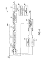
- FIG. 4 is a block diagram of a configuration of a light source device.
- FIG. 5 is a block diagram of a schematic configuration of a red laser driver.
- FIG. 6 is a diagram for explaining a circuit configuration of the red laser driver.
- FIGS. 7A to 7C are diagrams for explaining a relation between a light emission amount of a laser beam source and infrared light emitted by the laser beam source.
- FIG. 8 is a graph of a laser characteristic of a red laser beam source.
- FIGS. 9A to 9E are graphs for explaining a principle of light amount correction performed by a light-amount correcting circuit.
- FIG. 10 is a graph for explaining, as a comparative example, light amount correction performed according to a visible light amount.
- FIG. 11 is a block diagram of an internal configuration of the light-amount correcting circuit.
- FIGS. 12A to 12D are block diagrams of an internal configuration of a part of the light-amount correcting circuit.
- FIGS. 13A to 13D are block diagrams of an internal configuration of a part of the light-amount correcting circuit.
- FIG. 14 is a schematic diagram of a detailed configuration of the light-amount correcting circuit.
- FIG. 15 is a graph for explaining an initial setting operation executed by the light-amount correcting circuit.
- FIG. 16 is a flowchart of the initial setting operation executed by the light amount correcting circuit.
- FIG. 17 is a timing chart of a steady operation of the image display apparatus.
- FIGS. 18A and 18B are graphs for explaining a modification of the image display apparatus.
- FIG. 19 is a diagram for explaining the modification of the image display apparatus.
- FIG. 20 is a diagram for explaining the modification of the image display apparatus.
- FIG. 1 is a block diagram of a configuration of an image display apparatus LDS according to this embodiment.
- the image display apparatus LSD As an example of the image display apparatus LSD, a laser scan display that scans a laser beam on a screen (a projection surface) 200 to display an image is explained.
- the screen 200 is a transmission screen that transmits laser beams LR, LG, and LB scanned by a laser scanning unit 50 explained later.
- the image display apparatus LSD is a rear projection projector.
- a user views a displayed image on a surface on the opposite side of an irradiation surface for the laser beams LR, LG, and LB in the screen 200 .
- the image display apparatus LSD only the surface on the viewing side of the screen 200 is exposed and other components are stored in a housing to eliminate the influence of external light.
- the image display apparatus LSD includes a light source device 100 , a video-signal processing circuit 10 , an optical system for optical axis alignment 40 , a laser scanning unit 50 , a scanning driving unit 60 , an irradiation-position detecting unit 70 , and a pixel-synchronization-clock generating circuit 80 .
- the light source device 100 includes laser drivers 20 R, 20 G, and 20 B for respective display lights (red, green, and blue), laser beam sources 30 R, 30 G, and 30 B for the respective colors, a photoelectric conversion element 90 , an I/V converter 91 , an analog square root circuit 99 , an A/D converter 92 , a light-amount correcting circuit 93 , and two D/A converters 94 and 95 .
- a correction system circuit block including the photoelectric conversion element 90 , the I/V converter 91 , the A/D converter 92 , the light-amount correcting circuit 93 , and the D/A converters 94 and 95 is provided to correspond to each of the red laser driver 20 R, the green laser driver 20 G, and the blue laser driver 20 B (i.e., correspond to each of the colors).
- the red laser driver 20 R the green laser driver 20 G
- the blue laser driver 20 B i.e., correspond to each of the colors.
- FIG. 1 for convenience of illustration, only the correction system circuit block corresponding to the red laser driver 20 R is shown as a representative one.
- the video-signal processing circuit 10 receives, as inputs, video signals and synchronization signals (a vertical synchronization signal Vsync and a horizontal synchronization signal Hsync) transmitted from an image supply apparatus (not shown) on the outside such as a notebook personal computer, generates, on the basis of the video signals and the synchronization signals, digital gradation data for specifying gradation values corresponding to respective pixels of an image that should be displayed, and stores the digital gradation data in an internal memory in units of one frame.
- the number of bits N of the digital gradation data is set to four.
- the image display apparatus LSD can perform image display of sixteen gradations (4096 colors) from “0” to “15”.
- the video-signal processing circuit 10 reads out the digital gradation data stored in the internal memory on the basis of a pulse-like frame timing signal Ft for specifying the start of one frame and a pulse-like scanning timing signal St for specifying the start and the end of one horizontal scanning period.
- the pulse-like frame timing signal Ft and the pulse-like scanning timing signal St are inputted from the irradiation-position detecting unit 70 .
- the video-signal processing circuit 10 outputs, in synchronization with a pulse-like pixel synchronization clock signal CL for specifying irradiation timing of laser beams corresponding to the respective pixels in one horizontal scanning period, the digital gradation data of the pixel corresponding to an irradiation position of the laser beam to the light source device 100 .
- the pulse-like pixel synchronization clock signal CL is inputted from the pixel-synchronization-clock generating circuit 80 . More specifically, when the pixel corresponding to the irradiation position of the laser beam is a pixel for red, the video-signal processing circuit 10 outputs red gradation data DR for the red pixel to the red laser driver 20 R. When the pixel corresponding to the irradiation position of the laser beam is a pixel for green, the video-signal processing circuit 10 outputs green gradation data DG for the green pixel to the green laser driver 20 G.
- the video-signal processing circuit 10 When the pixel corresponding to the irradiation position of the laser beam is a pixel for blue, the video-signal processing circuit 10 outputs blue gradation data DB for the blue pixel to the blue laser driver 20 B.
- the video-signal processing circuit 10 outputs the red gradation data DR to the light-amount correcting circuit 93 of the correction system circuit block for red, outputs the green gradation data DG to a light-amount correcting circuit (not shown) of a correction system circuit block for green, and outputs the blue gradation data DB to a light-amount correcting circuit (not shown) of a correction system circuit block for blue.
- the light source device 100 receives the gradation data DR, DG, and DB from the video-signal processing circuit 10 .
- the light source device 100 emits laser beams LR, LG, and LB corresponding to the gradation data DR, DG, and DB toward the optical system for optical axis alignment 40 .
- the red laser beam source 30 R generates the laser beam LR of a single color of red according to a laser driving current IR supplied from the red laser driver 20 R and irradiates the laser beam LR toward the optical system for optical axis alignment 40 (specifically, a first dichroic mirror 40 a ) provided on an optical axis LA.
- a first dichroic mirror 40 a provided on an optical axis LA.
- a direction substantially parallel to a horizontal plane is set as an X axis
- a direction orthogonal to the X axis on the horizontal plane is set as a Y axis
- a direction substantially perpendicular to the horizontal plane (an XY plane) is set as a Z axis.
- the optical axis LA is set substantially parallel to the X axis.
- An emission optical axis of the laser beam LR coincides with the optical axis LA.
- the green laser beam source 30 G generates the laser beam LG of a single color of green according to a laser driving current IG supplied from the green laser driver 20 G and irradiates the laser beam LG toward the optical system for optical axis alignment 40 (specifically, the first dichroic mirror 40 a ) along the Y axis.
- the blue laser beam source 30 B generates the laser beam LB of a single color of green according to a laser driving current IB supplied from the blue laser driver 20 B and irradiates the laser beam LB toward the optical system for optical axis alignment 40 (specifically, a second dichroic mirror 40 b ) along the Y axis. Details of the light source device 100 are explained later.
- the optical system for optical axis alignment 40 is an optical axis for performing optical axis alignment for the laser beams LR, LG, and LB.
- the optical system for optical axis alignment 40 includes the first dichroic mirror 40 a and the second dichroic mirror 40 b .
- the first dichroic mirror 40 a is set on the optical axis LA at the inclination of 45° with respect to the optical axis LA.
- the first dichroic mirror 40 a transmits the laser beam LR toward the second dichroic mirror 40 b along the optical axis LA and, on the other hand, reflects the laser beam LG toward the second dichroic mirror 40 b to coincide with the optical axis LA.
- the second dichroic mirror 40 b is set on the optical axis LA at the inclination of 45° with respect to the optical axis LA.
- the second dichroic mirror 40 b transmits the laser beam LR and the laser beam LG toward the laser scanning unit 50 along the optical axis LA and, on the other hand, reflects the laser beam LB toward the laser scanning unit 50 to coincide with the optical axis LA.
- the laser scanning unit 50 is a resonant MEMS (Micro Electro Mechanical System) scanner.
- the laser scanning unit 50 scans, on the basis of a scanning driving signal inputted from the scanning driving unit 60 , the laser beams LR, LG, and LB made incident via the optical system for optical axis alignment 40 on the screen 200 .
- a detailed configuration of the laser scanning unit 50 is explained below.
- FIG. 2 is a schematic diagram of the laser scanning unit 50 as the MEMS scanner.
- the laser scanning unit 50 includes a reflection mirror 50 a , a first torsion spring 50 b , an inner frame section 50 c , a second torsion spring 50 d , and an outer frame section 50 e .
- the reflection mirror 50 a , the first torsion spring 50 b , the inner frame section 50 c , the second torsion spring 50 d , and the outer frame section 50 e are integrally formed by micro-processing a semiconductor material such as monocrystal silicon.
- the reflection mirror 50 a is a tabular member on which a reflection film for reflecting the laser beams LR, LG, and LB toward the screen 200 is formed on a reflection surface side thereof.
- the reflection mirror 50 a is coupled to the inner frame section 50 c by the first torsion spring (a first rotation supporting section) 50 b provided along a first axis AX 1 (when the XY plane is a horizontal plane, substantially perpendicular to the horizontal plane) that extends along the reflection surface.
- the reflection mirror 50 a is supported rotatably around the first axis AX 1 by the first torsion spring 50 b .
- a shape of the reflection mirror 50 a may be square as shown in FIG. 2 or may be circular or elliptical.
- the inner frame section 50 c is a tabular member of a picture frame shape.
- the inner frame section 50 c is coupled to the reflection mirror 50 a by the first torsion spring 50 b and coupled to the outer frame section 50 e by the second torsion spring (a second rotation supporting section) 50 d provided along a second axis AX 2 (when the XY plane is a horizontal plane, substantially parallel to the horizontal plane) that extends along the reflection surface and is substantially orthogonal to the first axis AX 1 .
- the inner frame section 50 c (the reflection mirror 50 a ) is supported rotationally around the second axis AX 2 by the second torsion spring 50 d .
- the outer frame section 50 e is a tabular member of a picture frame shape.
- the outer frame section 50 e is coupled to the inner frame section 50 c by the second torsion spring 50 d and coupled to a not-shown fixed section.
- the optical axis LA is set to be parallel to the X axis
- the laser beams LR, LG, and LB are blocked by the outer frame section 50 e and are not made incident on the reflection mirror 50 a .
- the laser scanning unit 50 is arranged such that the second axis AX 2 has a tilt ⁇ with respect to the optical axis LA (the X axis).
- the laser scanning unit 50 having such a configuration scans the laser beams LR, LG, and LB in the X axis direction on the screen 200 (i.e., horizontal direction scanning) by rotating the reflection mirror 50 a around the first axis AX 1 .
- the laser scanning unit 50 scans the laser beams LR, LG, and LB in the Z axis direction on the screen 200 (i.e., vertical direction scanning) by rotating the reflection mirror 50 a (the inner frame section 50 c ) around the second axis AX 2 .
- a driving system for rotating the reflection mirror 50 a As a driving system for rotating the reflection mirror 50 a , as disclosed in JP-A-2007-47354, a system for using electrostatic force generated by applying a voltage signal to an electrode arranged in a predetermined position as a scanning driving signal may be adopted. Besides, a system for using Lorentz force generated by providing a permanent magnet to form a magnetic field and feeding a current signal to coils provided in the reflection mirror 50 a and the inner frame section 50 c as a scanning driving signal may be adopted. Since a driving system for the reflection mirror 50 a in such an MEMS scanner is a publicly-known technique, detailed explanation of the driving system is omitted.
- the scanning driving unit 60 receives the synchronization signals (the vertical synchronization signal Vsync and the horizontal synchronization signal Hsync) as inputs.
- the scanning driving unit 60 generates, on the basis of the vertical synchronization signal Vsync and the horizontal synchronization signal Hsync, a scanning driving signal for driving to rotate the reflection mirror 50 a of the laser scanning unit 50 and outputs the scanning driving signal to the laser scanning unit 50 .
- the irradiation-position detecting unit 70 detects irradiation positions on the screen 200 of the laser beams LR, LG, and LB.
- the irradiation-position detecting unit 70 includes a horizontal angle sensor 70 a , a vertical angle sensor 70 b , and a timing-signal generating circuit 70 c .
- the horizontal angle sensor 70 a detects a rotation angle ⁇ 1 around the first axis AX 1 of the reflection mirror 50 a and outputs a horizontal angle detection signal indicating the rotation angle ⁇ 1 to the timing-signal generating circuit 70 c .
- the vertical angle sensor 70 b detects a rotation angle ⁇ 2 around the second axis AX 2 of the reflection mirror 50 a and outputs a vertical angle detection signal indicating the rotation angle ⁇ 2 to the timing-signal generating circuit 70 c .
- an angle sensor of an optical system for irradiating light on a rear surface (a surface on the opposite side of a reflection surface for a laser beam) of the reflection mirror 50 a and receiving the light reflected by the rear surface to detect an angle is used.
- the rotation angle ⁇ 1 detected by the horizontal angle sensor 70 a is an angle of the reflection mirror 50 a with respect to the Y axis on the XY plane.
- a position a distance X away in the X axis direction from a center point C 0 of the screen 200 having width W is set as an irradiation position Q of a laser beam.
- a coordinate Qx in a horizontal scanning direction of the irradiation position Q is represented by a function of the rotation angle ⁇ 1 if a distance “d” between the reflection mirror 50 a and the screen 200 is known.
- the rotation angle ⁇ 2 detected by the vertical angle sensor 70 b is an angle of the reflection mirror 50 a with respect to the Y axis on a YZ plane.
- a coordinate Qy in a vertical scanning direction of the irradiation position Q is represented by a function of the rotation angle ⁇ 2 .
- the timing-signal generating circuit 70 c ( FIG. 1 ) generates, on the basis of the horizontal angle detection signal indicating the rotation angle ⁇ 1 , a pulse-like scanning timing signal St for specifying the start and the end of one horizontal scanning period and outputs the pulse-like scanning timing signal St to the video-signal processing circuit 10 and the pixel-synchronization-clock generating circuit 80 .
- the timing-signal generating circuit 70 c generates, on the basis of the vertical angle detection signal indicating the rotation angle ⁇ 2 , a pulse-like frame timing signal Ft for specifying the start of one frame and outputs the pulse-like frame timing signal Ft to the video-signal processing circuit 10 .
- the rotation angle ⁇ 1 corresponding to the irradiation position Q equivalent to a start position and an end position of one horizontal scanning period and the rotation angle ⁇ 2 corresponding to the irradiation position Q equivalent to a start position of one frame are set in advance in the timing-signal generating circuit 70 c on the basis of the unconditional relation between the rotation angles ⁇ 1 and ⁇ 2 of the reflection mirror 50 a and the irradiation position Q.
- the timing-signal generating circuit 70 c outputs the scanning timing signal St when the rotation angle ⁇ 1 indicated by the horizontal angle detection signal coincides with the rotation angle ⁇ 1 set in advance.
- the timing-signal generating circuit 70 c outputs the frame timing signal Ft when the rotation angle ⁇ 2 indicated by the vertical angle detection signal coincides with the rotation angle ⁇ 2 set in advance.
- the pixel-synchronization-clock generating circuit 80 receives the scanning timing signal St as an input.
- the pixel-synchronization-clock generating circuit 80 generates, on the basis of the scanning timing signal St, the pulse-like pixel synchronization clock signal CL for specifying irradiation timing of the laser beams LR, LG, and LB corresponding to the respective pixels in one horizontal scanning period and outputs the pixel synchronization clock signal CL to the video-signal processing circuit 10 and the light-amount correcting circuit 93 .
- the pixel synchronization clock signal CL is outputted to the light-amount correcting circuits of the correction system circuit blocks corresponding to the respective colors.
- the image display apparatus LSD can display an image on the screen 200 using a laser beam from the light source device 100 .
- the light source device 100 performs light amount correction corresponding to a change in characteristic of a light source on a real time basis with a method explained below.
- FIG. 4 is a block diagram of a detailed configuration of the light source device 100 of the image display apparatus LSD.
- components of a system for emitting the red laser beam LR are shown.
- systems for emitting the laser beams of the other colors have the same configuration. It is unnecessary to apply the configuration shown in FIG. 4 to the light source devices for all the color lights and only has to be applied to the light source device for at least one color light.
- the red laser driver 20 R receives, as inputs, the red gradation data DR, threshold current command voltage Vapc 1 outputted from the light-amount correcting circuit 93 via the D/A converter 94 , and gradation current command voltage Vapc 2 outputted from the light-amount correcting circuit 93 via the D/A converter 95 .
- the red laser driver 20 R generates the laser driving current IR corresponding to the red gradation data DR using the threshold current command voltage Vapc 1 and the gradation current command voltage Vapc 2 and outputs the laser driving current IR to the red laser beam source 30 R.
- a detailed configuration of the red laser driver 20 R is explained below.
- FIG. 5 is a block diagram of the configuration of the red laser driver 20 R.
- the red laser driver 20 R includes a gradation-current generating unit 200 , a threshold-current generating unit 201 , and a current adding unit 202 .
- the red laser driver 20 R can be configured by a first current source CS 1 , a second current source CS 2 , a first input side transistor Ti 1 , a second input side transistor Ti 2 , a first output side transistor To 1 , a second output side transistor To 2 , a third output side transistor To 3 , a fourth output side transistor To 4 , a fifth output side transistor To 5 , a first switch element SW 1 , a second switch element SW 2 , a third switch element SW 3 , and a fourth switch element SW 4 .
- An input terminal of the first current source CS 1 is connected to a power supply line Vcc and an output terminal thereof is connected to a drain terminal and a gate terminal of the first input side transistor Ti 1 .
- the first input side transistor Ti 1 is an n-channel MOS (Positive Metal Oxide Semiconductor) transistor.
- a drain terminal of the first input side transistor Ti 1 is connected to the output terminal of the first current source CS 1 , a gate terminal thereof is connected to the output terminal of the first current source CS 1 and gate terminals of the first to fourth output side transistors To 1 to To 4 , and a source terminal thereof is connected to a ground line.
- the first output side transistor To 1 is an n-channel MOS transistor.
- a drain terminal of the first output side transistor To 1 is connected to one terminal of the first switch element SW 1 , a gate terminal thereof is connected to the gate terminals of the first input transistor Ti 1 and the second to fourth output side transistors To 2 to To 4 , and a source terminal thereof is connected to the ground line.
- the second output side transistor To 2 is an n-channel MOS transistor.
- a drain terminal of the second output side transistor To 2 is connected to one terminal of the second switch element SW 2 , a gate terminal thereof is connected to the gate terminals of the first input side transistor Ti 1 , the first output side transistor To 1 , the third output side transistor To 3 , and the fourth output side transistor To 4 , and a source terminal thereof is connected to the ground line.
- the third output side transistor To 3 is an n-channel MOS transistor.
- a drain terminal of the third output side transistor To 3 is connected to one terminal of the third switch element SW 3 , a gate terminal thereof is connected to the gate terminals of the first input side transistor Ti 1 , the first output side transistor To 1 , the second output side transistor To 2 , and the fourth output side transistor To 4 , and a source terminal thereof is connected to the ground line.
- the fourth output side transistor To 4 is an n-channel MOS transistor.
- a drain terminal of the fourth output side transistor To 4 is connected to one terminal of the fourth switch element SW 4 , a gate terminal thereof is connected to the gate terminals of the first input side transistor Ti 1 , the first to third output side transistors To 1 to To 3 , and a source terminal thereof is connected to the ground line.
- a current mirror circuit having the first input side transistor Ti 1 as a transistor on an input side and having the first to fourth output side transistors To 1 to To 4 as transistors on an output side is configured by the first current source CS 1 , the first input side transistor Ti 1 , and the first to fourth output side transistors To 1 to To 4 .
- electric characteristics of the first to fourth output side transistors To 1 to To 4 are set to generate electric currents corresponding to bit data corresponding to the transistors.
- the first output side transistor To 1 corresponds to bit data B 1 of a first bit as an LSB in the 4-bit red gradation data DR.
- the electric characteristic of the first output side transistor To 1 is set such that an electric current 1/15 as small as the electric current Is generated by the first current source CS 1 is generated.
- the second output side transistor To 2 corresponds to bit data B 2 of a second bit in the 4-bit red gradation data DR.
- the electric characteristic of the second output side transistor To 2 is set such that an electric current 2/15 as small as the electric current Is is generated.
- the third output side transistor To 3 corresponds to bit data B 3 of a third bit in the 4-bit red gradation data DR.
- the electric characteristic of the third output side transistor To 3 is set such that an electric current 4/15 as small as the electric current Is is generated.
- the fourth output side transistor To 4 corresponds to bit data B 4 of a fourth bit as an MSB in the 4-bit red gradation data DR.
- the electric characteristic of the fourth output side transistor To 4 is set such that an electric current 8/15 as small as the electric current Is is generated.
- the first switch element SW 1 is a switch element that corresponds to the bit data B 1 of the first bit as the LSB in the 4-bit red gradation data DR and switches connection and unconnection between two terminals according to a value of the bit data B 1 .
- One terminal of the first switch element SW 1 is connected to the drain terminal of the first output side transistor To 1 and the other terminal thereof is connected to an input terminal of the second current source CS 2 .
- the two terminals are connected when the bit data B 1 is “1” and are unconnected when the bit data B 1 is “0”.
- the second switch element SW 2 is a switch element that corresponds to the bit data B 2 of the second bit in the 4-bit red gradation data DR and switches connection and unconnection between two terminals according to a value of the bit data B 2 .
- One terminal of the second switch element SW 2 is connected to the drain terminal of the second output side transistor To 2 and the other terminal thereof is connected to the input terminal of the second current source CS 2 .
- the two terminals are connected when the bit data B 2 is “1” and are unconnected when the bit data B 2 is “0”.
- the third switch element SW 3 corresponds to the bit data B 3 of the third bit in the 4-bit red gradation data DR and switches connection and unconnection between two terminals according to a value of the bit data B 3 .
- One terminal of the third switch element SW 3 is connected to the drain terminal of the third output side transistor To 3 and the other terminal thereof is connected to the input terminal of the second current source CS 2 .
- the two terminals are connected when the bit data B 3 is “1” and are unconnected when the bit data B 3 is “0”.
- the fourth switch element SW 4 corresponds to the bit data B 4 of the fourth bit as the MSB in the 4-bit red gradation data DR and switches connection and unconnection between two terminals according to a value of the bit data B 4 .
- One terminal of the fourth switch element SW 4 is connected to the drain terminal of the fourth output side transistor To 4 and the other terminal thereof is connected to the input terminal of the second current source CS 2 .
- the two terminals are connected when the bit data B 4 is “1” and are not connected when the bit data 4 is “0”.
- the input terminal of the second current source CS 2 is connected to the other terminals of the first to fourth switch elements SW 1 to SW 4 and a drain terminal and a gate terminal of the second input side transistor Ti 2 . An output terminal thereof is connected to the ground line.
- the second input side transistor Ti 2 is a p-channel MOS transistor.
- a source terminal of the second input side transistor Ti 2 is connected to the power supply line Vcc, a gate terminal thereof is connected to a drain terminal thereof and a gate terminal of the fifth output side transistor To 5 , and the drain terminal thereof is connected to the input terminal of the second current source CS 2 and the other terminals of the first to fourth switch elements SW 1 to SW 4 .
- the fifth output side transistor To 5 is a p-channel MOS transistor.
- a source terminal of the fifth output side transistor To 5 is connected to the power supply line Vcc, the gate terminal thereof is connected to the gate terminal and the drain terminal of the second input side transistor Ti 2 , and a drain terminal thereof is connected to an anode terminal of the red laser beam source 30 R.
- the second input side transistor Ti 2 and the fifth output side transistor To 5 configure a current mirror circuit having the second input side transistor Ti 2 on an input side and having the fifth output side transistor To 5 on an output side.
- the second input side transistor Ti 2 and the fifth output side transistor To 5 receive, as an input, an added-up current of the threshold current Ith generated by the second current source CS 2 and the electric current (the gradation current Id) flowing to the other terminals of the first to fourth switch elements SW 1 to SW 4 and output an electric current having a current value substantially the same as that of the added-up current to the red laser beam source 30 R as the laser driving current IR.
- the laser drivers 20 G and 20 B for the other colors are configured as explained below.
- the green laser driver 20 G receives, as inputs, the green gradation data DG and the threshold current command voltage Vapc 1 and the gradation current command voltage Vapc 2 outputted from the correction system circuit block for green (not shown).
- the green laser driver 20 G generates the laser driving current IG corresponding to the green gradation data DG using the threshold current command voltage Vapc 1 and the gradation current command voltage Vapc 2 and outputs the laser driving current IG to the green laser beam source 30 G.
- the blue laser driver 20 B receives, as inputs, the blue gradation data DB and the threshold current command value Vapc 1 and the gradation current command voltage Vapc 2 outputted from the correction system circuit block for blue (not shown).
- the blue laser driver 20 B generates the laser driving current IB corresponding to the blue gradation data DB using the threshold current command voltage Vapc 1 and the gradation current command voltage Vapc 2 and outputs the laser driving current IB to the blue laser beam source 30 B.
- Detailed configurations of the green laser driver 20 G and the blue laser driver 20 B are the same as that of the red laser driver 20 R shown in FIGS. 5 and 6 . Therefore, explanation of the detailed configurations is omitted.
- the red laser beam source 30 R ( FIG. 4 ) includes a semiconductor laser element 31 R and a wavelength converting element 32 .
- the semiconductor laser element 31 R emits, as light LRi having first wavelength, light of a near infrared ray toward the wavelength converting element 32 according to the laser driving current IR from the red laser driver 20 G.
- the wavelength converting element 32 is an element (an SHG element) that causes a phenomenon of second harmonic generation (SHG).
- the “phenomenon of second harmonic generation” means a secondary nonlinear optical phenomenon in which two photons are converted into one photon having a double frequency.
- the light LRi having the first wavelength is converted into the laser beam LR (visible light), which is light having half wavelength of the first wavelength, by the wavelength converting element 32 .
- the laser beam LR is emitted along the optical axis LA ( FIG. 1 ) via the optical system for optical axis alignment 40 (not shown) explained above.
- the photoelectric conversion element 90 is, for example, a photodiode.
- the photoelectric conversion element 90 is arranged with a light receiving surface thereof directed to the optical axis LA and outputs a current signal ILR corresponding to a light amount of the laser beam LR to the I/V converter 91 .
- the I/V converter 91 converts the current signal ILR inputted from the photoelectric conversion element 90 into a voltage signal VLR and outputs the voltage signal VLR to the analog square root circuit 99 .
- the analog square root circuit 99 outputs a square root signal VLRi equivalent to a square root of the inputted voltage signal VLR to the A/D converter 92 .
- the A/D converter 92 converts the square root signal VLRi into digital data (infrared light amount measurement data) Dpd and outputs the digital data Dpd to the light-amount correcting circuit 93 .
- light amount correction for the laser beam source 30 R is performed by using the value equivalent to the square root of the light amount detected by the photoelectric conversion element 90 . A reason for this is explained below.
- FIG. 7A is a graph (a solid line graph G 1 ) of a relation between an infrared light amount P and a visible light amount L.
- the “infrared light amount P” means a light amount of the infrared light LRi as the laser beam of the near infrared ray emitted by the semiconductor laser element 31 R.
- the “visible light amount L” means a light amount of the laser beam LR converted and emitted by the wavelength converting element 32 .
- FIG. 7B is a graph of a relation between the laser driving current IR supplied to the semiconductor laser element 31 R and the infrared light amount P emitted according to the laser driving current IR.
- a driving current larger than the threshold current Ith when a driving current larger than the threshold current Ith is supplied, a light amount of light emitted by a semiconductor laser increases in proportion to a current amount of the driving current.
- the infrared light amount P emitted by the semiconductor laser element 31 R also increases in proportion to a laser driving current I larger than the threshold current Ith.
- FIG. 7C is a graph of a relation between the laser driving current IR supplied to the semiconductor laser element 31 R and the visible light amount L emitted according to the laser driving current IR.
- the graph can be obtained by raising the infrared light amount P shown in FIG. 7B to the second power.
- the infrared light amount P of the semiconductor laser element 31 R can be measured by measuring the visible light amount L of the laser beam source 30 R and calculating a square root of the visible light amount L.
- the light source device 100 shown in FIG. 4 converts, with the analog square root circuit 99 , the voltage signal VLR equivalent to the visible light amount L into the voltage signal VLRi equivalent to the infrared light amount P and supplies a signal Dpd obtained by further A/D-converting the voltage signal VLRi to the light-amount correcting circuit 93 .
- the light-amount correcting circuit 93 executes light amount correction for the laser beam source 30 R using the signal Dpd (i.e., a measured value of the infrared light amount P).
- the signal Dpd i.e., a measured value of the infrared light amount P
- FIG. 8 is a laser characteristic graph for explaining a relation between the infrared light amount P and the laser driving current IR for each of operating temperatures of the laser beam source 30 R.
- the infrared light amount P is relatively very small.
- the infrared light amount P increases in proportion to a current value (the gradation current Id) obtained by subtracting the threshold current Ith from the laser driving current IR.
- the red gradation data DR has a gradation value “1”, i.e., the bit data B 1 is “1” and the bit data B 2 to B 4 are “0”, only the first switch element SW 1 is in the connected state.
- the laser driving current IR increases by Is/15.
- the laser characteristic has temperature dependency.
- the threshold current Ith changes according to a temperature change.
- a tilt of the laser characteristic (a light amount change amount ⁇ P with respect to a current change amount ⁇ I) also changes according to the temperature change.
- the threshold current Ith and the differential efficiency ⁇ only have to be corrected.
- D is a gradation value indicated by gradation data of each of the colors
- M is a coefficient
- a” and “b” are variables (“a” is a first variable and “b” is a second variable).
- a target infrared light amount corresponding to a certain gradation value Dk is represent as Tk and an infrared light amount is represented as Pk
- a difference between Pk and Tk is represented by an infrared light amount error ⁇ k.
- a basic idea of light amount correction in this embodiment is to set the threshold current command value Dapc 1 and the gradation current command value Dapc 2 to minimize the infrared light amount error ⁇ k.
- the laser characteristic changes and the variable “b” of the infrared light amount P increase.
- the laser characteristic changes and the variable “b” of the infrared light amount P decreases.
- the laser characteristic changes and the variable “a” of the infrared light amount P increases.
- the laser characteristic changes and the variable “a” of the infrared light amount P decreases.
- the variable “b” is a variable corresponding to the threshold current Ith and the variable “a” is a variable corresponding to the differential efficiency ⁇ . Therefore, it is seen that the threshold current Ith only has to be corrected in the case of FIGS.
- the threshold current Ith is corrected according to the threshold current command value Dapc 1 and the differential efficiency ⁇ is corrected according to the gradation current command value Dapc 2 .
- infrared light amounts with respect to gradation values ⁇ D 1 , D 2 , . . . , Di, . . . , and Dk ⁇ are represented as ⁇ P 1 , P 2 , . . . Pi, . . . , and Pk ⁇ and target infrared light amounts with respect to the gradation values are represented as ⁇ T 1 , T 2 , . . . , Ti, . . . , and Tk ⁇ .
- An evaluation function ⁇ k is represented as a square sum of infrared light amount errors as indicated by Formula (1). Variables “a” and “b” that minimize the evaluation function ⁇ k are sequentially calculated for each “i”. When a tilt due to a change in the variables “a” and “b” is calculated and a steepest descent method for correcting “a” and “b” in the direction of the tilt is used, ak and bk can be represented by Formula (2) and Formula (3). In Formula (2) and Formula (3), ⁇ a and ⁇ b are coefficients.
- a k a k - 1 - ⁇ a 2 * ⁇ ⁇ k ⁇ a ( 2 )
- b k b k - 1 - ⁇ b 2 * ⁇ ⁇ k ⁇ b ( 3 )
- Formula (2) ⁇ k/ ⁇ a is represented by Formula (4).
- Formula (3) ⁇ k/ ⁇ b is represented by Formula (5). Therefore, Formula (6) is derived from Formula (2) and Formula (4).
- Formula (7) is derived from the Formula (3) and the Formula (5). Moreover, when the formulas are transformed such that the calculation can be sequentially performed, Formula (8) to Formula (12) are obtained.
- variable “b” is a variable corresponding to the threshold current Ith and the variable “a” is a variable corresponding to the differential efficiency ⁇ . Therefore, it is sent that, as indicated by Formula (10), the differential efficiency ⁇ only has to be corrected according to an integrated value of a product of an infrared light amount error and a gradation value and, as indicated by Formula (12), the threshold current Ith only has to be corrected according to an integrated value of the infrared light amount error.
- FIG. 10 is a graph for explaining, as a comparative example, correction processing performed by the correction method using the visible light amount L. It is assumed that correction processing same as the correction method is executed in a light source device in which the analog square root circuit 99 shown in FIG. 4 is omitted.
- the correction method is a method of controlling the gradation value D and a target value of a visible light amount to be in a linear relation indicated by a broken line graph GLa.
- a black level after the correction has an offset (a minimum value L 0 of the solid line graph GL).
- the black level is set higher than the target value in this way. Therefore, as in this embodiment, if the light amount correction is executed by using the infrared light amount P, it is possible to set the black level closer to the target value and prevent contrast of a displayed image from falling.
- the method is illustrated as shown in FIG. 11 .
- the laser driver, the laser beam source, the photoelectric conversion element 90 , and the like arranged between the D/A converters 94 and 95 and the A/D converter 92 set as a control target 400 , the threshold current command value Dapc 1 and the gradation current command value Dapc 2 are calculated from the infrared light amount P and the gradation value D.
- the control target 400 is explained.
- the laser driving current I, a laser beam amount W, an output current Ipd of the photoelectric conversion element 90 , an output voltage VL of the I/V converter 91 and the analog square root circuit 99 , an output value P of the A/D converter 92 , the threshold current command voltage Vapc 1 , and the gradation current command voltage Vapc 2 are represented as indicated by Formula 13 to Formula 19.
- H 1 , H 2 , F, Kpd, R, Gad, and Gda are coefficients.
- Formula (20) is obtained.
- the variable “a” is represented by Formula (21) from Formula (20) and the variable “b” is represented by Formula (22).
- Formula (23) as a conversion formula for converting ak after correction into the gradation current command value Dapc 2 is obtained in a converting element 406 by transforming Formula (21).
- Formula (24) as a conversion formula for converting bk after correction into the threshold current command value Dapc 1 is obtained in a variable converting element 409 by transforming Formula (22).
- an error integrating element 407 When attention is directed to a section for calculating the threshold current command value Dapc 1 , as shown in FIG. 12A , an error integrating element 407 , a correcting element 408 , and a variable converting element 409 are connected in series. These elements are directly represented as a block diagram by using delay elements 410 and 411 as shown in FIG. 12B .
- the delay element 410 performs integration of an error and the delay element 411 performs sequential correction for the parameter “b”.
- Formula (11) is transformed into Formula (25).
- “b” of Formula (25) is subjected to variable conversion by Formula (26)
- Formula (27) is obtained.
- Formula (27) is represented by a block diagram as shown in FIG. 12C .
- an output of the delay element 410 is multiplied with ⁇ b/K by a gain element 413 and sent to a delay element 412 , an operation equivalent to that shown in FIG. 12B is performed.
- ⁇ b K 1 G ⁇ ⁇ 4 ⁇ 1 G ⁇ ⁇ 5 ⁇ 1 G ⁇ ⁇ 6 ( 28 )
- FIG. 13A an error integrating element 404 , a correcting element 405 , and a variable converting element 406 are connected in series.
- the elements are represented as a block diagram by using delay elements as shown in FIG. 13B . It is seen from the figure that operations between an input and an output are the same even if the gain element 420 is moved to change a configuration as shown in FIG. 13C . This is realized by transforming Formula (9) into Formula (29) and replacing the variables in Formula (30) to obtain Formula (31).
- a k ( K * H ⁇ ⁇ 1 / H ⁇ ⁇ 2 ) a k - 1 ( K * H ⁇ ⁇ 1 / H ⁇ ⁇ 2 ) - ⁇ a ( K * H ⁇ ⁇ 1 / H ⁇ ⁇ 2 ) * Sa k ( 29 )
- a k a k ( K * H ⁇ ⁇ 1 / H ⁇ ⁇ 2 ) ( 30 )
- a k A k - 1 - ⁇ a ( K * H ⁇ ⁇ 1 / H ⁇ ⁇ 2 ) * Sa k ( 31 )
- FIG. 13D A configuration shown in FIG. 13D is obtained.
- a gain element 426 is inserted for gain adjustment for common use of a circuit.
- FIGS. 13C and 13D equivalent operations are performed in FIGS. 13C and 13D .
- An output of a flip-flop 427 is a variable obtained by scaling Sak.
- An output of a flip-flop 428 is a variable obtained by scaling ak.
- the outputs may be represented as Sak and ak, respectively.
- the light-amount correcting circuit 93 includes an initial setting circuit 300 , an M multiplier 301 , a subtracter 302 , a multiplier 303 , a G 7 divider 301 , a G 3 divider 305 , an adder 306 , a flip-flop 307 , a G 2 divider 308 , a subtracter 310 , a flip-flop 311 , a G 1 divider 312 , a G 6 divider 314 , an adder 315 , a flip-flop 316 , a G 5 divider 317 , a subtracter 319 , a flip-flop 320 , a G 4 subtracter 321 , a b converter 322 , a G 1 multiplier 323 , and a G 4 multiplier
- the initial setting circuit 300 performs, during power-on or reset of the image display apparatus LSD, a predetermined initial setting operation by adjusting the threshold current command value Dapc 1 and the gradation current command value Dapc 2 on the basis of an infrared light amount measured value Pi indicated by the light amount measurement data Dpd.
- the initial setting circuit 300 has a function of outputting the gradation data DR, DG, and DB of the respective colors used during the initial setting operation to the laser drivers 20 R, 20 G, and 20 B for the respective colors. Details of the initial setting operation are explained later.
- the multiplier 303 outputs a product of the gradation value Di and the infrared light amount error ⁇ i (hereinafter referred to as moment MTi) to the G 7 divider 304 .
- the G 7 divider 304 outputs a value obtained by dividing the moment MTi by a coefficient G 7 to the G 3 divider 305 .
- the G 3 divider 305 outputs a value obtained by dividing the output value (MTi/G 7 ) of the G 7 divider 304 by a coefficient G 3 to the adder 306 .
- the adder 306 outputs an added-up value of the output value (MTi/(G 7 ⁇ G 3 )) of the G 3 divider 305 and the output value of the flip-flop 307 to a D input terminal of the flip-flop 307 .
- the flip-flop 307 is a D-type flip-flop.
- the flip-flop 307 reflects the input value to the D input terminal as an output value in synchronization with the pixel synchronization clock signal CL.
- the output value of the flip-flop 307 is an integrated value of the moment MTi.
- the integrated value of the moment MTi is represented as Sak below.
- Sak ⁇ 1 ⁇ D 1 + . . . + ⁇ i ⁇ Di+ . . . + ⁇ k ⁇ Dk.
- the G 2 divider 308 outputs a value obtained by dividing the integrated value Sak of the moment MTi by a coefficient G 2 to the subtracter 310 .
- the flip-flop 311 is a D-type flip-flop. The flip-flop 311 reflects the input value to the D input terminal as an output value in synchronization with the pixel synchronization clock signal CL.
- An output value of the flip-flop 311 is ak.
- the G 1 divider 312 outputs a value obtained by dividing the output value ak of the flip-flop 311 by the coefficient G 1 to the D/A converter 95 as the gradation current command value Dapc 2 .
- the G 6 divider 314 outputs a value obtained by dividing the infrared light amount error ⁇ i by a coefficient G 6 to the adder 315 .
- the flip-flop 316 is a D-type flip-flop.
- the flip-flop 316 reflects the input value to the D input terminal as an output value in synchronization with the pixel synchronization clock signal CL.
- An integrating circuit for the infrared light amount error ⁇ i is configured by the adder 315 and the flip-flop 316 .
- the output value of the flip-flop 316 is an integrated value of the infrared light amount error ⁇ i.
- the G 5 divider 317 outputs a value obtained by dividing the integrated value Sbk of the infrared light amount error ⁇ i by a coefficient G 5 to the subtracter 319 .
- the flip-flop 320 is a D-type flip-flop. The flip-flop 320 reflects the input value to the D input terminal as an output value in synchronization with the pixel synchronization clock signal CL.
- a value obtained by the G 4 multiplier 324 multiplying the threshold current command value Dapc 1 , which is initially set by the initial setting circuit 300 , with a coefficient G 4 is loaded.
- the output value of the flip-flop 320 is bk.
- the G 4 divider 321 outputs a value obtained by dividing the output value bk of the flip-flop 320 by the coefficient G 4 to the D/A converter 94 as the threshold current command value Dapc 1 .
- the light-amount correcting circuit 93 is explained above. Referring back to FIG. 4 , the light source device 100 is explained again.
- the correction system circuit block for red is explained above as a representative one. However, the explanation is applied to the correction system circuit blocks for green and blue as well.
- FIG. 15 is a characteristic graph of a correspondence relation between Dpd as an output of the A/D converter 92 (i.e., the infrared light amount measured value P of the red laser beam source 30 R) and a laser driving current.
- Dpd an output of the A/D converter 92
- P the infrared light amount measured value
- P the red laser beam source 30 R
- FIG. 15 it is seen that, although a characteristic curve itself is the same as that shown in FIG. 8 , an offset occurs in Dpd because of an offset of the I/V converter 91 .
- the initial setting operation by the initial setting circuit 300 during power-on is performed in order to correct the offset superimposed on this Dpd.
- FIG. 16 is a flowchart of the initial setting operation by the initial setting circuit 300 of the light-amount correction circuit 93 .
- the initial setting circuit 300 sets the threshold current command value Dapc 1 and the gradation current command value Dapc 2 to 0 and outputs the red gradation data DR indicating that the gradation value D is 0 to the red laser driver 20 R (step S 1 ). Consequently, the laser driving current IR supplied from the red laser driver 20 R to the red laser beam source 30 R is completely reduced to zero and the red laser beam source 30 R is completely turned off.
- the initial setting circuit 300 acquires Dpd, which is inputted from the A/D converter 92 , as a measured value Dpd 0 of a black level (step S 2 ).
- the initial setting circuit 300 increases the threshold current command value Dapc 1 by a first unit amount (step S 3 ) and acquires Dpd at this point (step S 4 ).
- the initial setting circuit 300 determines whether a value of Dpd ⁇ Dpd 0 is larger than a set light amount 1 set in a clear light emission state shown in FIG. 15 (step S 5 ). When the value of Dpd ⁇ Dpd 0 is not larger than the set light amount 1 in step S 5 (“NO” in step S 5 ), the initial setting circuit 300 returns to step S 3 and repeats the processing in steps S 3 to S 5 .
- the initial setting circuit 300 reduces the threshold current command value Dapc 1 by a second unit amount (step S 6 ) and acquires Dpd at this point (step S 7 ).
- the initial setting circuit 300 determines whether a condition that a value of Dpd ⁇ Dpd 0 is larger than an amount obtained by subtracting an allowable error from a set light amount 2 (Dpd ⁇ Dpd 0 >set light amount 2 ⁇ allowable error) and the value of Dpd ⁇ Dpd 0 is smaller than an amount obtained by adding up the set light amount 2 and the allowable error (Dpd ⁇ Dpd 0 ⁇ set light amount 2+allowable error) is satisfied (step S 8 ).
- the condition is not satisfied in step S 8 (“NO” in step S 8 )
- the initial setting circuit 300 returns to step S 6 and repeats the processing in steps S 6 to S 8 .
- the set light amount 2 is set to a value regarded as a black level as shown in FIG. 15 .
- step S 8 when the condition is satisfied in step S 8 (“YES” in step S 8 ), the initial setting circuit 300 sets a value of Dapc 1 at that point as an initial value of the threshold current command value Dapc 1 (step S 9 ). At the same time, the initial setting circuit 300 outputs the initial value of the threshold current command value Dapc 1 to the G 4 multiplier 324 . A value obtained by the G 4 multiplier 324 multiplying the initial value of the threshold current command value Dapc 1 with the coefficient G 4 is loaded to the flip-flop 320 as an initial output value bk ⁇ 1 of the flip-flop 320 .
- the initial setting circuit 300 determines whether a condition that a value of Dpd ⁇ Dpd 0 is larger than an amount obtained by subtracting an allowable error from a set light amount 3 (Dpd ⁇ Dpd 0 >set light amount 3 ⁇ allowable error) and the value of Dpd ⁇ Dpd 0 is smaller than an amount obtained by adding up the set light amount 3 and the allowable error (Dpd ⁇ Dpd 0 ⁇ set light amount 3+allowable error) (step S 13 ).
- the condition is not satisfied in step S 13 (“NO” in step S 13 )
- the set light amount 3 is set to a target value of a maximum light emission amount as shown in FIG. 15 .
- the initial setting circuit 300 sets a value of Dapc 2 at that point as an initial value of the gradation current command value Dapc 2 (step S 14 ).
- the initial setting circuit 300 outputs the initial value of the gradation current command value Dapc 2 to the G 1 multiplier 323 .
- a value obtained by the G 1 multiplier 323 multiplying the initial value of the threshold current command value Dapc 2 with the coefficient G 1 is loaded to the flip-flop 311 as an initial output value ak ⁇ 1 of the flip-flop 311 .
- the initial value of the threshold current command value Dapc 1 and the initial value of the gradation current command value Dapc 2 with the offset superimposed on Dpd corrected are set.
- video signals and synchronization signals (a vertical synchronization signal Vsync and a horizontal synchronization signal Hsync) have already been inputted from an external image supply apparatus and the video-signal processing circuit 10 ( FIG. 1 ) has generated, on the basis of the video signals and the synchronization signals, digital gradation data for specifying gradation values corresponding to respective pixels of an image that should be displayed and has stored the digital gradation data in an internal memory in one frame units.
- the reflection mirror 50 a of the laser scanning unit 50 starts rotation according to a scanning driving signal outputted from the scanning driving unit 60 when the synchronization signals are inputted, the rotation angle ⁇ 2 with respect to the vertical scanning direction of the reflection mirror 50 a coincides with an angle corresponding to a start position of one frame on the screen 200 at time t 1 , and, at time t 2 , the rotation angle ⁇ 1 with respect to the horizontal scanning direction of the reflection mirror 50 a coincides with an angle corresponding to a start portion of one horizontal scanning period on the screen 200 .
- a frame timing signal Ft for specifying the start of one frame is outputted from the timing-signal generating circuit 70 c .
- a scanning timing signal St for specifying the start of one horizontal scanning period is outputted from the timing-signal generating circuit 70 c .
- the rotation angle ⁇ 1 with respect to the horizontal scanning direction of the reflection mirror 50 a coincides with an angle corresponding to an end position of one horizontal scanning period on the screen 200 .
- a scanning timing signal St for specifying the end of one horizontal scanning period is outputted from the timing-signal generating circuit 70 c.
- the pixel-synchronization-clock generating circuit 80 generates the pixel synchronization clock signal CL for specifying irradiation timing of the laser beams LR, LG, and LB corresponding to the respective pixels in one horizontal scanning period and outputs the pixel synchronization clock signal CL to the video-signal processing circuit 10 and the light-amount correcting circuit 93 .
- the rotation angle ⁇ 1 in one horizontal scanning period i.e., the irradiation position Qx is in the unconditional relation with time elapsed from the start of one horizontal scanning period.
- the pixel-synchronization-clock generating circuit 80 After the scanning timing signal St for specifying the start of one horizontal scanning period is inputted, the pixel-synchronization-clock generating circuit 80 generates, according to the elapsed time, the pulse-like pixel synchronization clock for specifying irradiation timing of the laser beams LR, LG, and LB corresponding to the respective pixels on the basis of the unconditional relation between the irradiation position Qx corresponding to the respective pixels in one horizontal scanning period and the elapsed time.
- a pulse interval of the pixel synchronization clock signal CL changes according to the irradiation position Qx, i.e., the elapsed time.
- the pulse interval is short near time t 13 to t 17 around the center of the screen 200 and is long around both the ends of the screen 200 .
- the speed of change in the rotation angle ⁇ 1 (scanning speed) of the reflection mirror 50 a changes in a sine wave shape according to the elapsed time from the viewpoint of a characteristic of the laser scanning unit 50 as the MEMS scanner.
- the video-signal processing circuit 10 reads out the digital gradation data (the red gradation data DR, the green gradation data DG, and the blue gradation data DB) of the respective pixels corresponding to a horizontal scanning period in a first row from a storage area in which digital gradation data of a first frame in the internal memory is stored.
- the video-signal processing circuit 10 sequentially outputs the red gradation data DR, the green gradation data DG, and the blue gradation data DB in synchronization with the pixel synchronization clock signal CL. Specifically, as shown in FIG.
- the video-signal processing circuit 10 when the first pixel synchronization clock signal CL is inputted at time t 2 , the video-signal processing circuit 10 outputs the red gradation data DR for a red pixel corresponding to the start position (a first column) of one horizontal scanning period to the red laser driver 20 R and the light-amount correcting circuit 93 .
- the red gradation data DR For convenience of explanation, attention is directed to the red gradation data DR.
- a gradation value indicated by the red gradation data DR inputted to the light-amount correcting circuit 93 is represented as D 1 .
- An infrared light amount measured value indicated by the infrared light amount measurement data Dpd outputted from the A/D converter 92 to the light-amount correcting circuit 93 is represented as P 1 .
- P 1 An infrared light amount measured value indicated by the infrared light amount measurement data Dpd outputted from the A/D converter 92 to the light-amount correcting circuit 93.
- an output value of the multiplier 303 is D 1 ⁇ 1
- Such an output value a 1 is outputted to the D/A converter 95 as the gradation current command value Dapc 2 , converted into the gradation current command voltage Vapc 2 by the D/A converter 95 , and outputted to the first current source CS 1 of the red laser driver 20 R.
- Such an output value b 1 is outputted to the D/A converter 94 as the threshold current command value Dapc 1 , converted into the threshold current command voltage Vapc 1 by the D/A converter 94 , and outputted to the second current source CS 2 of the red laser driver 20 R.
- a pixel synchronization clock signal corresponding to a second column of one horizontal scanning period is generated.
- the video-signal processing circuit 10 outputs the red gradation data DR for a red pixel corresponding to the second column of one horizontal scanning period to the red laser driver 20 R and the light-amount correcting circuit 93 .
- a gradation value indicated by the red gradation data DR inputted to the light-amount correcting circuit 93 is represented as D 2 .
- An infrared light amount measured value indicated by the infrared light amount measurement data Dpd outputted from the A/D converter 92 to the light-amount correcting circuit 93 is represented as P 2 .
- P 2 An infrared light amount measured value indicated by the infrared light amount measurement data Dpd outputted from the A/D converter 92 to the light-amount correcting circuit 93.
- an output value of the multiplier 303 is D 2 ⁇ 2
- Such an output value a 2 is outputted to the D/A converter 95 as the gradation current command value Dapc 2 , converted into the gradation current command voltage Vapc 2 by the D/A converter 95 , and outputted to the first current source CS 1 of the red laser driver 20 R.
- Such an output value b 2 is outputted to the D/A converter 94 as the threshold current command value Dapc 1 , converted into the threshold current command voltage Vapc 1 by the D/A converter 94 , and outputted to the second current source CS 2 of the red laser driver 20 R.
- a pixel synchronization clock signal corresponding to a third column of one horizontal scanning period is generated.
- the video-signal processing circuit 10 outputs the red gradation data DR for a red pixel corresponding to the third column of one horizontal scanning period to the red laser driver 20 R and the light-amount correcting circuit 93 .
- a gradation value indicated by the red gradation data DR inputted to the light-amount correcting circuit 93 is represented as D 3 .
- An infrared light amount measured value indicated by the infrared light amount measurement data Dpd outputted from the A/D converter 92 to the light-amount correcting circuit 93 is represented as P 3 .
- P 3 An infrared light amount measured value indicated by the infrared light amount measurement data Dpd outputted from the A/D converter 92 to the light-amount correcting circuit 93.
- an output value of the multiplier 303 is D 3 ⁇ 3
- Such an output value a 3 is outputted to the D/A converter 95 as the gradation current command value Dapc 2 , converted into the gradation current command voltage Vapc 2 by the D/A converter 95 , and outputted to the first current source CS 1 of the red laser driver 20 R.
- Such an output value b 3 is outputted to the D/A converter 94 as the threshold current command value Dapc 1 , converted into the threshold current command voltage Vapc 1 by the D/A converter 94 , and outputted to the second current source CS 2 of the red laser driver 20 R.
- a period of time t 4 to t 5 indicates the next one horizontal scanning period (in a second row)
- a period of time t 6 to t 7 indicates one horizontal scanning period in a third row
- a period of time t 8 to t 9 indicates one horizontal scanning period in a fourth row.
- the image display apparatus LSD sequentially calculates the variables “a” and “b” for minimizing an infrared light amount error, which is a difference between a target infrared light amount and an infrared light amount measured value, while performing a display operation and sets, on the basis of the variables “a” and “b”, the threshold current command value Dapc 1 , with which the threshold current Ith can be corrected, and the gradation current command value Dapc 2 , with which the differential efficiency ⁇ can be corrected.
- This makes it possible to perform, on a real time basis, light amount correction corresponding to a change in a laser characteristic due to a temperature change or the like during an operation and obtain high light amount correction accuracy. Therefore, it is possible to improve a display quality.
- a part of the components realized by hardware may be replaced with software.
- a part of the components realized by software may be replaced with hardware.
- an average of gradation values is sequentially calculated and used as a gradation value used in calculating a moment. This also makes it possible to prevent the integrated value Sak of the product of the infrared light amount error and the gradation value (the moment) from decreasing to substantially zero.
- Formula (10) as indicated by Formula (33)
- an integrated value of a product of a difference between the gradation value Dk and a gradation average Dave and the infrared light amount error is calculated. In this case, as shown in FIG.
- the light source device 100 includes the analog square root circuit 99 ( FIG. 4 ).
- the light source device 100 may include a digital square root circuit instead of the analog square root circuit 99 ( FIG. 20 ).
- a digital square root circuit 99 A is provided between the A/D converter 92 and the light-amount correcting circuit 93 . Therefore, the voltage signal VLR equivalent to the measured light amount of the laser beam LR outputted by the I/V converter 91 is converted into digital data Dpd ⁇ 2 by the A/D converter 92 .
- the digital square root circuit 99 A outputs digital data Dpd, which is a square root of the digital data Dpd ⁇ 2, to the light-amount correcting circuit 93 . With such a configuration, it is possible to obtain an effect same as that in the embodiment.
- the light amount correction is performed during the display operation.
- the light amount correction cannot be normally performed if there is deviation in a gradation value, for example, there is an extremely dark image.
- a period in which image display is not performed a period in which a laser beam is not scanned on the screen 200
- a predetermined gradation value (gradation data) or a simulative pixel synchronization clock signal is generated by the video-signal processing circuit 10 to cause a laser beam source to emit light and perform a light amount correction operation in the light-amount correcting circuit 93 .
- weight of data in the past may be set low.
- weighting constant multipliers only have to be provided in a feedback path extending from an output terminal of the flip-flop 307 to the adder 306 and a feedback path extending from an output terminal of the flip-flop 316 to the adder 315 shown in FIG. 14 .
- This weighting constant is set to a value smaller than 1 such as 7 ⁇ 8.
- the variables “a” and “b” are sequentially corrected by the value proportional to the integrated value Sbk of the infrared light amount error and the integrated value Sak of the product of the infrared light amount error and the gradation value (the moment).
- the variables “a” and “b” may be corrected by a fixed value according to a sign of the integrated value Sbk and the integrated value Sak.
- the laser scan display that scans a laser beam on the screen 200 to display an image is explained as the example.
- the invention is not limited to this.
- the invention can also be applied to an image display apparatus that scans light generated from an LED (Light Emitting Diode) or other light sources to display an image.
- the laser scanner display that uses one scanner for the laser beam sources for the three colors is explained as the example.
- the invention is not limited to this. Scanners may be provided for the respective colors.
- the circuit configuration of the red laser driver 20 R (the green laser driver 20 G and the blue laser driver 20 B) explained with reference to FIG. 6 in the embodiment may be changed as appropriate according to a maximum number of gradations.
- the maximum number of gradations is “16 (4 bits)”
- the four output side transistors (the first output side transistor To 1 to the fourth output side transistor To 4 ) are provided in the current mirror circuit shown in FIG. 6 .
- the maximum number of gradations is set to “256 (8 bits)”
- eight output side transistors only have to be provided in the current mirror circuit (eight switch elements are also provided).
- an electric characteristic of the output side transistor corresponding to bit data of a first bit only has to be set such that an electric current as small as 1/255 of the electric current Is is generated.
- An electric characteristic of the output side transistor corresponding to bit data of a second bit only has to be set such that an electric current as small as 2/255 of the electric current Is is generated.
- An electric characteristic of the output side transistor corresponding to bit data of a third bit only has to be set such that an electric current as small as 4/255 of the electric current Is is generated.
- An electric characteristic of the output side transistor corresponding to bit data of a fourth bit only has to be set such that an electric current as small as 8/255 of the electric current Is is generated.
- An electric characteristic of the output side transistor corresponding to bit data of a fifth bit only has to be set such that an electric current as small as 16/255 of the electric current Is is generated.
- An electric characteristic of the output side transistor corresponding to bit data of a sixth bit only has to be set such that an electric current as small as 32/255 of the electric current Is is generated.
- An electric characteristic of the output side transistor corresponding to bit data of a seventh bit only has to be set such that an electric current as small as 64/255 of the electric current Is is generated.
- An electric characteristic of the output side transistor corresponding to bit data of an eighth bit only has to be set such that an electric current as small as 128/255 of the electric current Is is generated.
- the semiconductor laser element 31 R irradiates the infrared light LRi as the light of the near infrared ray.
- the wavelength converting element 32 only has to convert light having the first wavelength emitted by the semiconductor laser element 31 R into light having the second wavelength according to the secondary nonlinear optical effect and emit the light.
Landscapes
- Physics & Mathematics (AREA)
- General Physics & Mathematics (AREA)
- Spectroscopy & Molecular Physics (AREA)
- Control Of Indicators Other Than Cathode Ray Tubes (AREA)
- Mechanical Optical Scanning Systems (AREA)
- Semiconductor Lasers (AREA)
Abstract
Description
-
- a gradation-current generating unit that generates a gradation current corresponding to the input value and the gradation current command value; and
- a threshold-current generating unit that generates a threshold current corresponding to the threshold-current command value,
I=H1*Vapc2*D+H2*Vapc1 (13)
W=F*(I−I th) (14)
Ipd=Kpd*W (15)
VL=R*Ipd (16)
P=Gad*VL (17)
Vapc1=Gda*Dapc1 (18)
Vapc2=Gda*Dapc2 (19)
Sa k =Sa k−1+δk*(D k −D ave) (33)
Claims (8)
Applications Claiming Priority (2)
| Application Number | Priority Date | Filing Date | Title |
|---|---|---|---|
| JP2008056046A JP2009212423A (en) | 2008-03-06 | 2008-03-06 | Light source devices, image display apparatus, and light amount correcting method |
| JP2008-056046 | 2008-03-06 |
Publications (2)
| Publication Number | Publication Date |
|---|---|
| US20090224136A1 US20090224136A1 (en) | 2009-09-10 |
| US8053713B2 true US8053713B2 (en) | 2011-11-08 |
Family
ID=41052636
Family Applications (1)
| Application Number | Title | Priority Date | Filing Date |
|---|---|---|---|
| US12/363,121 Expired - Fee Related US8053713B2 (en) | 2008-03-06 | 2009-01-30 | Light source device and light amount correcting method to perform light amount corection corresponding to a change in a light source characteristic |
Country Status (2)
| Country | Link |
|---|---|
| US (1) | US8053713B2 (en) |
| JP (1) | JP2009212423A (en) |
Cited By (2)
| Publication number | Priority date | Publication date | Assignee | Title |
|---|---|---|---|---|
| US20090096779A1 (en) * | 2007-10-15 | 2009-04-16 | Seiko Epson Corporation | Light source device, image display device, and light amount correction method |
| CN104808420A (en) * | 2014-01-29 | 2015-07-29 | 光宝科技股份有限公司 | scanning projection system |
Families Citing this family (19)
| Publication number | Priority date | Publication date | Assignee | Title |
|---|---|---|---|---|
| US8585213B2 (en) * | 2009-05-28 | 2013-11-19 | Transpacific Image, Llc | Projection-type display and control thereof |
| JP5511231B2 (en) * | 2009-06-15 | 2014-06-04 | キヤノン株式会社 | Image reading apparatus and method for controlling the apparatus |
| JP5348036B2 (en) * | 2010-03-19 | 2013-11-20 | 船井電機株式会社 | Display device |
| JP5803184B2 (en) * | 2010-11-19 | 2015-11-04 | 株式会社リコー | Image projection apparatus and memory access method |
| JP2012108397A (en) * | 2010-11-19 | 2012-06-07 | Nippon Seiki Co Ltd | Display device |
| AU2012253253B2 (en) | 2011-05-12 | 2016-09-15 | DePuy Synthes Products, Inc. | Pixel array area optimization using stacking scheme for hybrid image sensor with minimal vertical interconnects |
| CN111938543A (en) * | 2012-07-26 | 2020-11-17 | 德普伊辛迪斯制品公司 | Camera system with minimum area monolithic CMOS image sensor |
| JP6433975B2 (en) | 2013-03-15 | 2018-12-05 | デピュイ・シンセス・プロダクツ・インコーポレイテッド | Image sensor synchronization without input clock and data transmission clock |
| US10750933B2 (en) | 2013-03-15 | 2020-08-25 | DePuy Synthes Products, Inc. | Minimize image sensor I/O and conductor counts in endoscope applications |
| JP6387589B2 (en) * | 2013-08-30 | 2018-09-12 | 株式会社リコー | Image forming apparatus, vehicle, and control method of image forming apparatus |
| US10051249B2 (en) * | 2015-01-30 | 2018-08-14 | Hitachi-Lg Data Storage, Inc. | Laser projection display device, and method for controlling laser lightsource driving unit used for same |
| JP6623584B2 (en) * | 2015-07-07 | 2019-12-25 | 日本精機株式会社 | Image generation device, head-up display |
| JP6691369B2 (en) * | 2015-10-21 | 2020-04-28 | 株式会社日立エルジーデータストレージ | Laser projection display device and method for driving laser light source |
| JP6623779B2 (en) * | 2016-01-15 | 2019-12-25 | セイコーエプソン株式会社 | Projector and light source control method |
| US10469813B2 (en) | 2017-12-21 | 2019-11-05 | Stmicroelectronics S.R.L. | Light source response compensation for light projection system using a graphics processing unit |
| JP7336659B2 (en) * | 2019-03-25 | 2023-09-01 | パナソニックIpマネジメント株式会社 | Image display system, moving object, image display method and program |
| CN115731825B (en) * | 2022-11-22 | 2026-01-02 | 成都理想境界科技有限公司 | Display driving method, readable storage medium, and scanning display device |
| CN115798368B (en) * | 2022-11-22 | 2025-08-29 | 成都理想境界科技有限公司 | Display driving method and augmented reality device |
| CN115831021B (en) * | 2022-11-22 | 2025-12-30 | 成都理想境界科技有限公司 | Display driving method, readable storage medium, and scanning display device |
Citations (9)
| Publication number | Priority date | Publication date | Assignee | Title |
|---|---|---|---|---|
| JPH07147466A (en) | 1993-11-24 | 1995-06-06 | Fujitsu Ltd | Electronic component unit and manufacturing method thereof |
| JP2003091853A (en) | 2001-09-19 | 2003-03-28 | Ricoh Co Ltd | Light amount adjusting device and optical recording system |
| JP2004163527A (en) | 2002-11-11 | 2004-06-10 | Seiko Epson Corp | Light amount control device, illumination device, control method thereof, and projector |
| US6859305B2 (en) * | 2001-04-18 | 2005-02-22 | Technical Institute Of Physics And Chemistry | Prism-nonlinear optical crystal coupler for laser frequency conversion |
| JP2005208231A (en) | 2004-01-21 | 2005-08-04 | Seiko Epson Corp | Light source device, light source device control device, light source device control method, and projector |
| JP2007047354A (en) | 2005-08-09 | 2007-02-22 | Seiko Epson Corp | Optical scanning device and image display device |
| US7242700B2 (en) * | 2004-10-05 | 2007-07-10 | Coherent, Inc. | Stabilized frequency-converted laser system |
| US20080013574A1 (en) * | 2006-06-22 | 2008-01-17 | Hiroyuki Furuya | Laser light source device and image display device |
| US7529281B2 (en) * | 2006-07-11 | 2009-05-05 | Mobius Photonics, Inc. | Light source with precisely controlled wavelength-converted average power |
Family Cites Families (5)
| Publication number | Priority date | Publication date | Assignee | Title |
|---|---|---|---|---|
| JP3365094B2 (en) * | 1994-11-07 | 2003-01-08 | 富士ゼロックス株式会社 | Light control device for laser recording device |
| JP3644295B2 (en) * | 1999-03-17 | 2005-04-27 | セイコーエプソン株式会社 | Projection display |
| JP2000294871A (en) * | 1999-04-09 | 2000-10-20 | Matsushita Electric Ind Co Ltd | Semiconductor laser control method and semiconductor laser control device |
| JP2006332445A (en) * | 2005-05-27 | 2006-12-07 | Noritsu Koki Co Ltd | Image forming apparatus |
| JP4887759B2 (en) * | 2005-11-30 | 2012-02-29 | セイコーエプソン株式会社 | LIGHTING DEVICE, LIGHTING DEVICE CONTROL METHOD, AND PROJECTOR |
-
2008
- 2008-03-06 JP JP2008056046A patent/JP2009212423A/en not_active Withdrawn
-
2009
- 2009-01-30 US US12/363,121 patent/US8053713B2/en not_active Expired - Fee Related
Patent Citations (9)
| Publication number | Priority date | Publication date | Assignee | Title |
|---|---|---|---|---|
| JPH07147466A (en) | 1993-11-24 | 1995-06-06 | Fujitsu Ltd | Electronic component unit and manufacturing method thereof |
| US6859305B2 (en) * | 2001-04-18 | 2005-02-22 | Technical Institute Of Physics And Chemistry | Prism-nonlinear optical crystal coupler for laser frequency conversion |
| JP2003091853A (en) | 2001-09-19 | 2003-03-28 | Ricoh Co Ltd | Light amount adjusting device and optical recording system |
| JP2004163527A (en) | 2002-11-11 | 2004-06-10 | Seiko Epson Corp | Light amount control device, illumination device, control method thereof, and projector |
| JP2005208231A (en) | 2004-01-21 | 2005-08-04 | Seiko Epson Corp | Light source device, light source device control device, light source device control method, and projector |
| US7242700B2 (en) * | 2004-10-05 | 2007-07-10 | Coherent, Inc. | Stabilized frequency-converted laser system |
| JP2007047354A (en) | 2005-08-09 | 2007-02-22 | Seiko Epson Corp | Optical scanning device and image display device |
| US20080013574A1 (en) * | 2006-06-22 | 2008-01-17 | Hiroyuki Furuya | Laser light source device and image display device |
| US7529281B2 (en) * | 2006-07-11 | 2009-05-05 | Mobius Photonics, Inc. | Light source with precisely controlled wavelength-converted average power |
Cited By (4)
| Publication number | Priority date | Publication date | Assignee | Title |
|---|---|---|---|---|
| US20090096779A1 (en) * | 2007-10-15 | 2009-04-16 | Seiko Epson Corporation | Light source device, image display device, and light amount correction method |
| US8348436B2 (en) * | 2007-10-15 | 2013-01-08 | Seiko Epson Corporation | Light source device, image display device, and light amount correction method |
| CN104808420A (en) * | 2014-01-29 | 2015-07-29 | 光宝科技股份有限公司 | scanning projection system |
| CN104808420B (en) * | 2014-01-29 | 2016-11-16 | 光宝电子(广州)有限公司 | Scan-type optical projection system |
Also Published As
| Publication number | Publication date |
|---|---|
| JP2009212423A (en) | 2009-09-17 |
| US20090224136A1 (en) | 2009-09-10 |
Similar Documents
| Publication | Publication Date | Title |
|---|---|---|
| US8053713B2 (en) | Light source device and light amount correcting method to perform light amount corection corresponding to a change in a light source characteristic | |
| JP5125390B2 (en) | Light source device, image display device, and light amount correction method | |
| US9218786B2 (en) | Image display device | |
| EP2223398B1 (en) | Method and apparatus for laser diode compensation | |
| US9245482B2 (en) | Image display device | |
| EP2223532B1 (en) | Laser projection white balance tracking | |
| JP3840794B2 (en) | Laser drive device | |
| JP5115044B2 (en) | Image display device and image display method | |
| US20050030305A1 (en) | Apparatuses and methods for utilizing non-ideal light sources | |
| US20110181791A1 (en) | Method and Apparatus for Laser Diode Compensation | |
| US9496682B2 (en) | Laser driver and method of operating a laser | |
| CN103246061A (en) | Image display apparatus | |
| JP5163370B2 (en) | Light source device, image display device, and light amount correction method | |
| CN107241586A (en) | Image display | |
| JP2009222973A (en) | Image projection device | |
| JP2014186068A (en) | Image display device | |
| CN111694148A (en) | Control device, optical scanning device, display device, and control method | |
| US20090225014A1 (en) | Control of semiconductor light emitting element | |
| JP2010205445A (en) | Light source device, projector, light volume correction method | |
| JP4910622B2 (en) | LIGHT EMITTING ELEMENT DRIVE CIRCUIT, LIGHT EMITTING ELEMENT DRIVE METHOD, AND VIDEO DISPLAY DEVICE EQUIPPED WITH THE LIGHT EMITTING ELEMENT DRIVE | |
| US20090041488A1 (en) | Image forming apparatus and control method thereof | |
| JP5125976B2 (en) | Optical modulation circuit, optical modulation apparatus, image display apparatus, image forming apparatus, and optical modulation method | |
| JP2021089400A (en) | Display unit | |
| JP2003273443A (en) | Method and circuit for setting laser bias current of laser printer | |
| JP2000037900A (en) | Exposing unit |
Legal Events
| Date | Code | Title | Description |
|---|---|---|---|
| AS | Assignment |
Owner name: SEIKO EPSON CORPORATION, JAPAN Free format text: ASSIGNMENT OF ASSIGNORS INTEREST;ASSIGNOR:IKEGAMI, TOMIO;REEL/FRAME:022193/0252 Effective date: 20090127 |
|
| STCF | Information on status: patent grant |
Free format text: PATENTED CASE |
|
| FEPP | Fee payment procedure |
Free format text: PAYOR NUMBER ASSIGNED (ORIGINAL EVENT CODE: ASPN); ENTITY STATUS OF PATENT OWNER: LARGE ENTITY |
|
| CC | Certificate of correction | ||
| FPAY | Fee payment |
Year of fee payment: 4 |
|
| FEPP | Fee payment procedure |
Free format text: MAINTENANCE FEE REMINDER MAILED (ORIGINAL EVENT CODE: REM.); ENTITY STATUS OF PATENT OWNER: LARGE ENTITY |
|
| LAPS | Lapse for failure to pay maintenance fees |
Free format text: PATENT EXPIRED FOR FAILURE TO PAY MAINTENANCE FEES (ORIGINAL EVENT CODE: EXP.); ENTITY STATUS OF PATENT OWNER: LARGE ENTITY |
|
| STCH | Information on status: patent discontinuation |
Free format text: PATENT EXPIRED DUE TO NONPAYMENT OF MAINTENANCE FEES UNDER 37 CFR 1.362 |
|
| FP | Lapsed due to failure to pay maintenance fee |
Effective date: 20191108 |