US8044703B2 - Diversity signal processing system and a producing method thereof - Google Patents
Diversity signal processing system and a producing method thereof Download PDFInfo
- Publication number
- US8044703B2 US8044703B2 US12/109,091 US10909108A US8044703B2 US 8044703 B2 US8044703 B2 US 8044703B2 US 10909108 A US10909108 A US 10909108A US 8044703 B2 US8044703 B2 US 8044703B2
- Authority
- US
- United States
- Prior art keywords
- circuit
- diversity
- circuit description
- signal processing
- processing system
- Prior art date
- Legal status (The legal status is an assumption and is not a legal conclusion. Google has not performed a legal analysis and makes no representation as to the accuracy of the status listed.)
- Active, expires
Links
Images


Classifications
-
- G—PHYSICS
- G06—COMPUTING OR CALCULATING; COUNTING
- G06F—ELECTRIC DIGITAL DATA PROCESSING
- G06F11/00—Error detection; Error correction; Monitoring
- G06F11/07—Responding to the occurrence of a fault, e.g. fault tolerance
- G06F11/16—Error detection or correction of the data by redundancy in hardware
- G06F11/18—Error detection or correction of the data by redundancy in hardware using passive fault-masking of the redundant circuits
- G06F11/183—Error detection or correction of the data by redundancy in hardware using passive fault-masking of the redundant circuits by voting, the voting not being performed by the redundant components
Definitions
- the present invention relates to a diversity system provided with diversity channels, each of the diversity channels having a unit provided with a printed circuit board and a circuit description element in which an electric circuit described in a hardware description language is implemented.
- the present invention also relates to a producing method of such a system.
- a digital signal processing approach using LSI such as CPU or FPGA (Field Programmable Gate Array), may be applied to a radiation monitoring device of a safety protection instrumentation system for a nuclear plant.
- the digital signal processing can make it possible to deal with more complicated calculation, and has more accuracy and higher resistance to noise than an analog signal processing. Also, it becomes easier to make a system compact by applying the digital signal processing. Like these, there are many advantages in application of the digital signal processing. However, there also exists a disadvantage peculiar to the digital signal processing that an error may occur at a certain timing of signal processing or under a certain condition.
- the safety protection instrumentation system has an important role on nuclear reactor protection. This role is represented by judging a scrum of the nuclear reactor at abnormalities and outputting a signal of scrum. Therefore, it is necessary to multiplex instruments and to be designed so as not to start an incorrect operation or not to remain incorrectly in non-operation. In order to apply the digital signal processing to such a safety protection instrumentation system, a quality assurance activity is necessary through a design phase and a manufacturing phase. Also it is necessary to validate the instruments by verifying and extracting causes of the above-mentioned incorrect operation and incorrect non-operation through the design phase or a pilot phase.
- the safety protection instrumentation system equipped with FPGAs can be constituted as a hard-wired logic. Consequently, as compared with a CPU based system where software mainly controls, the processing is decisive and the processing operation is also deterministic generally. Therefore, there is a merit of easy verification. However, since the digital signal processing is applied, the error resulting from the design logic error or the signal processing timing still exists. Therefore, a safety protection instrumentation system equipped with FPGAs which can eliminate those factors has been invented (for example, refer to Japanese Patent Application Publication 2005-249609; the entire content of which is incorporated herein by reference).
- a safety protection instrumentation system is configured as a diversity system.
- FPGA applied to such a safety protection instrumentation system the means of verification of a design, an action, and a signal processing timing, etc. and validation have been proposed.
- an artificial error in a design phase, a defect of an FPGA element, or a defect of FPGA configuration tools, such as, a logic synthesis tool of FPGA can be a cause of malfunction common in the diversity system. If a cause of malfunction common to all diversity channels exists, each of the diversity channels may malfunction simultaneously because of the common cause, and the whole diversity system may malfunction.
- the present invention has been made to solve the above problems, and has an object to reduce possibility of malfunction of whole diversity system because of a cause common to diversity channels.
- a redundant signal processing system having redundant channels, each of the redundant channels having a unit designed so as to satisfy a requirement that a given output signal is outputted in response to a given input signal, the unit comprising; a circuit substrate having a circuit pattern thereon; and a circuit description element installed on the circuit substrate, the circuit description element being implemented an electric circuit described in a hardware description language; wherein the redundant channels differ from each other in one of the circuit pattern of the channel and the circuit description element of the channel.
- a method for producing a redundant signal processing system having redundant channels each of the redundant channels having a unit designed so as to satisfy a requirement that a certain output signal is outputted in response to a certain input signal, the unit having a circuit substrate and a circuit description element installed on the circuit substrate, the circuit substrate having a circuit pattern thereon, the circuit description element being implemented an electric circuit described in a hardware description language, the method comprising; generating the circuit substrate and the circuit description element so that the redundant channels differ from each other in one of the circuit pattern and the circuit description element; and installing the circuit description element on the circuit substrate after the step of generating.
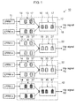
- FIG. 1 is a block diagram of a first embodiment of a power range monitoring system according to the present invention
- FIG. 2 is a top plan view of a printed circuit board equipped with a circuit description element manufactured by a first provider of the first embodiment of the power range monitoring system according to the present invention
- FIG. 3 is a top plan view of the printed circuit board equipped with a circuit description element manufactured by a second provider of the first embodiment of the power range monitoring system according to the present invention
- FIG. 4 is a block diagram of a FPGA Input/Output pattern comparing device of the first embodiment of the power range monitoring system according to the present invention.
- FIG. 5 is a block diagram in a second embodiment of the power range monitoring system according to the present invention.
- FIG. 1 is a block diagram of a first embodiment of a power range monitoring system according to the present invention.
- a power range monitoring system 10 has LPRM (local power range monitor) detectors 11 . It also has APRM (average power range monitor system) units 12 , 22 , 32 , 42 configured to perform a trip judgment based on the signal outputted from the LPRM detector 11 .
- the number of LPRM detectors 11 is “m”, for example.
- the number of APRM units 12 , 22 , 32 , 42 is four, for example.
- APRM units 12 , 22 , 32 , 42 are designed so as to satisfy requirements as outputting a given output signal in response to a given input signal.
- APRM units 12 , 22 , 32 , 42 of this embodiment perform an averaging operation of the signals outputted from m LPRM detectors 11 .
- the trip judgment of APRM units 12 , 22 , 32 , 42 is carried out by judging whether the acquired average value exceeds a given threshold or not. If the trip judgment becomes “TRUE”, each APRM unit 12 , 22 , 32 , 42 outputs a trip signal 18 independently.
- the trip signals 18 which four APRM units 12 , 22 , 32 , 42 output are called trip signal A 1 , trip signal B 1 , trip signal A 2 , and trip signal B 2 , respectively.
- a reactor protection system of a nuclear power plant scrums the nuclear reactor, if trip signal A 1 or A 2 is “TRUE” and trip signal B 1 or B 2 is “TRUE”. Therefore, the design is multiplexed so that a nuclear reactor might not result in scrum with an incorrect trip signal, even if one of the APRM units 12 , 22 , 32 , 42 falls into out of order.
- the reactor protection system may be configured to scrum the nuclear reactor if two or more out of four trip signals become “TRUE”.
- these APRM units 12 , 22 , 32 , 42 are diversity channels.
- Each of the APRM units 12 , 22 , 32 , 42 has LPRM modules 13 , 23 , 33 , 43 . And each of the APRM units 12 , 22 , 32 , 42 has an APRM module 15 , 25 , 35 or 45 , for example.
- Each of the LPRM modules 13 , 23 , 33 , 43 is provided with plurality of printed circuit boards 14 .
- the LPRM module 13 , 23 , 33 or 43 is provided with circuit description elements 17 , 27 , 37 or 47 , respectively, installed on the respective printed circuit board 14 .
- Each of the APRM modules 15 , 25 , 35 , 45 is provided with a printed circuit board 16 .
- the APRM module 15 , 25 , 35 or 45 is provided with circuit description elements 17 , 27 , 37 or 47 , respectively, installed on the respective printed circuit board 16 . That is, each of the APRM units 12 , 22 , 32 , 42 is provided with the printed circuit boards 14 , 16 having a circuit pattern thereon, respectively, and the circuit description elements 17 , 27 , 37 or 47 installed on the printed circuit boards 14 , 16 .
- the circuit description elements 17 , 27 , 37 , 47 are implemented electric circuits described in the hardware description language by a configuration tool. They may be FPGA elements, for example.
- the APRM units 12 , 22 , 32 , 42 are different from each other in the circuit description elements 17 , 27 , 37 , 47 .
- the different circuit description elements 17 , 27 , 37 , 47 are FPGAs manufactured by the different provider (manufacturer).
- the FPGAs may be implemented a single VHDL (VHSIC Hardware Description Language) design by an FPGA configuration tool.
- the single VHDL design is described in the hardware description language so that an implemented FPGA element is configured to have an electric circuit that satisfies the requirements.
- circuit description elements 17 , 27 , 37 , 47 manufactured by the different providers may be different from each other in a pin arrangement of the circuit description elements 17 , 27 , 37 , 47 . Therefore, this embodiment enables it to install these circuit description elements 17 , 27 , 37 , 47 on same printed circuit boards 14 , 16 .
- FIG. 2 is a top plan view of the printed circuit board equipped with a circuit description element manufactured by a first provider of the first embodiment of the power range monitoring system according to the present invention.
- FIG. 3 is a top plan view of the printed circuit board equipped with a circuit description element manufactured by a second provider of the first embodiment of the power range monitoring system according to the present invention.
- FIG. 2 and FIG. 3 indicate the printed circuit board 14 of the LPRM modules 13 , 23 , 33 , 43 , for example, the printed circuit boards 16 of the APRM modules 15 , 25 , 35 , 45 are similar.
- the circuit description element 17 manufactured by the first provider may have a different arrangement of fixed pins, such as a power supply (common pin 51 and ground pin 52 ) of circuit description elements 17 , 27 from the circuit description element 27 manufactured by the second provider. Therefore, in order to use printed circuit boards 14 having a circuit pattern common to the four LPRM modules 13 , 23 , 33 , 43 , all the locations corresponding to the fixed pins in the circuit pattern of the circuit description elements 17 , 27 are configured to be the locations where the fixed pins can be arranged.
- both of the location of the circuit pattern corresponding to the common pin 51 of one circuit description element 17 and the location of the circuit pattern corresponding to the common pin 51 of the other circuit description element 27 are configured to be a wiring 53 for the common pin 51 .
- both of the location of the circuit pattern corresponding to the ground pin 52 of one circuit description element 17 and the location of the circuit pattern corresponding to the ground pin 52 of the other circuit description element 27 are configured to be a wiring 53 for the ground pin 52 .
- the wiring for the common pin 51 and the wiring for the ground pin 52 are provided so that these wirings correspond to two pin positions respectively in the circuit pattern.
- the electric circuit implemented in the circuit description elements 17 , 27 should not be a configuration that a pin 55 of the circuit description elements 17 , 27 corresponding to the fixed pin of the other circuit description element 27 , 17 is assigned to logic. For example, it is described in a hardware description language so that these pins 55 are not assigned as input pins.
- circuit description elements 17 , 27 By using such printed circuit boards 14 and circuit description elements 17 , 27 , even if the circuit description elements 17 , 27 are manufactured by different providers, they can be installed on the printed circuit boards 14 having a same circuit pattern thereon. Also, more than one circuit patterns corresponding to the circuit description elements 17 , 27 manufactured by different providers may be formed at different positions on the printed circuit boards 14 , so that they can be installed on the printed circuit boards 14 having same circuit patterns thereon even if the circuit description elements 17 , 27 are manufactured by different providers.
- the power range monitoring system 10 of this embodiment uses the circuit description elements 17 , 27 , 37 , 47 manufactured by different providers for each diversity APRM unit 12 , 22 , 32 , 42 . Therefore, even if there is a cause of failure common to the circuit description elements manufactured by a certain provider, the cause of failure does not result in a malfunction of the power range monitoring system 10 .
- mutually different circuit description elements 17 , 27 , 37 , 47 can be FPGA elements manufactured by a single provider and implemented mutually different VHDL designs by a single FPGA configuration tool described by different designers so that the electric circuit satisfies requirements. In this case, even if there is an error in a certain VHDL design, the error in the VHDL design does not result in a malfunction of the power range monitoring system 10 .
- mutually different circuit description elements 17 , 27 , 37 , 47 can be FPGA elements manufactured by a single provider and implemented a single VHDL design described in the hardware description language that constitutes the electric circuit that satisfies the requirements by mutually different FPGA configuration tools. In this case, even if there is an error in a certain FPGA configuration tool, the error in a FPGA configuration tool does not result in a malfunction of power range monitoring system 10 .
- circuit description elements 17 , 27 , 37 , 47 constitute the electric circuit that satisfies the requirements or not, for example, by an FPGA Input/Output pattern comparing device.
- FIG. 4 is a block diagram of the FPGA Input/Output pattern comparing device of the first embodiment of the power range monitoring system according to the present invention.
- the FPGA Input/Output pattern comparing device 60 is provided with a simulated input signal generator 61 and an output signal comparator 62 .
- the simulated input signal generator 61 outputs a simulated input signal 63 to target circuit description elements 17 , 27 , 37 , 47 for validation.
- the simulated input signal 63 simulates the input signal to be processed by the target circuit description elements 17 , 27 , 37 , 47 .
- Output signals 64 outputted from the circuit description elements 17 , 27 , 37 , 47 are inputted into the output signal comparator 62 .
- This FPGA Input/Output pattern comparing device 60 compares the voltage values of the output signals and the timings of their changes in response to the same input signals into a plurality of circuit description elements 17 , 27 , 37 , 47 . By this comparison, it can be judged whether the mutually different circuit description elements 17 , 27 , 37 , 47 output the same output signals in response to the same input signals, and then those circuit description elements 17 , 27 , 37 , 47 can be validated. Therefore, it can be judged whether a certain provider, a certain VHDL design, or a certain FPGA configuration tool has an error or not.
- the output signal comparator 62 is, for example, connected to the electric output of the circuit description elements 17 , 27 , 37 , 47 via resistors of the same resistance, and measures the voltage at the connect point.
- the circuit description elements 17 , 27 , 37 , 47 are four FPGA elements of which the output voltage is 0V or 5V for example, if all of the FPGA elements behave in the same manner, the voltage of the connect point must be 0V or 5V. However, if any of the FPGA elements behave differently from other FPGA element, the voltage of the connect point would be a value other than 0V or 5V. So it can be checked whether any of the FPGA has an error by comparing the voltage with thresholds.
- the output signal comparator 62 may have a majority decision processing function.
- the majority decision processing function is to compare the output signals of the FPGA elements in response to a single input signal, and to judge that FPGA elements outputting a majority signal are sound, and the other FPGA elements have a defect. Thus, t a plurality of the circuit description elements 17 , 27 , 37 , 47 can be validated efficiently.
- the FPGA Input/Output pattern comparing device 60 validates circuit description elements 17 , 27 , 37 , 47 by comparing the output signals of circuit description elements 17 , 27 , 37 , 47
- the validation can be performed by comparing the output signals 64 from the LPRM modules 13 , 23 , 33 , 43 , the APRM modules 15 , 25 , 35 , 45 or the whole APRM units 12 , 22 , 32 , 42 , in response to the simulated input signal 63 . In this way, each module as a whole or each unit as a whole can also be validated.
- FIG. 5 is a block diagram in a second embodiment of the power range monitoring system according to the present invention.
- the power range monitoring system 20 of this embodiment is provided with mutually different printed circuit boards 14 , 24 , 34 , 44 for each of the LPRM modules 13 , 23 , 33 , 43 .
- the circuit patterns of these printed circuit boards 14 , 24 , 34 , 44 may be designed by different designers independently so as to satisfy the same requirements.
- mutually different printed circuit boards 16 , 26 , 36 , 46 are also used for each of the APRM units 15 , 25 , 35 , 45 .
- the circuit patterns of these printed circuit boards 16 , 26 , 36 , 46 may be designed by different designers independently so as to satisfy the same requirements.
- All of the APRM units 12 , 22 , 32 , 42 may be provided with the circuit description elements 17 that are the FPGA elements manufactured by a single provider and are implemented the same VHDL design by the single FPGA configuration tool, for example.
- the power range monitoring system 20 of this embodiment is provided with the diversity APRM units 12 , 22 , 32 , 42 different in the circuit patterns formed on the printed circuit boards 14 , 24 , 34 , 44 , 16 , 26 , 36 , 46 . Therefore, even if there is an error in a certain circuit pattern, the error does not result in malfunction of the power range monitoring system 20 .
Landscapes
- Engineering & Computer Science (AREA)
- Theoretical Computer Science (AREA)
- Quality & Reliability (AREA)
- Physics & Mathematics (AREA)
- General Engineering & Computer Science (AREA)
- General Physics & Mathematics (AREA)
- Hardware Redundancy (AREA)
- Monitoring And Testing Of Nuclear Reactors (AREA)
Abstract
Description
Claims (11)
Applications Claiming Priority (2)
| Application Number | Priority Date | Filing Date | Title |
|---|---|---|---|
| JP2007-116403 | 2007-04-26 | ||
| JP2007116403A JP5057837B2 (en) | 2007-04-26 | 2007-04-26 | Redundant system and method for manufacturing redundant system |
Publications (2)
| Publication Number | Publication Date |
|---|---|
| US20090315614A1 US20090315614A1 (en) | 2009-12-24 |
| US8044703B2 true US8044703B2 (en) | 2011-10-25 |
Family
ID=40053490
Family Applications (1)
| Application Number | Title | Priority Date | Filing Date |
|---|---|---|---|
| US12/109,091 Active 2031-03-12 US8044703B2 (en) | 2007-04-26 | 2008-04-24 | Diversity signal processing system and a producing method thereof |
Country Status (2)
| Country | Link |
|---|---|
| US (1) | US8044703B2 (en) |
| JP (1) | JP5057837B2 (en) |
Families Citing this family (6)
| Publication number | Priority date | Publication date | Assignee | Title |
|---|---|---|---|---|
| JP2010249559A (en) * | 2009-04-13 | 2010-11-04 | Toshiba Corp | Digital safety protection system |
| JP5502509B2 (en) * | 2010-01-28 | 2014-05-28 | 株式会社東芝 | Core thermal limit value monitoring apparatus, core monitoring system, and core thermal limit value monitoring method |
| CN106528401B (en) * | 2016-09-28 | 2019-10-11 | 北京广利核系统工程有限公司 | The tripping test method and device of control system based on redundancy structure |
| CN108228403A (en) * | 2016-12-14 | 2018-06-29 | 中国航空工业集团公司西安航空计算技术研究所 | The redundancy management circuit and management method of a kind of redundant fault-tolerant computer system |
| CN110366760B (en) | 2016-12-30 | 2024-05-07 | 纽斯高动力有限责任公司 | Nuclear reactor protection system and method |
| CN109215821B (en) * | 2018-08-14 | 2020-08-07 | 中广核核电运营有限公司 | Method and system for comparing main feed water flow redundancy measurement channels of nuclear power station evaporator |
Citations (3)
| Publication number | Priority date | Publication date | Assignee | Title |
|---|---|---|---|---|
| US4584165A (en) * | 1983-02-09 | 1986-04-22 | General Electric Company | Redundant reactivity control system |
| US5930317A (en) * | 1996-09-27 | 1999-07-27 | Kabushiki Kaisha Toshiba | Power range monitor system for nuclear reactor |
| JP2005249609A (en) | 2004-03-04 | 2005-09-15 | Toshiba Corp | Safety protection instrumentation system and its handling method |
Family Cites Families (7)
| Publication number | Priority date | Publication date | Assignee | Title |
|---|---|---|---|---|
| JPH01142809A (en) * | 1987-11-30 | 1989-06-05 | Toshiba Corp | Diagnostic device for digital input circuit |
| JPH01202624A (en) * | 1988-02-09 | 1989-08-15 | Mitsubishi Electric Corp | Failure determination method for measurement control equipment |
| KR100408493B1 (en) * | 2001-05-07 | 2003-12-06 | 한국전력기술 주식회사 | System for digital reactor protecting to prevent common mode failures and control method of the same |
| JP2003287587A (en) * | 2002-03-27 | 2003-10-10 | Toshiba Corp | Plant protection instrumentation equipment |
| JP2004318254A (en) * | 2003-04-11 | 2004-11-11 | Toshiba Corp | Testing equipment for safety protection measurement equipment |
| JP4568143B2 (en) * | 2005-02-28 | 2010-10-27 | 株式会社東芝 | Safety system verification method and safety system verified by the verification method |
| JP5193416B2 (en) * | 2005-08-24 | 2013-05-08 | 株式会社東芝 | Radiation measurement equipment |
-
2007
- 2007-04-26 JP JP2007116403A patent/JP5057837B2/en not_active Expired - Fee Related
-
2008
- 2008-04-24 US US12/109,091 patent/US8044703B2/en active Active
Patent Citations (4)
| Publication number | Priority date | Publication date | Assignee | Title |
|---|---|---|---|---|
| US4584165A (en) * | 1983-02-09 | 1986-04-22 | General Electric Company | Redundant reactivity control system |
| US5930317A (en) * | 1996-09-27 | 1999-07-27 | Kabushiki Kaisha Toshiba | Power range monitor system for nuclear reactor |
| JP2005249609A (en) | 2004-03-04 | 2005-09-15 | Toshiba Corp | Safety protection instrumentation system and its handling method |
| EP1727157A1 (en) | 2004-03-04 | 2006-11-29 | Kabushiki Kaisha Toshiba | Safety protective instrumentation system and its handling method |
Also Published As
| Publication number | Publication date |
|---|---|
| US20090315614A1 (en) | 2009-12-24 |
| JP5057837B2 (en) | 2012-10-24 |
| JP2008275354A (en) | 2008-11-13 |
Similar Documents
| Publication | Publication Date | Title |
|---|---|---|
| US8044703B2 (en) | Diversity signal processing system and a producing method thereof | |
| JP4801180B2 (en) | Multichannel analog input / output circuit failure diagnosis apparatus and failure diagnosis method | |
| US8117512B2 (en) | Failure detection and mitigation in logic circuits | |
| KR101723932B1 (en) | An method for diagnosing a failure of flight control computer having dual channel | |
| KR101143123B1 (en) | Method and device for determining a probability of occurrence | |
| US7606672B2 (en) | Plant protective instrumentation equipment | |
| US20090164955A1 (en) | Method for verifying safety apparatus and safety apparatus verified by the same | |
| US7774187B2 (en) | Safety protection instrumentation system and method of operating the system | |
| EP2381266B1 (en) | Self-diagnosis system and test circuit determination method | |
| KR100848881B1 (en) | Digital reactor protection system | |
| EP2533154B1 (en) | Failure detection and mitigation in logic circuits | |
| WO2019201597A1 (en) | Wind turbine fault monitoring system and method | |
| CN112987680A (en) | Apparatus, system and method for avoiding fault propagation in a security system | |
| CN110837233B (en) | A safety control system that improves functional safety | |
| US8965735B2 (en) | Signal processing device | |
| CN102591322A (en) | Checking of functions of a control system having components | |
| Abdelawwad et al. | FPGA implementation of a safety system-on-chip based on 1oo4 architecture using LEON3 processor | |
| Battle et al. | Reactor protection system design using application specific integrated circuits | |
| JP3169930B2 (en) | Automatic test pattern generation device and automatic test pattern generation method | |
| JP2004318254A (en) | Testing equipment for safety protection measurement equipment | |
| JP4817646B2 (en) | Custom IC verification apparatus and verification method | |
| US20090307551A1 (en) | Mixed Signal Circuit for an Electronic Protected Control or Regulation System | |
| WO2017058013A1 (en) | A reconfigurable hardware device for providing a reliable output signal as well as a method for providing said reliable output | |
| Lojda et al. | Accelerating Tests of Arithmetic Circuits Through On-FPGA Stimuli Generation and Their Reduction | |
| US20100313091A1 (en) | Apparatus and method for testing semiconductor integrated circuit |
Legal Events
| Date | Code | Title | Description |
|---|---|---|---|
| AS | Assignment |
Owner name: KABUSHIKI KAISHA TOSHIBA, JAPAN Free format text: ASSIGNMENT OF ASSIGNORS INTEREST;ASSIGNORS:KENJYO, HIROAKI;MIYAZAKI, TADASHI;GOTO, YASUSHI;AND OTHERS;REEL/FRAME:020855/0232;SIGNING DATES FROM 20080408 TO 20080418 Owner name: KABUSHIKI KAISHA TOSHIBA, JAPAN Free format text: ASSIGNMENT OF ASSIGNORS INTEREST;ASSIGNORS:KENJYO, HIROAKI;MIYAZAKI, TADASHI;GOTO, YASUSHI;AND OTHERS;SIGNING DATES FROM 20080408 TO 20080418;REEL/FRAME:020855/0232 |
|
| STCF | Information on status: patent grant |
Free format text: PATENTED CASE |
|
| FEPP | Fee payment procedure |
Free format text: PAYOR NUMBER ASSIGNED (ORIGINAL EVENT CODE: ASPN); ENTITY STATUS OF PATENT OWNER: LARGE ENTITY |
|
| FPAY | Fee payment |
Year of fee payment: 4 |
|
| MAFP | Maintenance fee payment |
Free format text: PAYMENT OF MAINTENANCE FEE, 8TH YEAR, LARGE ENTITY (ORIGINAL EVENT CODE: M1552); ENTITY STATUS OF PATENT OWNER: LARGE ENTITY Year of fee payment: 8 |
|
| MAFP | Maintenance fee payment |
Free format text: PAYMENT OF MAINTENANCE FEE, 12TH YEAR, LARGE ENTITY (ORIGINAL EVENT CODE: M1553); ENTITY STATUS OF PATENT OWNER: LARGE ENTITY Year of fee payment: 12 |