US8044390B2 - Material for organic electroluminescent device, organic electroluminescent device, and organic electroluminescent display - Google Patents
Material for organic electroluminescent device, organic electroluminescent device, and organic electroluminescent display Download PDFInfo
- Publication number
- US8044390B2 US8044390B2 US12/601,808 US60180807A US8044390B2 US 8044390 B2 US8044390 B2 US 8044390B2 US 60180807 A US60180807 A US 60180807A US 8044390 B2 US8044390 B2 US 8044390B2
- Authority
- US
- United States
- Prior art keywords
- group
- layer
- organic
- organic electroluminescent
- anode
- Prior art date
- Legal status (The legal status is an assumption and is not a legal conclusion. Google has not performed a legal analysis and makes no representation as to the accuracy of the status listed.)
- Active, expires
Links
- 239000000463 material Substances 0.000 title claims abstract description 92
- 125000004432 carbon atom Chemical group C* 0.000 claims abstract description 73
- 125000003118 aryl group Chemical group 0.000 claims abstract description 51
- 125000000217 alkyl group Chemical group 0.000 claims abstract description 39
- 125000004435 hydrogen atom Chemical class [H]* 0.000 claims abstract description 31
- 125000004093 cyano group Chemical group *C#N 0.000 claims abstract description 29
- 125000000623 heterocyclic group Chemical group 0.000 claims abstract description 29
- 125000003709 fluoroalkyl group Chemical group 0.000 claims abstract description 24
- 125000005843 halogen group Chemical group 0.000 claims abstract description 20
- 229910052757 nitrogen Inorganic materials 0.000 claims abstract description 19
- 239000001257 hydrogen Substances 0.000 claims abstract description 17
- 229910052739 hydrogen Inorganic materials 0.000 claims abstract description 17
- 150000002466 imines Chemical class 0.000 claims abstract description 16
- 229910052799 carbon Inorganic materials 0.000 claims abstract description 8
- 125000004433 nitrogen atom Chemical group N* 0.000 claims abstract description 8
- 239000010410 layer Substances 0.000 claims description 265
- -1 phenylenediamine compound Chemical class 0.000 claims description 74
- 239000000758 substrate Substances 0.000 claims description 34
- 239000012044 organic layer Substances 0.000 claims description 27
- 229910052751 metal Inorganic materials 0.000 claims description 26
- 239000002184 metal Substances 0.000 claims description 26
- 229910052782 aluminium Inorganic materials 0.000 claims description 22
- XAGFODPZIPBFFR-UHFFFAOYSA-N aluminium Chemical compound [Al] XAGFODPZIPBFFR-UHFFFAOYSA-N 0.000 claims description 22
- 229910052731 fluorine Inorganic materials 0.000 claims description 20
- 239000011737 fluorine Substances 0.000 claims description 19
- 229910000838 Al alloy Inorganic materials 0.000 claims description 17
- WEVYAHXRMPXWCK-UHFFFAOYSA-N Acetonitrile Chemical compound CC#N WEVYAHXRMPXWCK-UHFFFAOYSA-N 0.000 claims description 15
- 230000009467 reduction Effects 0.000 claims description 14
- 125000003983 fluorenyl group Chemical group C1(=CC=CC=2C3=CC=CC=C3CC12)* 0.000 claims description 13
- 125000001997 phenyl group Chemical group [H]C1=C([H])C([H])=C(*)C([H])=C1[H] 0.000 claims description 12
- PXGOKWXKJXAPGV-UHFFFAOYSA-N Fluorine Chemical compound FF PXGOKWXKJXAPGV-UHFFFAOYSA-N 0.000 claims description 11
- 125000001153 fluoro group Chemical group F* 0.000 claims description 9
- 125000001624 naphthyl group Chemical group 0.000 claims description 9
- 125000000609 carbazolyl group Chemical group C1(=CC=CC=2C3=CC=CC=C3NC12)* 0.000 claims description 8
- 150000004767 nitrides Chemical class 0.000 claims description 8
- 125000002023 trifluoromethyl group Chemical group FC(F)(F)* 0.000 claims description 7
- 229910044991 metal oxide Inorganic materials 0.000 claims description 5
- 150000004706 metal oxides Chemical class 0.000 claims description 5
- KTWOOEGAPBSYNW-UHFFFAOYSA-N ferrocene Chemical compound [Fe+2].C=1C=C[CH-]C=1.C=1C=C[CH-]C=1 KTWOOEGAPBSYNW-UHFFFAOYSA-N 0.000 claims description 4
- 150000001875 compounds Chemical class 0.000 description 144
- 239000010408 film Substances 0.000 description 43
- 230000015572 biosynthetic process Effects 0.000 description 25
- 230000006870 function Effects 0.000 description 24
- 238000003786 synthesis reaction Methods 0.000 description 22
- YMWUJEATGCHHMB-UHFFFAOYSA-N Dichloromethane Chemical compound ClCCl YMWUJEATGCHHMB-UHFFFAOYSA-N 0.000 description 21
- 0 [1*]C1=CC2=C(C=C1[2*])/C(=N/[N+]#[C-])C1=CC([3*])=C([4*])C=C1/C2=N/C#N.[1*]C1=CC2=C(C=C1[2*])/C(=N\C#N)C1=CC([3*])=C([4*])C=C1/C2=N/C#N Chemical compound [1*]C1=CC2=C(C=C1[2*])/C(=N/[N+]#[C-])C1=CC([3*])=C([4*])C=C1/C2=N/C#N.[1*]C1=CC2=C(C=C1[2*])/C(=N\C#N)C1=CC([3*])=C([4*])C=C1/C2=N/C#N 0.000 description 19
- 238000000034 method Methods 0.000 description 19
- 125000001424 substituent group Chemical group 0.000 description 19
- 239000000243 solution Substances 0.000 description 18
- 239000000203 mixture Substances 0.000 description 17
- 238000000151 deposition Methods 0.000 description 16
- 238000000859 sublimation Methods 0.000 description 16
- 230000008022 sublimation Effects 0.000 description 16
- 238000010521 absorption reaction Methods 0.000 description 15
- 125000003545 alkoxy group Chemical group 0.000 description 15
- 239000002019 doping agent Substances 0.000 description 15
- 230000008021 deposition Effects 0.000 description 14
- 229910052783 alkali metal Inorganic materials 0.000 description 13
- 150000001340 alkali metals Chemical class 0.000 description 13
- QTBSBXVTEAMEQO-UHFFFAOYSA-N Acetic acid Chemical compound CC(O)=O QTBSBXVTEAMEQO-UHFFFAOYSA-N 0.000 description 12
- 238000005259 measurement Methods 0.000 description 12
- 239000010409 thin film Substances 0.000 description 12
- 239000007924 injection Substances 0.000 description 11
- 238000002347 injection Methods 0.000 description 11
- 238000004949 mass spectrometry Methods 0.000 description 11
- BBEAQIROQSPTKN-UHFFFAOYSA-N pyrene Chemical compound C1=CC=C2C=CC3=CC=CC4=CC=C1C2=C43 BBEAQIROQSPTKN-UHFFFAOYSA-N 0.000 description 11
- 239000007787 solid Substances 0.000 description 11
- 238000001771 vacuum deposition Methods 0.000 description 11
- JUJWROOIHBZHMG-UHFFFAOYSA-N Pyridine Chemical group C1=CC=NC=C1 JUJWROOIHBZHMG-UHFFFAOYSA-N 0.000 description 10
- 125000004104 aryloxy group Chemical group 0.000 description 10
- 125000000753 cycloalkyl group Chemical group 0.000 description 10
- 239000003446 ligand Substances 0.000 description 10
- 125000002496 methyl group Chemical group [H]C([H])([H])* 0.000 description 10
- 229910052784 alkaline earth metal Inorganic materials 0.000 description 9
- 150000001342 alkaline earth metals Chemical class 0.000 description 9
- 125000002915 carbonyl group Chemical group [*:2]C([*:1])=O 0.000 description 9
- SYGWYBOJXOGMRU-UHFFFAOYSA-N chembl233051 Chemical compound C1=CC=C2C3=CC(C(N(CCN(C)C)C4=O)=O)=C5C4=CC=CC5=C3SC2=C1 SYGWYBOJXOGMRU-UHFFFAOYSA-N 0.000 description 9
- 230000000052 comparative effect Effects 0.000 description 9
- 125000006413 ring segment Chemical group 0.000 description 9
- 238000007740 vapor deposition Methods 0.000 description 9
- 229910045601 alloy Inorganic materials 0.000 description 8
- 239000000956 alloy Substances 0.000 description 8
- MWPLVEDNUUSJAV-UHFFFAOYSA-N anthracene Chemical compound C1=CC=CC2=CC3=CC=CC=C3C=C21 MWPLVEDNUUSJAV-UHFFFAOYSA-N 0.000 description 8
- 150000004696 coordination complex Chemical group 0.000 description 8
- 238000004519 manufacturing process Methods 0.000 description 8
- 230000001603 reducing effect Effects 0.000 description 8
- VYPSYNLAJGMNEJ-UHFFFAOYSA-N silicon dioxide Inorganic materials O=[Si]=O VYPSYNLAJGMNEJ-UHFFFAOYSA-N 0.000 description 8
- 238000004528 spin coating Methods 0.000 description 8
- 239000000126 substance Substances 0.000 description 8
- VHNBXOGXYBZHLT-CNFMPTLVSA-N CC.CC.CC.CC.CC.CC.CC.CC.N#C/N=C1/C2=NC(C3=CC=CC=C3)=C(C3=CC=CC=C3)N=C2/C(=N/C#N)C2=C1N=C(C1=CC=CC=C1)C(C1=CC=CC=C1)=N2.[C-]#[N+]/N=C1\C2=NC(C3=CC=CC=C3)=C(C3=CC=CC=C3)N=C2/C(=N/C#N)C2=C1N=C(C1=CC=CC=C1)C(C1=CC=CC=C1)=N2 Chemical compound CC.CC.CC.CC.CC.CC.CC.CC.N#C/N=C1/C2=NC(C3=CC=CC=C3)=C(C3=CC=CC=C3)N=C2/C(=N/C#N)C2=C1N=C(C1=CC=CC=C1)C(C1=CC=CC=C1)=N2.[C-]#[N+]/N=C1\C2=NC(C3=CC=CC=C3)=C(C3=CC=CC=C3)N=C2/C(=N/C#N)C2=C1N=C(C1=CC=CC=C1)C(C1=CC=CC=C1)=N2 VHNBXOGXYBZHLT-CNFMPTLVSA-N 0.000 description 7
- YTPLMLYBLZKORZ-UHFFFAOYSA-N Thiophene Chemical group C=1C=CSC=1 YTPLMLYBLZKORZ-UHFFFAOYSA-N 0.000 description 7
- 125000000732 arylene group Chemical group 0.000 description 7
- 230000005684 electric field Effects 0.000 description 7
- 239000011521 glass Substances 0.000 description 7
- 150000004820 halides Chemical class 0.000 description 7
- 125000000449 nitro group Chemical group [O-][N+](*)=O 0.000 description 7
- MCJGNVYPOGVAJF-UHFFFAOYSA-N quinolin-8-ol Chemical class C1=CN=C2C(O)=CC=CC2=C1 MCJGNVYPOGVAJF-UHFFFAOYSA-N 0.000 description 7
- OKKJLVBELUTLKV-UHFFFAOYSA-N Methanol Chemical compound OC OKKJLVBELUTLKV-UHFFFAOYSA-N 0.000 description 6
- 125000003277 amino group Chemical group 0.000 description 6
- 229910052792 caesium Inorganic materials 0.000 description 6
- JCGRMAWAPVVHFK-UHFFFAOYSA-N chrysene-6,12-diamine Chemical compound C1=CC=C2C(N)=CC3=C(C=CC=C4)C4=C(N)C=C3C2=C1 JCGRMAWAPVVHFK-UHFFFAOYSA-N 0.000 description 6
- GVEPBJHOBDJJJI-UHFFFAOYSA-N fluoranthrene Natural products C1=CC(C2=CC=CC=C22)=C3C2=CC=CC3=C1 GVEPBJHOBDJJJI-UHFFFAOYSA-N 0.000 description 6
- 229910052747 lanthanoid Inorganic materials 0.000 description 6
- 150000002602 lanthanoids Chemical class 0.000 description 6
- PQXKHYXIUOZZFA-UHFFFAOYSA-M lithium fluoride Chemical compound [Li+].[F-] PQXKHYXIUOZZFA-UHFFFAOYSA-M 0.000 description 6
- 235000019557 luminance Nutrition 0.000 description 6
- BASFCYQUMIYNBI-UHFFFAOYSA-N platinum Chemical compound [Pt] BASFCYQUMIYNBI-UHFFFAOYSA-N 0.000 description 6
- 239000002244 precipitate Substances 0.000 description 6
- 238000000746 purification Methods 0.000 description 6
- 239000004065 semiconductor Substances 0.000 description 6
- LFQSCWFLJHTTHZ-UHFFFAOYSA-N Ethanol Chemical compound CCO LFQSCWFLJHTTHZ-UHFFFAOYSA-N 0.000 description 5
- 125000003710 aryl alkyl group Chemical group 0.000 description 5
- 238000006243 chemical reaction Methods 0.000 description 5
- 238000001816 cooling Methods 0.000 description 5
- 239000010949 copper Substances 0.000 description 5
- 125000000113 cyclohexyl group Chemical group [H]C1([H])C([H])([H])C([H])([H])C([H])(*)C([H])([H])C1([H])[H] 0.000 description 5
- 125000001072 heteroaryl group Chemical group 0.000 description 5
- 125000002887 hydroxy group Chemical group [H]O* 0.000 description 5
- 150000002739 metals Chemical class 0.000 description 5
- 229960003540 oxyquinoline Drugs 0.000 description 5
- 229920006395 saturated elastomer Polymers 0.000 description 5
- 239000011734 sodium Substances 0.000 description 5
- 239000002904 solvent Substances 0.000 description 5
- 238000004544 sputter deposition Methods 0.000 description 5
- 125000000999 tert-butyl group Chemical group [H]C([H])([H])C(*)(C([H])([H])[H])C([H])([H])[H] 0.000 description 5
- 238000002834 transmittance Methods 0.000 description 5
- XKRFYHLGVUSROY-UHFFFAOYSA-N Argon Chemical group [Ar] XKRFYHLGVUSROY-UHFFFAOYSA-N 0.000 description 4
- KYQCOXFCLRTKLS-UHFFFAOYSA-N Pyrazine Chemical compound C1=CN=CC=N1 KYQCOXFCLRTKLS-UHFFFAOYSA-N 0.000 description 4
- 125000004453 alkoxycarbonyl group Chemical group 0.000 description 4
- 150000001454 anthracenes Chemical class 0.000 description 4
- 150000004982 aromatic amines Chemical class 0.000 description 4
- 125000005110 aryl thio group Chemical group 0.000 description 4
- XJHCXCQVJFPJIK-UHFFFAOYSA-M caesium fluoride Chemical compound [F-].[Cs+] XJHCXCQVJFPJIK-UHFFFAOYSA-M 0.000 description 4
- 238000010586 diagram Methods 0.000 description 4
- 125000001495 ethyl group Chemical group [H]C([H])([H])C([H])([H])* 0.000 description 4
- 230000002093 peripheral effect Effects 0.000 description 4
- 229910052697 platinum Inorganic materials 0.000 description 4
- UMJSCPRVCHMLSP-UHFFFAOYSA-N pyridine Natural products COC1=CC=CN=C1 UMJSCPRVCHMLSP-UHFFFAOYSA-N 0.000 description 4
- 229910052761 rare earth metal Inorganic materials 0.000 description 4
- 150000002910 rare earth metals Chemical class 0.000 description 4
- 229910052708 sodium Inorganic materials 0.000 description 4
- XOLBLPGZBRYERU-UHFFFAOYSA-N tin dioxide Chemical compound O=[Sn]=O XOLBLPGZBRYERU-UHFFFAOYSA-N 0.000 description 4
- XJDNKRIXUMDJCW-UHFFFAOYSA-J titanium tetrachloride Chemical compound Cl[Ti](Cl)(Cl)Cl XJDNKRIXUMDJCW-UHFFFAOYSA-J 0.000 description 4
- SIEYGCOROKCHEO-UHFFFAOYSA-N 6-n,6-n,12-n,12-n-tetrakis(3,4-dimethylphenyl)chrysene-6,12-diamine Chemical compound C1=C(C)C(C)=CC=C1N(C=1C2=CC=CC=C2C2=CC(=C3C=CC=CC3=C2C=1)N(C=1C=C(C)C(C)=CC=1)C=1C=C(C)C(C)=CC=1)C1=CC=C(C)C(C)=C1 SIEYGCOROKCHEO-UHFFFAOYSA-N 0.000 description 3
- 239000005725 8-Hydroxyquinoline Substances 0.000 description 3
- ODINCKMPIJJUCX-UHFFFAOYSA-N Calcium oxide Chemical compound [Ca]=O ODINCKMPIJJUCX-UHFFFAOYSA-N 0.000 description 3
- RYGMFSIKBFXOCR-UHFFFAOYSA-N Copper Chemical compound [Cu] RYGMFSIKBFXOCR-UHFFFAOYSA-N 0.000 description 3
- IAZDPXIOMUYVGZ-UHFFFAOYSA-N Dimethylsulphoxide Chemical compound CS(C)=O IAZDPXIOMUYVGZ-UHFFFAOYSA-N 0.000 description 3
- KFZMGEQAYNKOFK-UHFFFAOYSA-N Isopropanol Chemical compound CC(C)O KFZMGEQAYNKOFK-UHFFFAOYSA-N 0.000 description 3
- PXHVJJICTQNCMI-UHFFFAOYSA-N Nickel Chemical compound [Ni] PXHVJJICTQNCMI-UHFFFAOYSA-N 0.000 description 3
- 239000007983 Tris buffer Substances 0.000 description 3
- 125000006615 aromatic heterocyclic group Chemical group 0.000 description 3
- 125000001769 aryl amino group Chemical group 0.000 description 3
- 229910052788 barium Inorganic materials 0.000 description 3
- 230000008901 benefit Effects 0.000 description 3
- 125000006267 biphenyl group Chemical group 0.000 description 3
- 125000003917 carbamoyl group Chemical group [H]N([H])C(*)=O 0.000 description 3
- 125000003178 carboxy group Chemical group [H]OC(*)=O 0.000 description 3
- 239000013522 chelant Substances 0.000 description 3
- 229910052801 chlorine Inorganic materials 0.000 description 3
- 239000011651 chromium Substances 0.000 description 3
- 238000000576 coating method Methods 0.000 description 3
- 239000000470 constituent Substances 0.000 description 3
- 229910052802 copper Inorganic materials 0.000 description 3
- 125000001511 cyclopentyl group Chemical group [H]C1([H])C([H])([H])C([H])([H])C([H])(*)C1([H])[H] 0.000 description 3
- 230000007547 defect Effects 0.000 description 3
- 125000005567 fluorenylene group Chemical group 0.000 description 3
- 150000002222 fluorine compounds Chemical class 0.000 description 3
- 239000010931 gold Substances 0.000 description 3
- 125000005549 heteroarylene group Chemical group 0.000 description 3
- 150000002430 hydrocarbons Chemical group 0.000 description 3
- RAXXELZNTBOGNW-UHFFFAOYSA-N imidazole Natural products C1=CNC=N1 RAXXELZNTBOGNW-UHFFFAOYSA-N 0.000 description 3
- 150000002484 inorganic compounds Chemical class 0.000 description 3
- 229910010272 inorganic material Inorganic materials 0.000 description 3
- 125000001449 isopropyl group Chemical group [H]C([H])([H])C([H])(*)C([H])([H])[H] 0.000 description 3
- 239000011777 magnesium Substances 0.000 description 3
- KSVMTHKYDGMXFJ-UHFFFAOYSA-N n,n'-bis(trimethylsilyl)methanediimine Chemical compound C[Si](C)(C)N=C=N[Si](C)(C)C KSVMTHKYDGMXFJ-UHFFFAOYSA-N 0.000 description 3
- 150000004866 oxadiazoles Chemical class 0.000 description 3
- 229910052700 potassium Inorganic materials 0.000 description 3
- 239000010453 quartz Substances 0.000 description 3
- 238000005215 recombination Methods 0.000 description 3
- 230000006798 recombination Effects 0.000 description 3
- 239000011347 resin Substances 0.000 description 3
- 229920005989 resin Polymers 0.000 description 3
- 229910052701 rubidium Inorganic materials 0.000 description 3
- 229930195734 saturated hydrocarbon Natural products 0.000 description 3
- 125000002914 sec-butyl group Chemical group [H]C([H])([H])C([H])([H])C([H])(*)C([H])([H])[H] 0.000 description 3
- 229910052710 silicon Inorganic materials 0.000 description 3
- 125000003808 silyl group Chemical group [H][Si]([H])([H])[*] 0.000 description 3
- PJANXHGTPQOBST-UHFFFAOYSA-N stilbene Chemical group C=1C=CC=CC=1C=CC1=CC=CC=C1 PJANXHGTPQOBST-UHFFFAOYSA-N 0.000 description 3
- 238000003756 stirring Methods 0.000 description 3
- 229930192474 thiophene Natural products 0.000 description 3
- 230000032258 transport Effects 0.000 description 3
- 229930195735 unsaturated hydrocarbon Natural products 0.000 description 3
- UWRZIZXBOLBCON-VOTSOKGWSA-N (e)-2-phenylethenamine Chemical class N\C=C\C1=CC=CC=C1 UWRZIZXBOLBCON-VOTSOKGWSA-N 0.000 description 2
- VERMWGQSKPXSPZ-BUHFOSPRSA-N 1-[(e)-2-phenylethenyl]anthracene Chemical class C=1C=CC2=CC3=CC=CC=C3C=C2C=1\C=C\C1=CC=CC=C1 VERMWGQSKPXSPZ-BUHFOSPRSA-N 0.000 description 2
- SHMZQZUAVVRSFL-UHFFFAOYSA-N 1-n,1-n,4-n,4-n-tetrakis(4-methylphenyl)naphthalene-1,4-diamine Chemical compound C1=CC(C)=CC=C1N(C=1C2=CC=CC=C2C(N(C=2C=CC(C)=CC=2)C=2C=CC(C)=CC=2)=CC=1)C1=CC=C(C)C=C1 SHMZQZUAVVRSFL-UHFFFAOYSA-N 0.000 description 2
- PYEHNRLHKXCVRI-UHFFFAOYSA-N 1-n,1-n-diethyl-4-n-phenyl-4-n-pyren-1-ylbenzene-1,4-diamine Chemical compound C1=CC(N(CC)CC)=CC=C1N(C=1C2=CC=C3C=CC=C4C=CC(C2=C43)=CC=1)C1=CC=CC=C1 PYEHNRLHKXCVRI-UHFFFAOYSA-N 0.000 description 2
- MHDPSZLABGCAQF-UHFFFAOYSA-N 10-[10-(4-methyl-n-(4-methylphenyl)anilino)anthracen-9-yl]-n,n-bis(4-methylphenyl)anthracen-9-amine Chemical compound C1=CC(C)=CC=C1N(C=1C2=CC=CC=C2C(C=2C3=CC=CC=C3C(N(C=3C=CC(C)=CC=3)C=3C=CC(C)=CC=3)=C3C=CC=CC3=2)=C2C=CC=CC2=1)C1=CC=C(C)C=C1 MHDPSZLABGCAQF-UHFFFAOYSA-N 0.000 description 2
- IXHWGNYCZPISET-UHFFFAOYSA-N 2-[4-(dicyanomethylidene)-2,3,5,6-tetrafluorocyclohexa-2,5-dien-1-ylidene]propanedinitrile Chemical compound FC1=C(F)C(=C(C#N)C#N)C(F)=C(F)C1=C(C#N)C#N IXHWGNYCZPISET-UHFFFAOYSA-N 0.000 description 2
- FVZDAUFUGNBRPX-UHFFFAOYSA-N 2-n,6-n-dinaphthalen-2-yl-2-n,6-n-diphenylnaphthalene-2,6-diamine Chemical compound C1=CC=CC=C1N(C=1C=C2C=CC(=CC2=CC=1)N(C=1C=CC=CC=1)C=1C=C2C=CC=CC2=CC=1)C1=CC=C(C=CC=C2)C2=C1 FVZDAUFUGNBRPX-UHFFFAOYSA-N 0.000 description 2
- FXDUVIGDTNKKFF-UHFFFAOYSA-N 3-n,3-n,9-n,9-n-tetraphenylperylene-3,9-diamine Chemical compound C1=CC=CC=C1N(C=1C=2C=CC=C3C=4C=CC(=C5C=CC=C(C=45)C(C=23)=CC=1)N(C=1C=CC=CC=1)C=1C=CC=CC=1)C1=CC=CC=C1 FXDUVIGDTNKKFF-UHFFFAOYSA-N 0.000 description 2
- 125000001255 4-fluorophenyl group Chemical group [H]C1=C([H])C(*)=C([H])C([H])=C1F 0.000 description 2
- LHZUSBVVRKNNGZ-UHFFFAOYSA-N 6-n,12-n-bis(2,3-dimethylphenyl)-6-n,12-n-bis(3-methyl-5,6,7,8-tetrahydronaphthalen-1-yl)chrysene-6,12-diamine Chemical compound C=1C(C)=CC=2CCCCC=2C=1N(C=1C2=CC=CC=C2C2=CC(=C3C=CC=CC3=C2C=1)N(C=1C(=C(C)C=CC=1)C)C=1C=2CCCCC=2C=C(C)C=1)C1=CC=CC(C)=C1C LHZUSBVVRKNNGZ-UHFFFAOYSA-N 0.000 description 2
- OMRMKWMTMRUYRE-UHFFFAOYSA-N 6-n,12-n-bis(3,4-dimethylphenyl)-6-n,12-n-bis(3,4,5-trimethylphenyl)chrysene-6,12-diamine Chemical compound C1=C(C)C(C)=CC=C1N(C=1C2=CC=CC=C2C2=CC(=C3C=CC=CC3=C2C=1)N(C=1C=C(C)C(C)=CC=1)C=1C=C(C)C(C)=C(C)C=1)C1=CC(C)=C(C)C(C)=C1 OMRMKWMTMRUYRE-UHFFFAOYSA-N 0.000 description 2
- ZKLQGBLMVZGERV-UHFFFAOYSA-N 6-n,12-n-bis(3,4-dimethylphenyl)-6-n,12-n-bis(3,5-dimethyl-4-propan-2-ylphenyl)chrysene-6,12-diamine Chemical compound C1=C(C)C(C(C)C)=C(C)C=C1N(C=1C2=CC=CC=C2C2=CC(=C3C=CC=CC3=C2C=1)N(C=1C=C(C)C(C)=CC=1)C=1C=C(C)C(C(C)C)=C(C)C=1)C1=CC=C(C)C(C)=C1 ZKLQGBLMVZGERV-UHFFFAOYSA-N 0.000 description 2
- LLNVLDSKZWOJHX-UHFFFAOYSA-N 6-n,12-n-bis(3,4-dimethylphenyl)-6-n,12-n-bis(4-methylphenyl)chrysene-6,12-diamine Chemical compound C1=CC(C)=CC=C1N(C=1C2=CC=CC=C2C2=CC(=C3C=CC=CC3=C2C=1)N(C=1C=CC(C)=CC=1)C=1C=C(C)C(C)=CC=1)C1=CC=C(C)C(C)=C1 LLNVLDSKZWOJHX-UHFFFAOYSA-N 0.000 description 2
- XBKTUEWIBUETDF-UHFFFAOYSA-N 6-n,12-n-bis(3,4-dimethylphenyl)-6-n,12-n-dinaphthalen-2-ylchrysene-6,12-diamine Chemical compound C1=C(C)C(C)=CC=C1N(C=1C2=CC=CC=C2C2=CC(=C3C=CC=CC3=C2C=1)N(C=1C=C(C)C(C)=CC=1)C=1C=C2C=CC=CC2=CC=1)C1=CC=C(C=CC=C2)C2=C1 XBKTUEWIBUETDF-UHFFFAOYSA-N 0.000 description 2
- SITPNQQPDJLEMZ-UHFFFAOYSA-N 6-n,12-n-bis(3,5-dimethylphenyl)-6-n,12-n-bis(3,4,5-trimethylphenyl)chrysene-6,12-diamine Chemical compound CC1=CC(C)=CC(N(C=2C=C(C)C(C)=C(C)C=2)C=2C3=CC=CC=C3C3=CC(=C4C=CC=CC4=C3C=2)N(C=2C=C(C)C=C(C)C=2)C=2C=C(C)C(C)=C(C)C=2)=C1 SITPNQQPDJLEMZ-UHFFFAOYSA-N 0.000 description 2
- HUKQTJQEMOJBSR-UHFFFAOYSA-N 6-n,12-n-bis(3,5-dimethylphenyl)-6-n,12-n-bis(3-methyl-5-propan-2-ylphenyl)chrysene-6,12-diamine Chemical compound CC(C)C1=CC(C)=CC(N(C=2C=C(C)C=C(C)C=2)C=2C3=CC=CC=C3C3=CC(=C4C=CC=CC4=C3C=2)N(C=2C=C(C)C=C(C)C=2)C=2C=C(C=C(C)C=2)C(C)C)=C1 HUKQTJQEMOJBSR-UHFFFAOYSA-N 0.000 description 2
- UPNVWUCGGGGZBS-UHFFFAOYSA-N 6-n,12-n-bis(3,5-dimethylphenyl)-6-n,12-n-bis[3-(1,1-diphenylethyl)-5-methylphenyl]chrysene-6,12-diamine Chemical compound CC1=CC(C)=CC(N(C=2C=C(C=C(C)C=2)C(C)(C=2C=CC=CC=2)C=2C=CC=CC=2)C=2C3=CC=CC=C3C3=CC(=C4C=CC=CC4=C3C=2)N(C=2C=C(C)C=C(C)C=2)C=2C=C(C=C(C)C=2)C(C)(C=2C=CC=CC=2)C=2C=CC=CC=2)=C1 UPNVWUCGGGGZBS-UHFFFAOYSA-N 0.000 description 2
- OFGURDJAEJIEPN-UHFFFAOYSA-N 6-n,12-n-bis(3,5-ditert-butylphenyl)-6-n,12-n-bis(3,4,5-trimethylphenyl)chrysene-6,12-diamine Chemical compound CC1=C(C)C(C)=CC(N(C=2C=C(C=C(C=2)C(C)(C)C)C(C)(C)C)C=2C3=CC=CC=C3C3=CC(=C4C=CC=CC4=C3C=2)N(C=2C=C(C)C(C)=C(C)C=2)C=2C=C(C=C(C=2)C(C)(C)C)C(C)(C)C)=C1 OFGURDJAEJIEPN-UHFFFAOYSA-N 0.000 description 2
- CVDVQJRVOXPKTQ-UHFFFAOYSA-N 6-n,12-n-bis(3,5-ditert-butylphenyl)-6-n,12-n-bis(3,4-dimethylphenyl)chrysene-6,12-diamine Chemical compound C1=C(C)C(C)=CC=C1N(C=1C2=CC=CC=C2C2=CC(=C3C=CC=CC3=C2C=1)N(C=1C=C(C)C(C)=CC=1)C=1C=C(C=C(C=1)C(C)(C)C)C(C)(C)C)C1=CC(C(C)(C)C)=CC(C(C)(C)C)=C1 CVDVQJRVOXPKTQ-UHFFFAOYSA-N 0.000 description 2
- ZVDIBHFCWBSPMQ-UHFFFAOYSA-N 6-n,12-n-bis(3,5-ditert-butylphenyl)-6-n,12-n-bis(3,5-dimethylphenyl)chrysene-6,12-diamine Chemical compound CC1=CC(C)=CC(N(C=2C=C(C=C(C=2)C(C)(C)C)C(C)(C)C)C=2C3=CC=CC=C3C3=CC(=C4C=CC=CC4=C3C=2)N(C=2C=C(C)C=C(C)C=2)C=2C=C(C=C(C=2)C(C)(C)C)C(C)(C)C)=C1 ZVDIBHFCWBSPMQ-UHFFFAOYSA-N 0.000 description 2
- VRQVGCPOQBMUBY-UHFFFAOYSA-N 6-n,12-n-bis(3,5-ditert-butylphenyl)-6-n,12-n-bis(3-methyl-5-propan-2-ylphenyl)chrysene-6,12-diamine Chemical compound CC(C)C1=CC(C)=CC(N(C=2C=C(C=C(C=2)C(C)(C)C)C(C)(C)C)C=2C3=CC=CC=C3C3=CC(=C4C=CC=CC4=C3C=2)N(C=2C=C(C=C(C)C=2)C(C)C)C=2C=C(C=C(C=2)C(C)(C)C)C(C)(C)C)=C1 VRQVGCPOQBMUBY-UHFFFAOYSA-N 0.000 description 2
- DEDBWRWOSNFZJH-UHFFFAOYSA-N 6-n,12-n-bis(3,5-ditert-butylphenyl)-6-n,12-n-bis(4-ethyl-3-methylphenyl)chrysene-6,12-diamine Chemical compound C1=C(C)C(CC)=CC=C1N(C=1C2=CC=CC=C2C2=CC(=C3C=CC=CC3=C2C=1)N(C=1C=C(C)C(CC)=CC=1)C=1C=C(C=C(C=1)C(C)(C)C)C(C)(C)C)C1=CC(C(C)(C)C)=CC(C(C)(C)C)=C1 DEDBWRWOSNFZJH-UHFFFAOYSA-N 0.000 description 2
- RQFNSSUNEIBIGU-UHFFFAOYSA-N 6-n,12-n-bis(3,5-ditert-butylphenyl)-6-n,12-n-dinaphthalen-2-ylchrysene-6,12-diamine Chemical compound CC(C)(C)C1=CC(C(C)(C)C)=CC(N(C=2C=C3C=CC=CC3=CC=2)C=2C3=CC=CC=C3C3=CC(=C4C=CC=CC4=C3C=2)N(C=2C=C3C=CC=CC3=CC=2)C=2C=C(C=C(C=2)C(C)(C)C)C(C)(C)C)=C1 RQFNSSUNEIBIGU-UHFFFAOYSA-N 0.000 description 2
- JBSGIWZNUUUNBB-UHFFFAOYSA-N 6-n,12-n-bis(4-ethylphenyl)-6-n,12-n-diphenylchrysene-6,12-diamine Chemical compound C1=CC(CC)=CC=C1N(C=1C2=CC=CC=C2C2=CC(=C3C=CC=CC3=C2C=1)N(C=1C=CC=CC=1)C=1C=CC(CC)=CC=1)C1=CC=CC=C1 JBSGIWZNUUUNBB-UHFFFAOYSA-N 0.000 description 2
- AFDNWCAUHSAJMK-UHFFFAOYSA-N 6-n,12-n-bis(4-methylphenyl)-6-n,12-n-diphenylchrysene-6,12-diamine Chemical compound C1=CC(C)=CC=C1N(C=1C2=CC=CC=C2C2=CC(=C3C=CC=CC3=C2C=1)N(C=1C=CC=CC=1)C=1C=CC(C)=CC=1)C1=CC=CC=C1 AFDNWCAUHSAJMK-UHFFFAOYSA-N 0.000 description 2
- HQGJBNOVSBWSFD-UHFFFAOYSA-N 6-n,12-n-bis(4-tert-butylphenyl)-6-n,12-n-diphenylchrysene-6,12-diamine Chemical compound C1=CC(C(C)(C)C)=CC=C1N(C=1C2=CC=CC=C2C2=CC(=C3C=CC=CC3=C2C=1)N(C=1C=CC=CC=1)C=1C=CC(=CC=1)C(C)(C)C)C1=CC=CC=C1 HQGJBNOVSBWSFD-UHFFFAOYSA-N 0.000 description 2
- DHYTYKVPYXQDFZ-UHFFFAOYSA-N 6-n,12-n-bis(9,9-dimethylfluoren-3-yl)-6-n,12-n-bis(3,4,5-trimethylphenyl)chrysene-6,12-diamine Chemical compound CC1=C(C)C(C)=CC(N(C=2C=C3C(C(C4=CC=CC=C43)(C)C)=CC=2)C=2C3=CC=CC=C3C3=CC(=C4C=CC=CC4=C3C=2)N(C=2C=C3C(C(C4=CC=CC=C43)(C)C)=CC=2)C=2C=C(C)C(C)=C(C)C=2)=C1 DHYTYKVPYXQDFZ-UHFFFAOYSA-N 0.000 description 2
- SURFTGCGCZGRNU-UHFFFAOYSA-N 6-n,12-n-bis(9,9-dimethylfluoren-3-yl)-6-n,12-n-bis(3,4-dimethylphenyl)chrysene-6,12-diamine Chemical compound C1=C(C)C(C)=CC=C1N(C=1C2=CC=CC=C2C2=CC(=C3C=CC=CC3=C2C=1)N(C=1C=C2C(C(C3=CC=CC=C32)(C)C)=CC=1)C=1C=C(C)C(C)=CC=1)C1=CC=C2C(C)(C)C3=CC=CC=C3C2=C1 SURFTGCGCZGRNU-UHFFFAOYSA-N 0.000 description 2
- HNXCUALERCSXQR-UHFFFAOYSA-N 6-n,12-n-bis[3,5-bis(2-phenylpropan-2-yl)phenyl]-6-n,12-n-bis(3,5-dimethylphenyl)chrysene-6,12-diamine Chemical compound CC1=CC(C)=CC(N(C=2C=C(C=C(C=2)C(C)(C)C=2C=CC=CC=2)C(C)(C)C=2C=CC=CC=2)C=2C3=CC=CC=C3C3=CC(=C4C=CC=CC4=C3C=2)N(C=2C=C(C)C=C(C)C=2)C=2C=C(C=C(C=2)C(C)(C)C=2C=CC=CC=2)C(C)(C)C=2C=CC=CC=2)=C1 HNXCUALERCSXQR-UHFFFAOYSA-N 0.000 description 2
- MUCWCRDRPOSPIG-UHFFFAOYSA-N 6-n,12-n-dinaphthalen-2-yl-6-n,12-n-diphenylchrysene-6,12-diamine Chemical compound C1=CC=CC=C1N(C=1C2=CC=CC=C2C2=CC(=C3C=CC=CC3=C2C=1)N(C=1C=CC=CC=1)C=1C=C2C=CC=CC2=CC=1)C1=CC=C(C=CC=C2)C2=C1 MUCWCRDRPOSPIG-UHFFFAOYSA-N 0.000 description 2
- LXWAIQHEQSFWER-UHFFFAOYSA-N 6-n,12-n-diphenyl-6-n,12-n-bis(3-phenylphenyl)chrysene-6,12-diamine Chemical compound C1=CC=CC=C1N(C=1C2=CC=CC=C2C2=CC(=C3C=CC=CC3=C2C=1)N(C=1C=CC=CC=1)C=1C=C(C=CC=1)C=1C=CC=CC=1)C1=CC=CC(C=2C=CC=CC=2)=C1 LXWAIQHEQSFWER-UHFFFAOYSA-N 0.000 description 2
- ULXXGNOISOWXCJ-UHFFFAOYSA-N 6-n,12-n-diphenyl-6-n,12-n-bis(4-propan-2-ylphenyl)chrysene-6,12-diamine Chemical compound C1=CC(C(C)C)=CC=C1N(C=1C2=CC=CC=C2C2=CC(=C3C=CC=CC3=C2C=1)N(C=1C=CC=CC=1)C=1C=CC(=CC=1)C(C)C)C1=CC=CC=C1 ULXXGNOISOWXCJ-UHFFFAOYSA-N 0.000 description 2
- ALJOVDAARBRJSD-UHFFFAOYSA-N 6-n,6-n,12-n,12-n-tetrakis(2,3,4,5-tetramethylphenyl)chrysene-6,12-diamine Chemical compound CC1=C(C)C(C)=CC(N(C=2C(=C(C)C(C)=C(C)C=2)C)C=2C3=CC=CC=C3C3=CC(=C4C=CC=CC4=C3C=2)N(C=2C(=C(C)C(C)=C(C)C=2)C)C=2C(=C(C)C(C)=C(C)C=2)C)=C1C ALJOVDAARBRJSD-UHFFFAOYSA-N 0.000 description 2
- AERIDIKNPDWBCP-UHFFFAOYSA-N 6-n,6-n,12-n,12-n-tetrakis(2,4,6-trimethylphenyl)chrysene-6,12-diamine Chemical compound CC1=CC(C)=CC(C)=C1N(C=1C(=CC(C)=CC=1C)C)C1=CC2=C(C=CC=C3)C3=C(N(C=3C(=CC(C)=CC=3C)C)C=3C(=CC(C)=CC=3C)C)C=C2C2=CC=CC=C12 AERIDIKNPDWBCP-UHFFFAOYSA-N 0.000 description 2
- IBXQGHLGZQCMPF-UHFFFAOYSA-N 6-n,6-n,12-n,12-n-tetrakis(2,4-dimethylphenyl)chrysene-6,12-diamine Chemical compound CC1=CC(C)=CC=C1N(C=1C2=CC=CC=C2C2=CC(=C3C=CC=CC3=C2C=1)N(C=1C(=CC(C)=CC=1)C)C=1C(=CC(C)=CC=1)C)C1=CC=C(C)C=C1C IBXQGHLGZQCMPF-UHFFFAOYSA-N 0.000 description 2
- CRSHRAXLSCPONP-UHFFFAOYSA-N 6-n,6-n,12-n,12-n-tetrakis(3,4,5-trimethylphenyl)chrysene-6,12-diamine Chemical compound CC1=C(C)C(C)=CC(N(C=2C=C(C)C(C)=C(C)C=2)C=2C3=CC=CC=C3C3=CC(=C4C=CC=CC4=C3C=2)N(C=2C=C(C)C(C)=C(C)C=2)C=2C=C(C)C(C)=C(C)C=2)=C1 CRSHRAXLSCPONP-UHFFFAOYSA-N 0.000 description 2
- HDJQDPKZFNOKJK-UHFFFAOYSA-N 6-n,6-n,12-n,12-n-tetrakis(3,5-dicyclohexylphenyl)chrysene-6,12-diamine Chemical compound C1CCCCC1C1=CC(C2CCCCC2)=CC(N(C=2C=C(C=C(C=2)C2CCCCC2)C2CCCCC2)C=2C3=CC=CC=C3C3=CC(=C4C=CC=CC4=C3C=2)N(C=2C=C(C=C(C=2)C2CCCCC2)C2CCCCC2)C=2C=C(C=C(C=2)C2CCCCC2)C2CCCCC2)=C1 HDJQDPKZFNOKJK-UHFFFAOYSA-N 0.000 description 2
- MPMYCQAOMAWPNW-UHFFFAOYSA-N 6-n,6-n,12-n,12-n-tetrakis(3,5-dimethylphenyl)chrysene-6,12-diamine Chemical compound CC1=CC(C)=CC(N(C=2C=C(C)C=C(C)C=2)C=2C3=CC=CC=C3C3=CC(=C4C=CC=CC4=C3C=2)N(C=2C=C(C)C=C(C)C=2)C=2C=C(C)C=C(C)C=2)=C1 MPMYCQAOMAWPNW-UHFFFAOYSA-N 0.000 description 2
- SCHAEMNDVMNKFZ-UHFFFAOYSA-N 6-n,6-n,12-n,12-n-tetrakis(3,5-ditert-butylphenyl)chrysene-6,12-diamine Chemical compound CC(C)(C)C1=CC(C(C)(C)C)=CC(N(C=2C=C(C=C(C=2)C(C)(C)C)C(C)(C)C)C=2C3=CC=CC=C3C3=CC(=C4C=CC=CC4=C3C=2)N(C=2C=C(C=C(C=2)C(C)(C)C)C(C)(C)C)C=2C=C(C=C(C=2)C(C)(C)C)C(C)(C)C)=C1 SCHAEMNDVMNKFZ-UHFFFAOYSA-N 0.000 description 2
- MRTINRUFHXEJHO-UHFFFAOYSA-N 6-n,6-n,12-n,12-n-tetrakis(3-methylphenyl)chrysene-6,12-diamine Chemical compound CC1=CC=CC(N(C=2C=C(C)C=CC=2)C=2C3=CC=CC=C3C3=CC(=C4C=CC=CC4=C3C=2)N(C=2C=C(C)C=CC=2)C=2C=C(C)C=CC=2)=C1 MRTINRUFHXEJHO-UHFFFAOYSA-N 0.000 description 2
- CMEJJZCCGOAQHE-UHFFFAOYSA-N 6-n,6-n,12-n,12-n-tetrakis(3-tert-butyl-5-methylphenyl)chrysene-6,12-diamine Chemical compound CC(C)(C)C1=CC(C)=CC(N(C=2C=C(C=C(C)C=2)C(C)(C)C)C=2C3=CC=CC=C3C3=CC(=C4C=CC=CC4=C3C=2)N(C=2C=C(C=C(C)C=2)C(C)(C)C)C=2C=C(C=C(C)C=2)C(C)(C)C)=C1 CMEJJZCCGOAQHE-UHFFFAOYSA-N 0.000 description 2
- BXBZDMCEMOTKQA-UHFFFAOYSA-N 6-n,6-n,12-n,12-n-tetrakis(3-tert-butyl-5-propan-2-ylphenyl)chrysene-6,12-diamine Chemical compound CC(C)(C)C1=CC(C(C)C)=CC(N(C=2C=C(C=C(C=2)C(C)C)C(C)(C)C)C=2C3=CC=CC=C3C3=CC(=C4C=CC=CC4=C3C=2)N(C=2C=C(C=C(C=2)C(C)C)C(C)(C)C)C=2C=C(C=C(C=2)C(C)C)C(C)(C)C)=C1 BXBZDMCEMOTKQA-UHFFFAOYSA-N 0.000 description 2
- PZPSURICQAGVDO-UHFFFAOYSA-N 6-n,6-n,12-n,12-n-tetrakis(4-methylphenyl)chrysene-6,12-diamine Chemical compound C1=CC(C)=CC=C1N(C=1C2=CC=CC=C2C2=CC(=C3C=CC=CC3=C2C=1)N(C=1C=CC(C)=CC=1)C=1C=CC(C)=CC=1)C1=CC=C(C)C=C1 PZPSURICQAGVDO-UHFFFAOYSA-N 0.000 description 2
- LCOUKUNDQVMEDP-UHFFFAOYSA-N 6-n,6-n,12-n,12-n-tetrakis(5,6,7,8-tetrahydronaphthalen-1-yl)chrysene-6,12-diamine Chemical compound C1CCCC2=C1C=CC=C2N(C=1C=2CCCCC=2C=CC=1)C(C=C1C=2C3=CC=CC=2)=C2C=CC=CC2=C1C=C3N(C=1C=2CCCCC=2C=CC=1)C1=CC=CC2=C1CCCC2 LCOUKUNDQVMEDP-UHFFFAOYSA-N 0.000 description 2
- HBZZSLACDAAMDM-UHFFFAOYSA-N 6-n,6-n,12-n,12-n-tetrakis(5,6,7,8-tetrahydronaphthalen-2-yl)chrysene-6,12-diamine Chemical compound C1CCCC2=CC(N(C=3C=C4CCCCC4=CC=3)C3=C4C=CC=CC4=C4C=C(C5=CC=CC=C5C4=C3)N(C=3C=C4CCCCC4=CC=3)C=3C=C4CCCCC4=CC=3)=CC=C21 HBZZSLACDAAMDM-UHFFFAOYSA-N 0.000 description 2
- NTBAAGDECGORBQ-UHFFFAOYSA-N 6-n,6-n,12-n,12-n-tetrakis(9,9-dimethylfluoren-3-yl)chrysene-6,12-diamine Chemical compound C1=C2C3=CC=CC=C3C(C)(C)C2=CC=C1N(C=1C=C2C(C(C3=CC=CC=C32)(C)C)=CC=1)C(C=C1C=2C3=CC=CC=2)=C2C=CC=CC2=C1C=C3N(C=1C=C2C(C(C3=CC=CC=C32)(C)C)=CC=1)C1=CC=C2C(C)(C)C3=CC=CC=C3C2=C1 NTBAAGDECGORBQ-UHFFFAOYSA-N 0.000 description 2
- JGTPDKSIZFTJTM-UHFFFAOYSA-N 6-n,6-n,12-n,12-n-tetrakis[3,5-di(propan-2-yl)phenyl]chrysene-6,12-diamine Chemical compound CC(C)C1=CC(C(C)C)=CC(N(C=2C=C(C=C(C=2)C(C)C)C(C)C)C=2C3=CC=CC=C3C3=CC(=C4C=CC=CC4=C3C=2)N(C=2C=C(C=C(C=2)C(C)C)C(C)C)C=2C=C(C=C(C=2)C(C)C)C(C)C)=C1 JGTPDKSIZFTJTM-UHFFFAOYSA-N 0.000 description 2
- FYSCMYSZCIZQIY-UHFFFAOYSA-N 6-n,6-n,12-n,12-n-tetranaphthalen-2-ylchrysene-6,12-diamine Chemical compound C1=CC=CC2=CC(N(C=3C=C4C=CC=CC4=CC=3)C3=C4C=CC=CC4=C4C=C(C5=CC=CC=C5C4=C3)N(C=3C=C4C=CC=CC4=CC=3)C3=CC4=CC=CC=C4C=C3)=CC=C21 FYSCMYSZCIZQIY-UHFFFAOYSA-N 0.000 description 2
- QZMRZMUXFCMRJU-UHFFFAOYSA-N 6-n,6-n,12-n,12-n-tetraphenylchrysene-6,12-diamine Chemical compound C1=CC=CC=C1N(C=1C2=CC=CC=C2C2=CC(=C3C=CC=CC3=C2C=1)N(C=1C=CC=CC=1)C=1C=CC=CC=1)C1=CC=CC=C1 QZMRZMUXFCMRJU-UHFFFAOYSA-N 0.000 description 2
- CQXRNTBLUQZHRR-UHFFFAOYSA-N 8-N,8-N,20-N,20-N,3,15-hexakis-phenylheptacyclo[15.7.1.15,9.02,16.04,14.021,25.013,26]hexacosa-1(24),2(16),3,5(26),6,8,10,12,14,17(25),18,20,22-tridecaene-8,20-diamine Chemical compound C1=CC=CC=C1N(C=1C2=CC=CC3=C4C(C=5C=CC=CC=5)=C5C6=CC=C(C7=CC=CC([C]67)=C5C(C=5C=CC=CC=5)=C4C([C]23)=CC=1)N(C=1C=CC=CC=1)C=1C=CC=CC=1)C1=CC=CC=C1 CQXRNTBLUQZHRR-UHFFFAOYSA-N 0.000 description 2
- LAXZHJNAJIHDRU-UHFFFAOYSA-N 8-N,8-N,22-N,22-N-tetrakis(4-ethylphenyl)-3,15-diphenylheptacyclo[15.7.1.15,9.02,16.04,14.021,25.013,26]hexacosa-1(25),2(16),3,5(26),6,8,10,12,14,17,19,21,23-tridecaene-8,22-diamine Chemical compound C1=CC(CC)=CC=C1N(C=1C2=CC=CC3=C4C(C=5C=CC=CC=5)=C5C6=CC=CC7=C(N(C=8C=CC(CC)=CC=8)C=8C=CC(CC)=CC=8)C=CC([C]67)=C5C(C=5C=CC=CC=5)=C4C([C]23)=CC=1)C1=CC=C(CC)C=C1 LAXZHJNAJIHDRU-UHFFFAOYSA-N 0.000 description 2
- DJCOCUABCZDKBP-UHFFFAOYSA-N 9-[12-(3,6-dimethylcarbazol-9-yl)chrysen-6-yl]-3,6-dimethylcarbazole Chemical compound C12=CC=C(C)C=C2C2=CC(C)=CC=C2N1C1=CC2=C(C=CC=C3)C3=C(N3C4=CC=C(C)C=C4C4=CC(C)=CC=C43)C=C2C2=CC=CC=C12 DJCOCUABCZDKBP-UHFFFAOYSA-N 0.000 description 2
- IFWWOLLOABPWRF-UHFFFAOYSA-N 9-n,10-n-bis(3-methylphenyl)-9-n,10-n,2,6-tetraphenylanthracene-9,10-diamine Chemical compound CC1=CC=CC(N(C=2C=CC=CC=2)C=2C3=CC(=CC=C3C(N(C=3C=CC=CC=3)C=3C=C(C)C=CC=3)=C3C=C(C=CC3=2)C=2C=CC=CC=2)C=2C=CC=CC=2)=C1 IFWWOLLOABPWRF-UHFFFAOYSA-N 0.000 description 2
- 241000486679 Antitype Species 0.000 description 2
- FBWURKBUUBJAHA-UHFFFAOYSA-N C1=C(C)C(OC)=C(C)C=C1N(C=1C2=CC=CC3=C4C(C=5C=CC=CC=5)=C5C6=CC=C(C7=CC=CC([C]67)=C5C(C=5C=CC=CC=5)=C4C([C]23)=CC=1)N(C=1C=C(C)C(OC)=C(C)C=1)C=1C=C(C)C(OC)=C(C)C=1)C1=CC(C)=C(OC)C(C)=C1 Chemical compound C1=C(C)C(OC)=C(C)C=C1N(C=1C2=CC=CC3=C4C(C=5C=CC=CC=5)=C5C6=CC=C(C7=CC=CC([C]67)=C5C(C=5C=CC=CC=5)=C4C([C]23)=CC=1)N(C=1C=C(C)C(OC)=C(C)C=1)C=1C=C(C)C(OC)=C(C)C=1)C1=CC(C)=C(OC)C(C)=C1 FBWURKBUUBJAHA-UHFFFAOYSA-N 0.000 description 2
- SOFHUAHSELLQEU-UHFFFAOYSA-N C1=CC(OC)=CC=C1N(C=1C2=CC=CC3=C4C(C=5C=CC=CC=5)=C5C6=CC=CC7=C(N(C=8C=CC=CC=8)C=8C=CC(OC)=CC=8)C=CC([C]67)=C5C(C=5C=CC=CC=5)=C4C([C]23)=CC=1)C1=CC=CC=C1 Chemical compound C1=CC(OC)=CC=C1N(C=1C2=CC=CC3=C4C(C=5C=CC=CC=5)=C5C6=CC=CC7=C(N(C=8C=CC=CC=8)C=8C=CC(OC)=CC=8)C=CC([C]67)=C5C(C=5C=CC=CC=5)=C4C([C]23)=CC=1)C1=CC=CC=C1 SOFHUAHSELLQEU-UHFFFAOYSA-N 0.000 description 2
- ZAMOUSCENKQFHK-UHFFFAOYSA-N Chlorine atom Chemical compound [Cl] ZAMOUSCENKQFHK-UHFFFAOYSA-N 0.000 description 2
- VYZAMTAEIAYCRO-UHFFFAOYSA-N Chromium Chemical compound [Cr] VYZAMTAEIAYCRO-UHFFFAOYSA-N 0.000 description 2
- VEXZGXHMUGYJMC-UHFFFAOYSA-N Hydrochloric acid Chemical compound Cl VEXZGXHMUGYJMC-UHFFFAOYSA-N 0.000 description 2
- 229910000733 Li alloy Inorganic materials 0.000 description 2
- FUJCRWPEOMXPAD-UHFFFAOYSA-N Li2O Inorganic materials [Li+].[Li+].[O-2] FUJCRWPEOMXPAD-UHFFFAOYSA-N 0.000 description 2
- 238000005684 Liebig rearrangement reaction Methods 0.000 description 2
- FYYHWMGAXLPEAU-UHFFFAOYSA-N Magnesium Chemical compound [Mg] FYYHWMGAXLPEAU-UHFFFAOYSA-N 0.000 description 2
- 229910000861 Mg alloy Inorganic materials 0.000 description 2
- ZOKXTWBITQBERF-UHFFFAOYSA-N Molybdenum Chemical compound [Mo] ZOKXTWBITQBERF-UHFFFAOYSA-N 0.000 description 2
- ZMXDDKWLCZADIW-UHFFFAOYSA-N N,N-Dimethylformamide Chemical compound CN(C)C=O ZMXDDKWLCZADIW-UHFFFAOYSA-N 0.000 description 2
- KEQFTVQCIQJIQW-UHFFFAOYSA-N N-Phenyl-2-naphthylamine Chemical compound C=1C=C2C=CC=CC2=CC=1NC1=CC=CC=C1 KEQFTVQCIQJIQW-UHFFFAOYSA-N 0.000 description 2
- PAYRUJLWNCNPSJ-UHFFFAOYSA-N N-phenyl amine Natural products NC1=CC=CC=C1 PAYRUJLWNCNPSJ-UHFFFAOYSA-N 0.000 description 2
- UFWIBTONFRDIAS-UHFFFAOYSA-N Naphthalene Chemical compound C1=CC=CC2=CC=CC=C21 UFWIBTONFRDIAS-UHFFFAOYSA-N 0.000 description 2
- PCNDJXKNXGMECE-UHFFFAOYSA-N Phenazine Natural products C1=CC=CC2=NC3=CC=CC=C3N=C21 PCNDJXKNXGMECE-UHFFFAOYSA-N 0.000 description 2
- WCUXLLCKKVVCTQ-UHFFFAOYSA-M Potassium chloride Chemical compound [Cl-].[K+] WCUXLLCKKVVCTQ-UHFFFAOYSA-M 0.000 description 2
- BQCADISMDOOEFD-UHFFFAOYSA-N Silver Chemical compound [Ag] BQCADISMDOOEFD-UHFFFAOYSA-N 0.000 description 2
- FAPWRFPIFSIZLT-UHFFFAOYSA-M Sodium chloride Chemical compound [Na+].[Cl-] FAPWRFPIFSIZLT-UHFFFAOYSA-M 0.000 description 2
- 125000003342 alkenyl group Chemical group 0.000 description 2
- 125000003282 alkyl amino group Chemical group 0.000 description 2
- 125000002947 alkylene group Chemical group 0.000 description 2
- 238000004458 analytical method Methods 0.000 description 2
- 229910052787 antimony Inorganic materials 0.000 description 2
- 229910052786 argon Inorganic materials 0.000 description 2
- 150000004984 aromatic diamines Chemical class 0.000 description 2
- 239000012298 atmosphere Substances 0.000 description 2
- DSAJWYNOEDNPEQ-UHFFFAOYSA-N barium atom Chemical compound [Ba] DSAJWYNOEDNPEQ-UHFFFAOYSA-N 0.000 description 2
- WZJYKHNJTSNBHV-UHFFFAOYSA-N benzoquinoline Natural products C1=CN=C2C3=CC=CC=C3C=CC2=C1 WZJYKHNJTSNBHV-UHFFFAOYSA-N 0.000 description 2
- 125000001797 benzyl group Chemical group [H]C1=C([H])C([H])=C(C([H])=C1[H])C([H])([H])* 0.000 description 2
- 239000005388 borosilicate glass Substances 0.000 description 2
- 125000000707 boryl group Chemical group B* 0.000 description 2
- 229910052791 calcium Inorganic materials 0.000 description 2
- 239000011575 calcium Substances 0.000 description 2
- WUKWITHWXAAZEY-UHFFFAOYSA-L calcium difluoride Chemical compound [F-].[F-].[Ca+2] WUKWITHWXAAZEY-UHFFFAOYSA-L 0.000 description 2
- 229910001634 calcium fluoride Inorganic materials 0.000 description 2
- 239000000292 calcium oxide Substances 0.000 description 2
- 238000005266 casting Methods 0.000 description 2
- 239000000460 chlorine Substances 0.000 description 2
- 229910052804 chromium Inorganic materials 0.000 description 2
- WDECIBYCCFPHNR-UHFFFAOYSA-N chrysene Chemical compound C1=CC=CC2=CC=C3C4=CC=CC=C4C=CC3=C21 WDECIBYCCFPHNR-UHFFFAOYSA-N 0.000 description 2
- 239000011248 coating agent Substances 0.000 description 2
- 229920001577 copolymer Polymers 0.000 description 2
- VPUGDVKSAQVFFS-UHFFFAOYSA-N coronene Chemical compound C1=C(C2=C34)C=CC3=CC=C(C=C3)C4=C4C3=CC=C(C=C3)C4=C2C3=C1 VPUGDVKSAQVFFS-UHFFFAOYSA-N 0.000 description 2
- 239000013078 crystal Substances 0.000 description 2
- ZSWFCLXCOIISFI-UHFFFAOYSA-N cyclopentadiene Chemical compound C1C=CC=C1 ZSWFCLXCOIISFI-UHFFFAOYSA-N 0.000 description 2
- 230000003247 decreasing effect Effects 0.000 description 2
- 239000000412 dendrimer Substances 0.000 description 2
- 229920000736 dendritic polymer Polymers 0.000 description 2
- 125000001664 diethylamino group Chemical group [H]C([H])([H])C([H])([H])N(*)C([H])([H])C([H])([H])[H] 0.000 description 2
- 238000004455 differential thermal analysis Methods 0.000 description 2
- 239000007772 electrode material Substances 0.000 description 2
- FOZRUZLNYFFDQC-UHFFFAOYSA-N fluoranthene-3,10-diamine Chemical compound C1=CC(C=2C=CC=C(C=22)N)=C3C2=CC=C(N)C3=C1 FOZRUZLNYFFDQC-UHFFFAOYSA-N 0.000 description 2
- 150000008376 fluorenones Chemical class 0.000 description 2
- PCHJSUWPFVWCPO-UHFFFAOYSA-N gold Chemical compound [Au] PCHJSUWPFVWCPO-UHFFFAOYSA-N 0.000 description 2
- 229910052737 gold Inorganic materials 0.000 description 2
- 238000010438 heat treatment Methods 0.000 description 2
- 125000003187 heptyl group Chemical group [H]C([*])([H])C([H])([H])C([H])([H])C([H])([H])C([H])([H])C([H])([H])C([H])([H])[H] 0.000 description 2
- 125000005842 heteroatom Chemical group 0.000 description 2
- 229940083761 high-ceiling diuretics pyrazolone derivative Drugs 0.000 description 2
- 150000007857 hydrazones Chemical class 0.000 description 2
- 150000002460 imidazoles Chemical class 0.000 description 2
- 125000002883 imidazolyl group Chemical group 0.000 description 2
- 229910052738 indium Inorganic materials 0.000 description 2
- AMGQUBHHOARCQH-UHFFFAOYSA-N indium;oxotin Chemical compound [In].[Sn]=O AMGQUBHHOARCQH-UHFFFAOYSA-N 0.000 description 2
- 239000012212 insulator Substances 0.000 description 2
- 229940079865 intestinal antiinfectives imidazole derivative Drugs 0.000 description 2
- 229910052741 iridium Inorganic materials 0.000 description 2
- 229910052744 lithium Inorganic materials 0.000 description 2
- KWGKDLIKAYFUFQ-UHFFFAOYSA-M lithium chloride Chemical compound [Li+].[Cl-] KWGKDLIKAYFUFQ-UHFFFAOYSA-M 0.000 description 2
- 229910001635 magnesium fluoride Inorganic materials 0.000 description 2
- 239000011159 matrix material Substances 0.000 description 2
- 229910052750 molybdenum Inorganic materials 0.000 description 2
- 239000011733 molybdenum Substances 0.000 description 2
- 229910000476 molybdenum oxide Inorganic materials 0.000 description 2
- INERRRNXPQOSEY-UHFFFAOYSA-N n,n,10-triphenylanthracen-9-amine Chemical compound C1=CC=CC=C1N(C=1C2=CC=CC=C2C(C=2C=CC=CC=2)=C2C=CC=CC2=1)C1=CC=CC=C1 INERRRNXPQOSEY-UHFFFAOYSA-N 0.000 description 2
- HTLXYPXYYQPERC-UHFFFAOYSA-N n,n-bis(4-methylphenyl)phenanthren-9-amine Chemical compound C1=CC(C)=CC=C1N(C=1C2=CC=CC=C2C2=CC=CC=C2C=1)C1=CC=C(C)C=C1 HTLXYPXYYQPERC-UHFFFAOYSA-N 0.000 description 2
- RUHKWVGGEMUMTG-UHFFFAOYSA-N n,n-diphenyl-4-[4-[4-(n-phenylanilino)phenyl]naphthalen-1-yl]aniline Chemical compound C1=CC=CC=C1N(C=1C=CC(=CC=1)C=1C2=CC=CC=C2C(C=2C=CC(=CC=2)N(C=2C=CC=CC=2)C=2C=CC=CC=2)=CC=1)C1=CC=CC=C1 RUHKWVGGEMUMTG-UHFFFAOYSA-N 0.000 description 2
- ZSLFSAHSXHFESK-UHFFFAOYSA-N n,n-diphenylpyren-1-amine Chemical compound C1=CC=CC=C1N(C=1C2=CC=C3C=CC=C4C=CC(C2=C43)=CC=1)C1=CC=CC=C1 ZSLFSAHSXHFESK-UHFFFAOYSA-N 0.000 description 2
- AKNAIJBAMDBGKR-UHFFFAOYSA-N n-(4-methoxyphenyl)-4-[4-(n-(4-methoxyphenyl)anilino)naphthalen-1-yl]-n-phenylnaphthalen-1-amine Chemical compound C1=CC(OC)=CC=C1N(C=1C2=CC=CC=C2C(C=2C3=CC=CC=C3C(N(C=3C=CC=CC=3)C=3C=CC(OC)=CC=3)=CC=2)=CC=1)C1=CC=CC=C1 AKNAIJBAMDBGKR-UHFFFAOYSA-N 0.000 description 2
- 125000004108 n-butyl group Chemical group [H]C([H])([H])C([H])([H])C([H])([H])C([H])([H])* 0.000 description 2
- MMXLMADYEGLCAJ-UHFFFAOYSA-N n-naphthalen-2-yl-n-phenylfluoranthen-3-amine Chemical compound C1=CC=CC=C1N(C=1C=2C=CC=C3C4=CC=CC=C4C(C=23)=CC=1)C1=CC=C(C=CC=C2)C2=C1 MMXLMADYEGLCAJ-UHFFFAOYSA-N 0.000 description 2
- 125000004123 n-propyl group Chemical group [H]C([H])([H])C([H])([H])C([H])([H])* 0.000 description 2
- 125000004957 naphthylene group Chemical group 0.000 description 2
- 229910052759 nickel Inorganic materials 0.000 description 2
- 229910052762 osmium Inorganic materials 0.000 description 2
- 150000007978 oxazole derivatives Chemical class 0.000 description 2
- TWNQGVIAIRXVLR-UHFFFAOYSA-N oxo(oxoalumanyloxy)alumane Chemical compound O=[Al]O[Al]=O TWNQGVIAIRXVLR-UHFFFAOYSA-N 0.000 description 2
- PQQKPALAQIIWST-UHFFFAOYSA-N oxomolybdenum Chemical compound [Mo]=O PQQKPALAQIIWST-UHFFFAOYSA-N 0.000 description 2
- 229910052763 palladium Inorganic materials 0.000 description 2
- 230000035699 permeability Effects 0.000 description 2
- 125000002080 perylenyl group Chemical group C1(=CC=C2C=CC=C3C4=CC=CC5=CC=CC(C1=C23)=C45)* 0.000 description 2
- YNPNZTXNASCQKK-UHFFFAOYSA-N phenanthrene Chemical compound C1=CC=C2C3=CC=CC=C3C=CC2=C1 YNPNZTXNASCQKK-UHFFFAOYSA-N 0.000 description 2
- 125000000843 phenylene group Chemical group C1(=C(C=CC=C1)*)* 0.000 description 2
- 229920003229 poly(methyl methacrylate) Polymers 0.000 description 2
- 229920000548 poly(silane) polymer Polymers 0.000 description 2
- 239000004926 polymethyl methacrylate Substances 0.000 description 2
- 229920000123 polythiophene Polymers 0.000 description 2
- JEXVQSWXXUJEMA-UHFFFAOYSA-N pyrazol-3-one Chemical class O=C1C=CN=N1 JEXVQSWXXUJEMA-UHFFFAOYSA-N 0.000 description 2
- 150000003219 pyrazolines Chemical class 0.000 description 2
- 125000001725 pyrenyl group Chemical group 0.000 description 2
- 125000000714 pyrimidinyl group Chemical group 0.000 description 2
- 125000002943 quinolinyl group Chemical group N1=C(C=CC2=CC=CC=C12)* 0.000 description 2
- 230000002829 reductive effect Effects 0.000 description 2
- 229910052702 rhenium Inorganic materials 0.000 description 2
- 229910052707 ruthenium Inorganic materials 0.000 description 2
- 229910002027 silica gel Inorganic materials 0.000 description 2
- 239000000741 silica gel Substances 0.000 description 2
- 229910052709 silver Inorganic materials 0.000 description 2
- 239000004332 silver Substances 0.000 description 2
- 239000002356 single layer Substances 0.000 description 2
- 229910052712 strontium Inorganic materials 0.000 description 2
- 229940042055 systemic antimycotics triazole derivative Drugs 0.000 description 2
- KBLZDCFTQSIIOH-UHFFFAOYSA-M tetrabutylazanium;perchlorate Chemical compound [O-]Cl(=O)(=O)=O.CCCC[N+](CCCC)(CCCC)CCCC KBLZDCFTQSIIOH-UHFFFAOYSA-M 0.000 description 2
- VZGDMQKNWNREIO-UHFFFAOYSA-N tetrachloromethane Chemical compound ClC(Cl)(Cl)Cl VZGDMQKNWNREIO-UHFFFAOYSA-N 0.000 description 2
- 238000002411 thermogravimetry Methods 0.000 description 2
- XLYOFNOQVPJJNP-UHFFFAOYSA-N water Substances O XLYOFNOQVPJJNP-UHFFFAOYSA-N 0.000 description 2
- 230000004580 weight loss Effects 0.000 description 2
- YVTHLONGBIQYBO-UHFFFAOYSA-N zinc indium(3+) oxygen(2-) Chemical compound [O--].[Zn++].[In+3] YVTHLONGBIQYBO-UHFFFAOYSA-N 0.000 description 2
- POILWHVDKZOXJZ-ARJAWSKDSA-M (z)-4-oxopent-2-en-2-olate Chemical compound C\C([O-])=C\C(C)=O POILWHVDKZOXJZ-ARJAWSKDSA-M 0.000 description 1
- BCMCBBGGLRIHSE-UHFFFAOYSA-N 1,3-benzoxazole Chemical compound C1=CC=C2OC=NC2=C1 BCMCBBGGLRIHSE-UHFFFAOYSA-N 0.000 description 1
- KLCLIOISYBHYDZ-UHFFFAOYSA-N 1,4,4-triphenylbuta-1,3-dienylbenzene Chemical compound C=1C=CC=CC=1C(C=1C=CC=CC=1)=CC=C(C=1C=CC=CC=1)C1=CC=CC=C1 KLCLIOISYBHYDZ-UHFFFAOYSA-N 0.000 description 1
- 150000004057 1,4-benzoquinones Chemical class 0.000 description 1
- FCEHBMOGCRZNNI-UHFFFAOYSA-N 1-benzothiophene Chemical compound C1=CC=C2SC=CC2=C1 FCEHBMOGCRZNNI-UHFFFAOYSA-N 0.000 description 1
- UVHXEHGUEKARKZ-UHFFFAOYSA-N 1-ethenylanthracene Chemical compound C1=CC=C2C=C3C(C=C)=CC=CC3=CC2=C1 UVHXEHGUEKARKZ-UHFFFAOYSA-N 0.000 description 1
- GUPMCMZMDAGSPF-UHFFFAOYSA-N 1-phenylbuta-1,3-dienylbenzene Chemical compound C=1C=CC=CC=1[C](C=C[CH2])C1=CC=CC=C1 GUPMCMZMDAGSPF-UHFFFAOYSA-N 0.000 description 1
- SULWTXOWAFVWOY-PHEQNACWSA-N 2,3-bis[(E)-2-phenylethenyl]pyrazine Chemical class C=1C=CC=CC=1/C=C/C1=NC=CN=C1\C=C\C1=CC=CC=C1 SULWTXOWAFVWOY-PHEQNACWSA-N 0.000 description 1
- MVWPVABZQQJTPL-UHFFFAOYSA-N 2,3-diphenylcyclohexa-2,5-diene-1,4-dione Chemical class O=C1C=CC(=O)C(C=2C=CC=CC=2)=C1C1=CC=CC=C1 MVWPVABZQQJTPL-UHFFFAOYSA-N 0.000 description 1
- 150000005360 2-phenylpyridines Chemical class 0.000 description 1
- FSEXLNMNADBYJU-UHFFFAOYSA-N 2-phenylquinoline Chemical class C1=CC=CC=C1C1=CC=C(C=CC=C2)C2=N1 FSEXLNMNADBYJU-UHFFFAOYSA-N 0.000 description 1
- QLPKTAFPRRIFQX-UHFFFAOYSA-N 2-thiophen-2-ylpyridine Chemical class C1=CSC(C=2N=CC=CC=2)=C1 QLPKTAFPRRIFQX-UHFFFAOYSA-N 0.000 description 1
- MGADZUXDNSDTHW-UHFFFAOYSA-N 2H-pyran Chemical compound C1OC=CC=C1 MGADZUXDNSDTHW-UHFFFAOYSA-N 0.000 description 1
- AOOMFMJJFLEDFO-UHFFFAOYSA-N 3,3,3-trifluoro-1-[4-(trifluoromethyl)phenyl]propane-1,2-dione;hydrate Chemical compound O.FC(F)(F)C(=O)C(=O)C1=CC=C(C(F)(F)F)C=C1 AOOMFMJJFLEDFO-UHFFFAOYSA-N 0.000 description 1
- GOLORTLGFDVFDW-UHFFFAOYSA-N 3-(1h-benzimidazol-2-yl)-7-(diethylamino)chromen-2-one Chemical compound C1=CC=C2NC(C3=CC4=CC=C(C=C4OC3=O)N(CC)CC)=NC2=C1 GOLORTLGFDVFDW-UHFFFAOYSA-N 0.000 description 1
- 125000004180 3-fluorophenyl group Chemical group [H]C1=C([H])C(*)=C([H])C(F)=C1[H] 0.000 description 1
- 125000004207 3-methoxyphenyl group Chemical group [H]C1=C([H])C(*)=C([H])C(OC([H])([H])[H])=C1[H] 0.000 description 1
- CMSGUKVDXXTJDQ-UHFFFAOYSA-N 4-(2-naphthalen-1-ylethylamino)-4-oxobutanoic acid Chemical compound C1=CC=C2C(CCNC(=O)CCC(=O)O)=CC=CC2=C1 CMSGUKVDXXTJDQ-UHFFFAOYSA-N 0.000 description 1
- 125000004801 4-cyanophenyl group Chemical group [H]C1=C([H])C(C#N)=C([H])C([H])=C1* 0.000 description 1
- 125000004172 4-methoxyphenyl group Chemical group [H]C1=C([H])C(OC([H])([H])[H])=C([H])C([H])=C1* 0.000 description 1
- JAUCIDPGGHZXRP-UHFFFAOYSA-N 4-phenyl-n-(4-phenylphenyl)aniline Chemical compound C=1C=C(C=2C=CC=CC=2)C=CC=1NC(C=C1)=CC=C1C1=CC=CC=C1 JAUCIDPGGHZXRP-UHFFFAOYSA-N 0.000 description 1
- 125000004199 4-trifluoromethylphenyl group Chemical group [H]C1=C([H])C(=C([H])C([H])=C1*)C(F)(F)F 0.000 description 1
- ZYASLTYCYTYKFC-UHFFFAOYSA-N 9-methylidenefluorene Chemical class C1=CC=C2C(=C)C3=CC=CC=C3C2=C1 ZYASLTYCYTYKFC-UHFFFAOYSA-N 0.000 description 1
- VESMRDNBVZOIEN-UHFFFAOYSA-N 9h-carbazole-1,2-diamine Chemical compound C1=CC=C2C3=CC=C(N)C(N)=C3NC2=C1 VESMRDNBVZOIEN-UHFFFAOYSA-N 0.000 description 1
- 229910001316 Ag alloy Inorganic materials 0.000 description 1
- 229910052582 BN Inorganic materials 0.000 description 1
- PZNSFCLAULLKQX-UHFFFAOYSA-N Boron nitride Chemical compound N#B PZNSFCLAULLKQX-UHFFFAOYSA-N 0.000 description 1
- WKBOTKDWSSQWDR-UHFFFAOYSA-N Bromine atom Chemical compound [Br] WKBOTKDWSSQWDR-UHFFFAOYSA-N 0.000 description 1
- VCHRWNQSPQCLML-UHFFFAOYSA-N C.C.C1=C/C2=C/C=C3/C=C\C=C4\C=CC(=C1)C2=C43.CCC.CCC Chemical compound C.C.C1=C/C2=C/C=C3/C=C\C=C4\C=CC(=C1)C2=C43.CCC.CCC VCHRWNQSPQCLML-UHFFFAOYSA-N 0.000 description 1
- RVUZYKMQDMQUMR-UHFFFAOYSA-N C1=CC(C2=CC=C(N3C4=C(C=CC=C4)C4=C3C=CC=C4)C=C2)=CC(C2=CC(C3=CC=C(N4C5=C(C=CC=C5)C5=C4C=CC=C5)C=C3)=CC=C2)=C1.C1=CC2=C(C=C1)N(C1=CC=C(C3=CC=C(N4C5=C(C=CC=C5)C5=C4C=CC=C5)C=C3)C=C1)C1=C2C=CC=C1.C1=CC=C(C2=CC(C3=CC=C(C4=CC=C(N5C6=C(C=CC=C6)C6=C5C=CC=C6)C=C4)C=C3)=NC(C3=CC=CC=C3)=N2)C=C1.C1=CC=C(C2=CC(C3=CC=C(N4C5=C(C=CC=C5)C5=C4C=CC=C5)C=C3)=CC(C3=CC(C4=CC=C(N5C6=C(C=CC=C6)C6=C5C=CC=C6)C=C4)=CC(C4=CC=CC=C4)=C3)=C2)C=C1.C1=CC=C(C2=CC(C3=CC=CC(C4=CC=C(N5C6=C(C=CC=C6)C6=C5C=CC=C6)C=C4)=C3)=CC(C3=CC=C(N4C5=C(C=CC=C5)C5=C4C=CC=C5)C=C3)=C2)C=C1 Chemical compound C1=CC(C2=CC=C(N3C4=C(C=CC=C4)C4=C3C=CC=C4)C=C2)=CC(C2=CC(C3=CC=C(N4C5=C(C=CC=C5)C5=C4C=CC=C5)C=C3)=CC=C2)=C1.C1=CC2=C(C=C1)N(C1=CC=C(C3=CC=C(N4C5=C(C=CC=C5)C5=C4C=CC=C5)C=C3)C=C1)C1=C2C=CC=C1.C1=CC=C(C2=CC(C3=CC=C(C4=CC=C(N5C6=C(C=CC=C6)C6=C5C=CC=C6)C=C4)C=C3)=NC(C3=CC=CC=C3)=N2)C=C1.C1=CC=C(C2=CC(C3=CC=C(N4C5=C(C=CC=C5)C5=C4C=CC=C5)C=C3)=CC(C3=CC(C4=CC=C(N5C6=C(C=CC=C6)C6=C5C=CC=C6)C=C4)=CC(C4=CC=CC=C4)=C3)=C2)C=C1.C1=CC=C(C2=CC(C3=CC=CC(C4=CC=C(N5C6=C(C=CC=C6)C6=C5C=CC=C6)C=C4)=C3)=CC(C3=CC=C(N4C5=C(C=CC=C5)C5=C4C=CC=C5)C=C3)=C2)C=C1 RVUZYKMQDMQUMR-UHFFFAOYSA-N 0.000 description 1
- LALKMJCCXUWZMB-UHFFFAOYSA-N C1=CC=C(C2=CC=C(C3=NN=C(C4=CC=C(C5=CC=C(C6=NN=C(C7=CC=C(C8=CC=CC=C8)C=C7)O6)C=C5)C=C4)O3)C=C2)C=C1.C1=CC=C(C2=CC=C(C3=NN=C(C4=CC=C(OC5=CC=C(C6=NN=C(C7=CC=C(C8=CC=CC=C8)C=C7)O6)C=C5)C=C4)O3)C=C2)C=C1.CC1=CC(C2=CC(C)=C(C3=NN=C(C4=C5C=CC=CC5=CC=C4)O3)C=C2)=CC=C1C1=NN=C(C2=CC=CC3=C2C=CC=C3)O1.CC1=CC=C(C2=CC=C(C3=NN=C(C4=CC=C(C5=CC=C(C6=NN=C(C7=CC=C(C8=CC=C(C)C=C8)C=C7)O6)C=C5)C=C4)O3)C=C2)C=C1.CC1=CC=C(C2=CC=C(C3=NN=C(C4=CC=CC=C4)O3)C=C2)C=C1 Chemical compound C1=CC=C(C2=CC=C(C3=NN=C(C4=CC=C(C5=CC=C(C6=NN=C(C7=CC=C(C8=CC=CC=C8)C=C7)O6)C=C5)C=C4)O3)C=C2)C=C1.C1=CC=C(C2=CC=C(C3=NN=C(C4=CC=C(OC5=CC=C(C6=NN=C(C7=CC=C(C8=CC=CC=C8)C=C7)O6)C=C5)C=C4)O3)C=C2)C=C1.CC1=CC(C2=CC(C)=C(C3=NN=C(C4=C5C=CC=CC5=CC=C4)O3)C=C2)=CC=C1C1=NN=C(C2=CC=CC3=C2C=CC=C3)O1.CC1=CC=C(C2=CC=C(C3=NN=C(C4=CC=C(C5=CC=C(C6=NN=C(C7=CC=C(C8=CC=C(C)C=C8)C=C7)O6)C=C5)C=C4)O3)C=C2)C=C1.CC1=CC=C(C2=CC=C(C3=NN=C(C4=CC=CC=C4)O3)C=C2)C=C1 LALKMJCCXUWZMB-UHFFFAOYSA-N 0.000 description 1
- OKRSWMZLZAIMLA-UHFFFAOYSA-N C1=CC=C(C2=CC=C(N(C3=CC=C(C4=CC=C(N(C5=CC=C(C6=CC=CC=C6)C=C5)C5=CC=C(N(C6=CC=CC=C6)C6=CC=CC=C6)C=C5)C=C4)C=C3)C3=CC=C(N(C4=CC=CC=C4)C4=CC=CC=C4)C=C3)C=C2)C=C1.C1=CC=C(N(C2=CC=C(C3=CC=C(N(C4=CC=CC=C4)C4=CC=C(N(C5=CC=CC=C5)C5=C6C=CC=CC6=CC=C5)C=C4)C=C3)C=C2)C2=CC=C(N(C3=CC=CC=C3)C3=CC=CC4=C3C=CC=C4)C=C2)C=C1.CC1(C)C2=CC=C(N(C3=CC=C(C4=CC=C(N(C5=CC=C(N(C6=CC=CC=C6)C6=CC=CC=C6)C=C5)C5=CC6=C(C=C5)C(C)(C)C5=C6C=CC=C5)C=C4)C=C3)C3=CC=C(N(C4=CC=CC=C4)C4=CC=CC=C4)C=C3)C=C2C2=C1C=CC=C2.CC1(C)C2=CC=C(N(C3=CC=CC=C3)C3=CC=C(N(C4=CC=CC=C4)C4=CC=C(C5=CC=C(N(C6=CC=CC=C6)C6=CC=C(N(C7=CC=CC=C7)C7=CC8=C(C=C7)C(C)(C)C7=C8C=CC=C7)C=C6)C=C5)C=C4)C=C3)C=C2C2=C1C=CC=C2 Chemical compound C1=CC=C(C2=CC=C(N(C3=CC=C(C4=CC=C(N(C5=CC=C(C6=CC=CC=C6)C=C5)C5=CC=C(N(C6=CC=CC=C6)C6=CC=CC=C6)C=C5)C=C4)C=C3)C3=CC=C(N(C4=CC=CC=C4)C4=CC=CC=C4)C=C3)C=C2)C=C1.C1=CC=C(N(C2=CC=C(C3=CC=C(N(C4=CC=CC=C4)C4=CC=C(N(C5=CC=CC=C5)C5=C6C=CC=CC6=CC=C5)C=C4)C=C3)C=C2)C2=CC=C(N(C3=CC=CC=C3)C3=CC=CC4=C3C=CC=C4)C=C2)C=C1.CC1(C)C2=CC=C(N(C3=CC=C(C4=CC=C(N(C5=CC=C(N(C6=CC=CC=C6)C6=CC=CC=C6)C=C5)C5=CC6=C(C=C5)C(C)(C)C5=C6C=CC=C5)C=C4)C=C3)C3=CC=C(N(C4=CC=CC=C4)C4=CC=CC=C4)C=C3)C=C2C2=C1C=CC=C2.CC1(C)C2=CC=C(N(C3=CC=CC=C3)C3=CC=C(N(C4=CC=CC=C4)C4=CC=C(C5=CC=C(N(C6=CC=CC=C6)C6=CC=C(N(C7=CC=CC=C7)C7=CC8=C(C=C7)C(C)(C)C7=C8C=CC=C7)C=C6)C=C5)C=C4)C=C3)C=C2C2=C1C=CC=C2 OKRSWMZLZAIMLA-UHFFFAOYSA-N 0.000 description 1
- CLZAOXGBVIZHEF-UHFFFAOYSA-N C1=CC=C(C2=CC=C(N(C3=CC=C(C4=CC=C(N(C5=CC=C(C6=CC=CC=C6)C=C5)C5=CC=C(N(C6=CC=CC=C6)C6=CC=CC=C6)C=C5)C=C4)C=C3)C3=CC=C(N(C4=CC=CC=C4)C4=CC=CC=C4)C=C3)C=C2)C=C1.C1=CC=C(N(C2=CC=C(C3=CC=C(N(C4=CC=CC=C4)C4=CC=C(N(C5=CC=CC=C5)C5=CC6=C(C=CC=C6)C=C5)C=C4)C=C3)C=C2)C2=CC=C(N(C3=CC=CC=C3)C3=CC=C4C=CC=CC4=C3)C=C2)C=C1.C1=CC=C(N(C2=CC=CC=C2)C2=CC=C(N(C3=CC=C(C4=CC=C(N(C5=CC=C(N(C6=CC=CC=C6)C6=CC=CC=C6)C=C5)C5=C6C=CC=CC6=CC=C5)C=C4)C=C3)C3=CC=CC4=C3C=CC=C4)C=C2)C=C1.C1=CC=C(N(C2=CC=CC=C2)C2=CC=C(N(C3=CC=CC=C3)C3=CC=C(C4=CC=C(N(C5=CC=CC=C5)C5=CC=C(N(C6=CC=CC=C6)C6=CC=CC=C6)C=C5)C=C4)C=C3)C=C2)C=C1 Chemical compound C1=CC=C(C2=CC=C(N(C3=CC=C(C4=CC=C(N(C5=CC=C(C6=CC=CC=C6)C=C5)C5=CC=C(N(C6=CC=CC=C6)C6=CC=CC=C6)C=C5)C=C4)C=C3)C3=CC=C(N(C4=CC=CC=C4)C4=CC=CC=C4)C=C3)C=C2)C=C1.C1=CC=C(N(C2=CC=C(C3=CC=C(N(C4=CC=CC=C4)C4=CC=C(N(C5=CC=CC=C5)C5=CC6=C(C=CC=C6)C=C5)C=C4)C=C3)C=C2)C2=CC=C(N(C3=CC=CC=C3)C3=CC=C4C=CC=CC4=C3)C=C2)C=C1.C1=CC=C(N(C2=CC=CC=C2)C2=CC=C(N(C3=CC=C(C4=CC=C(N(C5=CC=C(N(C6=CC=CC=C6)C6=CC=CC=C6)C=C5)C5=C6C=CC=CC6=CC=C5)C=C4)C=C3)C3=CC=CC4=C3C=CC=C4)C=C2)C=C1.C1=CC=C(N(C2=CC=CC=C2)C2=CC=C(N(C3=CC=CC=C3)C3=CC=C(C4=CC=C(N(C5=CC=CC=C5)C5=CC=C(N(C6=CC=CC=C6)C6=CC=CC=C6)C=C5)C=C4)C=C3)C=C2)C=C1 CLZAOXGBVIZHEF-UHFFFAOYSA-N 0.000 description 1
- KIYUIZKNSAKHLS-UHFFFAOYSA-N C1=CC=C(C2=NC(C3=CC=CC=C3)=NC(C3=CC(C4=CC=C(N5C6=C(C=CC=C6)C6=C5C=CC=C6)C=C4)=CC=C3)=C2)C=C1 Chemical compound C1=CC=C(C2=NC(C3=CC=CC=C3)=NC(C3=CC(C4=CC=C(N5C6=C(C=CC=C6)C6=C5C=CC=C6)C=C4)=CC=C3)=C2)C=C1 KIYUIZKNSAKHLS-UHFFFAOYSA-N 0.000 description 1
- OVLIEADVCGALNO-UHFFFAOYSA-N C1=CC=C(N(C2=CC=CC=C2)C2=CC=C(C3=CC=C(N(C4=CC=C(C5=CC=C(N(C6=CC=C(C7=CC=C(N(C8=CC=CC=C8)C8=CC=CC=C8)C=C7)C=C6)C6=C7C=CC=CC7=CC=C6)C=C5)C=C4)C4=CC=CC5=C4C=CC=C5)C=C3)C=C2)C=C1 Chemical compound C1=CC=C(N(C2=CC=CC=C2)C2=CC=C(C3=CC=C(N(C4=CC=C(C5=CC=C(N(C6=CC=C(C7=CC=C(N(C8=CC=CC=C8)C8=CC=CC=C8)C=C7)C=C6)C6=C7C=CC=CC7=CC=C6)C=C5)C=C4)C4=CC=CC5=C4C=CC=C5)C=C3)C=C2)C=C1 OVLIEADVCGALNO-UHFFFAOYSA-N 0.000 description 1
- LDWISKNFTKTPTC-UHFFFAOYSA-N C1=CC=C(N(C2=CC=CC=C2)C2=CC=C(C3=CC=C(N(C4=CC=CC=C4)C4=CC=C(C5=CC=C(N(C6=CC=CC=C6)C6=CC=C(C7=CC=C(N(C8=CC=CC=C8)C8=CC=CC=C8)C=C7)C=C6)C=C5)C=C4)C=C3)C=C2)C=C1.CC1=CC=C(N(C2=CC=C(C3=CC=C(N(C4=CC=CC=C4)C4=CC=CC=C4)C=C3)C=C2)C2=CC=C(C3=CC=C(N(C4=CC=C(C)C=C4)C4=CC=C(C5=CC=C(N(C6=CC=CC=C6)C6=CC=CC=C6)C=C5)C=C4)C=C3)C=C2)C=C1.CC1=CC=C(N(C2=CC=CC=C2)C2=CC=C(C3=CC=C(N(C4=CC=CC=C4)C4=CC=C(C5=CC=C(N(C6=CC=CC=C6)C6=CC=C(C7=CC=C(N(C8=CC=CC=C8)C8=CC=C(C)C=C8)C=C7)C=C6)C=C5)C=C4)C=C3)C=C2)C=C1 Chemical compound C1=CC=C(N(C2=CC=CC=C2)C2=CC=C(C3=CC=C(N(C4=CC=CC=C4)C4=CC=C(C5=CC=C(N(C6=CC=CC=C6)C6=CC=C(C7=CC=C(N(C8=CC=CC=C8)C8=CC=CC=C8)C=C7)C=C6)C=C5)C=C4)C=C3)C=C2)C=C1.CC1=CC=C(N(C2=CC=C(C3=CC=C(N(C4=CC=CC=C4)C4=CC=CC=C4)C=C3)C=C2)C2=CC=C(C3=CC=C(N(C4=CC=C(C)C=C4)C4=CC=C(C5=CC=C(N(C6=CC=CC=C6)C6=CC=CC=C6)C=C5)C=C4)C=C3)C=C2)C=C1.CC1=CC=C(N(C2=CC=CC=C2)C2=CC=C(C3=CC=C(N(C4=CC=CC=C4)C4=CC=C(C5=CC=C(N(C6=CC=CC=C6)C6=CC=C(C7=CC=C(N(C8=CC=CC=C8)C8=CC=C(C)C=C8)C=C7)C=C6)C=C5)C=C4)C=C3)C=C2)C=C1 LDWISKNFTKTPTC-UHFFFAOYSA-N 0.000 description 1
- VIZUPBYFLORCRA-UHFFFAOYSA-N C1=CC=C2C(=C1)C(C1=CC=C3C=CC=CC3=C1)=C1C=CC=CC1=C2C1=CC=C2/C=C\C=C/C2=C1 Chemical compound C1=CC=C2C(=C1)C(C1=CC=C3C=CC=CC3=C1)=C1C=CC=CC1=C2C1=CC=C2/C=C\C=C/C2=C1 VIZUPBYFLORCRA-UHFFFAOYSA-N 0.000 description 1
- ZWJKPLCRKXHQCU-UHFFFAOYSA-N CC.CC.CC.CC.[Ar]C1=C2C=CC=CC2=C(C2=CC=CC=C2)C2=CC=CC=C21 Chemical compound CC.CC.CC.CC.[Ar]C1=C2C=CC=CC2=C(C2=CC=CC=C2)C2=CC=CC=C21 ZWJKPLCRKXHQCU-UHFFFAOYSA-N 0.000 description 1
- YVSMRTOGMKSFCA-UHFFFAOYSA-N CC1=NN=C(C)O1.CC1=NN=C(CC2=NN=C(C)O2)O1.CC1=NN=C(COCC2=NN=C(C)O2)O1 Chemical compound CC1=NN=C(C)O1.CC1=NN=C(CC2=NN=C(C)O2)O1.CC1=NN=C(COCC2=NN=C(C)O2)O1 YVSMRTOGMKSFCA-UHFFFAOYSA-N 0.000 description 1
- ATUOYWHBWRKTHZ-UHFFFAOYSA-N CCC Chemical compound CCC ATUOYWHBWRKTHZ-UHFFFAOYSA-N 0.000 description 1
- YLWAPEDVPLHTCE-GYTGFTPASA-N CFF.[C-]#[N+]/N=C1\C2=C(N=C(C3=C(C(F)(F)F)C=C(F)C=C3)C(C3=CC=C(F)C=C3C(F)(F)F)=N2)/C(=N/C#N)C2=C1N=C(C1=C(F)C=C(F)C=C1)C(C1=CC=C(F)C=C1C(F)(F)F)=N2.[C-]#[N+]/N=C1\C2=C(N=C(C3=C(F)C=C(F)C=C3)C(C3=CC=C(F)C=C3F)=N2)/C(=N/C#N)C2=C1N=C(C1=C(F)C=C(F)C=C1)C(C1=CC=C(F)C=C1F)=N2.[C-]#[N+]/N=C1\C2=C(N=C(C3=CC(C(F)(F)F)=C(F)C=C3)C(C3=CC=C(F)C(C(F)(F)F)=C3)=N2)/C(=N/C#N)C2=C1N=C(C1=CC(C(F)(F)F)=C(F)C=C1)C(C1=CC=C(F)C(C(F)F)=C1)=N2.[C-]#[N+]/N=C1\C2=C(N=C(C3=CC(F)=C(C(F)(F)F)C=C3)C(C3=CC=C(C(F)(F)F)C(F)=C3)=N2)/C(=N/C#N)C2=C1N=C(C1=CC(F)=C(C(F)(F)F)C=C1)C(C1=CC=C(C(F)(F)F)C(F)=C1)=N2.[C-]#[N+]/N=C1\C2=C(N=C(C3=CC(F)=C(F)C=C3)C(C3=CC=C(F)C(F)=C3)=N2)/C(=N/C#N)C2=C1N=C(C1=CC(F)=C(F)C=C1)C(C1=CC=C(F)C(F)=C1)=N2 Chemical compound CFF.[C-]#[N+]/N=C1\C2=C(N=C(C3=C(C(F)(F)F)C=C(F)C=C3)C(C3=CC=C(F)C=C3C(F)(F)F)=N2)/C(=N/C#N)C2=C1N=C(C1=C(F)C=C(F)C=C1)C(C1=CC=C(F)C=C1C(F)(F)F)=N2.[C-]#[N+]/N=C1\C2=C(N=C(C3=C(F)C=C(F)C=C3)C(C3=CC=C(F)C=C3F)=N2)/C(=N/C#N)C2=C1N=C(C1=C(F)C=C(F)C=C1)C(C1=CC=C(F)C=C1F)=N2.[C-]#[N+]/N=C1\C2=C(N=C(C3=CC(C(F)(F)F)=C(F)C=C3)C(C3=CC=C(F)C(C(F)(F)F)=C3)=N2)/C(=N/C#N)C2=C1N=C(C1=CC(C(F)(F)F)=C(F)C=C1)C(C1=CC=C(F)C(C(F)F)=C1)=N2.[C-]#[N+]/N=C1\C2=C(N=C(C3=CC(F)=C(C(F)(F)F)C=C3)C(C3=CC=C(C(F)(F)F)C(F)=C3)=N2)/C(=N/C#N)C2=C1N=C(C1=CC(F)=C(C(F)(F)F)C=C1)C(C1=CC=C(C(F)(F)F)C(F)=C1)=N2.[C-]#[N+]/N=C1\C2=C(N=C(C3=CC(F)=C(F)C=C3)C(C3=CC=C(F)C(F)=C3)=N2)/C(=N/C#N)C2=C1N=C(C1=CC(F)=C(F)C=C1)C(C1=CC=C(F)C(F)=C1)=N2 YLWAPEDVPLHTCE-GYTGFTPASA-N 0.000 description 1
- BIJHOXVSOJUIPD-UHFFFAOYSA-N CNC(C)COC Chemical compound CNC(C)COC BIJHOXVSOJUIPD-UHFFFAOYSA-N 0.000 description 1
- 244000025254 Cannabis sativa Species 0.000 description 1
- KPUKXUWIAZYYNN-UHFFFAOYSA-N Cc1cccc(C2(c3cccc(C)c3)c3cc(C)ccc3-c3ccc(C)cc32)c1 Chemical compound Cc1cccc(C2(c3cccc(C)c3)c3cc(C)ccc3-c3ccc(C)cc32)c1 KPUKXUWIAZYYNN-UHFFFAOYSA-N 0.000 description 1
- 241000284156 Clerodendrum quadriloculare Species 0.000 description 1
- GSNUFIFRDBKVIE-UHFFFAOYSA-N DMF Natural products CC1=CC=C(C)O1 GSNUFIFRDBKVIE-UHFFFAOYSA-N 0.000 description 1
- YLQBMQCUIZJEEH-UHFFFAOYSA-N Furan Chemical group C=1C=COC=1 YLQBMQCUIZJEEH-UHFFFAOYSA-N 0.000 description 1
- DGAQECJNVWCQMB-PUAWFVPOSA-M Ilexoside XXIX Chemical compound C[C@@H]1CC[C@@]2(CC[C@@]3(C(=CC[C@H]4[C@]3(CC[C@@H]5[C@@]4(CC[C@@H](C5(C)C)OS(=O)(=O)[O-])C)C)[C@@H]2[C@]1(C)O)C)C(=O)O[C@H]6[C@@H]([C@H]([C@@H]([C@H](O6)CO)O)O)O.[Na+] DGAQECJNVWCQMB-PUAWFVPOSA-M 0.000 description 1
- 229910000799 K alloy Inorganic materials 0.000 description 1
- 239000002841 Lewis acid Substances 0.000 description 1
- WHXSMMKQMYFTQS-UHFFFAOYSA-N Lithium Chemical compound [Li] WHXSMMKQMYFTQS-UHFFFAOYSA-N 0.000 description 1
- XQVWYOYUZDUNRW-UHFFFAOYSA-N N-Phenyl-1-naphthylamine Chemical compound C=1C=CC2=CC=CC=C2C=1NC1=CC=CC=C1 XQVWYOYUZDUNRW-UHFFFAOYSA-N 0.000 description 1
- 229910052779 Neodymium Inorganic materials 0.000 description 1
- CXCQKWNVZUQGIR-UHFFFAOYSA-N O=C1C2=C(C=CC=C2)C(=O)C2=C1N=C(C1=CC=C(C(F)(F)F)C=C1)C(C(F)(F)F)=N2.O=C1C2=C(N=C(C(F)(F)F)C(C3=CC=C(C(F)(F)F)C=C3)=N2)C(=O)C2=C1N=C(C(F)(F)F)C(C1=CC=C(C(F)(F)F)C=C1)=N2.O=C1C2=C(N=C(C(F)(F)F)C(C3=CC=C(C(F)(F)F)C=C3)=N2)C(=O)C2=C1N=C(C1=CC=C(C(F)(F)F)C=C1)C(C(F)(F)F)=N2 Chemical compound O=C1C2=C(C=CC=C2)C(=O)C2=C1N=C(C1=CC=C(C(F)(F)F)C=C1)C(C(F)(F)F)=N2.O=C1C2=C(N=C(C(F)(F)F)C(C3=CC=C(C(F)(F)F)C=C3)=N2)C(=O)C2=C1N=C(C(F)(F)F)C(C1=CC=C(C(F)(F)F)C=C1)=N2.O=C1C2=C(N=C(C(F)(F)F)C(C3=CC=C(C(F)(F)F)C=C3)=N2)C(=O)C2=C1N=C(C1=CC=C(C(F)(F)F)C=C1)C(C(F)(F)F)=N2 CXCQKWNVZUQGIR-UHFFFAOYSA-N 0.000 description 1
- FFYMHVIKHYGJCU-UHFFFAOYSA-N O=C1C2=C(N=C(C3=CC(C(F)(F)F)=C(F)C=C3)C(C3=CC=C(F)C(C(F)(F)F)=C3)=N2)C(=O)C2=C1N=C(C1=CC(C(F)(F)F)=C(F)C=C1)C(C1=CC=C(F)C(C(F)(F)F)=C1)=N2.O=C1C2=C(N=C(C3=CC(F)=C(C(F)(F)F)C=C3)C(C3=CC=C(C(F)(F)F)C(F)=C3)=N2)C(=O)C2=C1N=C(C1=CC(F)=C(C(F)(F)F)C=C1)C(C1=CC=C(C(F)(F)F)C(F)=C1)=N2.O=C1C2=C(N=C(C3=CC=C(C(F)(F)F)C=C3)C(C3=CC=C(C(F)(F)F)C=C3)=N2)C(=O)C2=C1N=C(C1=CC=C(C(F)(F)F)C=C1)C(C1=CC=C(C(F)(F)F)C=C1)=N2 Chemical compound O=C1C2=C(N=C(C3=CC(C(F)(F)F)=C(F)C=C3)C(C3=CC=C(F)C(C(F)(F)F)=C3)=N2)C(=O)C2=C1N=C(C1=CC(C(F)(F)F)=C(F)C=C1)C(C1=CC=C(F)C(C(F)(F)F)=C1)=N2.O=C1C2=C(N=C(C3=CC(F)=C(C(F)(F)F)C=C3)C(C3=CC=C(C(F)(F)F)C(F)=C3)=N2)C(=O)C2=C1N=C(C1=CC(F)=C(C(F)(F)F)C=C1)C(C1=CC=C(C(F)(F)F)C(F)=C1)=N2.O=C1C2=C(N=C(C3=CC=C(C(F)(F)F)C=C3)C(C3=CC=C(C(F)(F)F)C=C3)=N2)C(=O)C2=C1N=C(C1=CC=C(C(F)(F)F)C=C1)C(C1=CC=C(C(F)(F)F)C=C1)=N2 FFYMHVIKHYGJCU-UHFFFAOYSA-N 0.000 description 1
- CBENFWSGALASAD-UHFFFAOYSA-N Ozone Chemical compound [O-][O+]=O CBENFWSGALASAD-UHFFFAOYSA-N 0.000 description 1
- 229920001774 Perfluoroether Polymers 0.000 description 1
- 229920000265 Polyparaphenylene Polymers 0.000 description 1
- NRCMAYZCPIVABH-UHFFFAOYSA-N Quinacridone Chemical compound N1C2=CC=CC=C2C(=O)C2=C1C=C1C(=O)C3=CC=CC=C3NC1=C2 NRCMAYZCPIVABH-UHFFFAOYSA-N 0.000 description 1
- 229910052581 Si3N4 Inorganic materials 0.000 description 1
- XUIMIQQOPSSXEZ-UHFFFAOYSA-N Silicon Chemical compound [Si] XUIMIQQOPSSXEZ-UHFFFAOYSA-N 0.000 description 1
- 229910001128 Sn alloy Inorganic materials 0.000 description 1
- XBDYBAVJXHJMNQ-UHFFFAOYSA-N Tetrahydroanthracene Natural products C1=CC=C2C=C(CCCC3)C3=CC2=C1 XBDYBAVJXHJMNQ-UHFFFAOYSA-N 0.000 description 1
- GWEVSGVZZGPLCZ-UHFFFAOYSA-N Titan oxide Chemical compound O=[Ti]=O GWEVSGVZZGPLCZ-UHFFFAOYSA-N 0.000 description 1
- WGLPBDUCMAPZCE-UHFFFAOYSA-N Trioxochromium Chemical compound O=[Cr](=O)=O WGLPBDUCMAPZCE-UHFFFAOYSA-N 0.000 description 1
- 229910052769 Ytterbium Inorganic materials 0.000 description 1
- XLOMVQKBTHCTTD-UHFFFAOYSA-N Zinc monoxide Chemical compound [Zn]=O XLOMVQKBTHCTTD-UHFFFAOYSA-N 0.000 description 1
- 229910001297 Zn alloy Inorganic materials 0.000 description 1
- SRSRQMHEHXFTMD-JOCWXUSESA-N [C-]#[N+]/N=C1/C2=C(N=C(C3=CC=C(F)C=C3)C(C3=CC=C(F)C=C3)=N2)/C(=N\C#N)C2=C1N=C(C1=CC=C(C(F)(F)F)C=C1)C(C1=CC=C(C(F)(F)F)C=C1)=N2.[C-]#[N+]/N=C1\C2=C(N=C(C(F)(F)F)C(C3=CC=CC=C3)=N2)/C(=N/C#N)C2=C1N=C(C(F)(F)F)C(C1=CC=CC=C1)=N2.[C-]#[N+]/N=C1\C2=C(N=C(C3=NC=CC=C3)C(C3=CC=CC=N3)=N2)/C(=N/C#N)C2=C1N=C(C1=NC=CC=C1)C(C1=CC=CC=N1)=N2.[C-]#[N+]N=C1C2=C(N=C(C(F)(F)F)C(C(F)(F)F)=N2)C(=NC#N)C2=C1N=C(C(F)(F)F)C(C(F)(F)F)=N2.[C-]#[N+]N=C1C2=C(N=C(C(F)(F)F)C(C3=CC=CC=C3)=N2)C(=NC#N)C2=C1N=C(C1=CC=CC=C1)C(C(F)(F)F)=N2.[C-]#[N+]N=C1C2=C(N=C(C3=CC=CO3)C(C3=CC=CO3)=N2)C(=NC#N)C2=C1N=C(C1=CC=CO1)C(C1=CC=CO1)=N2 Chemical compound [C-]#[N+]/N=C1/C2=C(N=C(C3=CC=C(F)C=C3)C(C3=CC=C(F)C=C3)=N2)/C(=N\C#N)C2=C1N=C(C1=CC=C(C(F)(F)F)C=C1)C(C1=CC=C(C(F)(F)F)C=C1)=N2.[C-]#[N+]/N=C1\C2=C(N=C(C(F)(F)F)C(C3=CC=CC=C3)=N2)/C(=N/C#N)C2=C1N=C(C(F)(F)F)C(C1=CC=CC=C1)=N2.[C-]#[N+]/N=C1\C2=C(N=C(C3=NC=CC=C3)C(C3=CC=CC=N3)=N2)/C(=N/C#N)C2=C1N=C(C1=NC=CC=C1)C(C1=CC=CC=N1)=N2.[C-]#[N+]N=C1C2=C(N=C(C(F)(F)F)C(C(F)(F)F)=N2)C(=NC#N)C2=C1N=C(C(F)(F)F)C(C(F)(F)F)=N2.[C-]#[N+]N=C1C2=C(N=C(C(F)(F)F)C(C3=CC=CC=C3)=N2)C(=NC#N)C2=C1N=C(C1=CC=CC=C1)C(C(F)(F)F)=N2.[C-]#[N+]N=C1C2=C(N=C(C3=CC=CO3)C(C3=CC=CO3)=N2)C(=NC#N)C2=C1N=C(C1=CC=CO1)C(C1=CC=CO1)=N2 SRSRQMHEHXFTMD-JOCWXUSESA-N 0.000 description 1
- IDYSDLKCZUNYAR-JXMCZRCNSA-N [C-]#[N+]/N=C1\C2=C(C=CC=C2)/C(=N/C#N)C2=C1N=C(C(F)(F)F)C(C1=CC=C(C(F)(F)F)C=C1)=N2.[C-]#[N+]/N=C1\C2=C(C=CC=C2)/C(=N/C#N)C2=C1N=C(C1=CC=C(C3=CC=CC=C3)S1)C(C1=CC=C(C3=CC=CC=C3)S1)=N2.[C-]#[N+]/N=C1\C2=C(C=CC=C2)/C(=N/C#N)C2=C1N=C(C1=CC=CO1)C(C1=CC=CO1)=N2 Chemical compound [C-]#[N+]/N=C1\C2=C(C=CC=C2)/C(=N/C#N)C2=C1N=C(C(F)(F)F)C(C1=CC=C(C(F)(F)F)C=C1)=N2.[C-]#[N+]/N=C1\C2=C(C=CC=C2)/C(=N/C#N)C2=C1N=C(C1=CC=C(C3=CC=CC=C3)S1)C(C1=CC=C(C3=CC=CC=C3)S1)=N2.[C-]#[N+]/N=C1\C2=C(C=CC=C2)/C(=N/C#N)C2=C1N=C(C1=CC=CO1)C(C1=CC=CO1)=N2 IDYSDLKCZUNYAR-JXMCZRCNSA-N 0.000 description 1
- VDVCCYNHEZFLCK-ZRYGNHLZSA-N [C-]#[N+]/N=C1\C2=C(C=CC=C2)/C(=N/C#N)C2=C1N=C(C(F)(F)F)C(C1=CC=C(C(F)(F)F)C=C1)=N2.[C-]#[N+]/N=C1\C2=C(N=C(C(F)(F)F)C(C3=CC=C(C(F)(F)F)C=C3)=N2)/C(=N/C#N)C2=C1N=C(C(F)(F)F)C(C1=CC=C(C(F)(F)F)C=C1)=N2.[C-]#[N+]N=C1C2=C(N=C(C(F)(F)F)C(C3=CC=C(C(F)(F)F)C=C3)=N2)C(=NC#N)C2=C1N=C(C1=CC=C(C(F)(F)F)C=C1)C(C(F)(F)F)=N2 Chemical compound [C-]#[N+]/N=C1\C2=C(C=CC=C2)/C(=N/C#N)C2=C1N=C(C(F)(F)F)C(C1=CC=C(C(F)(F)F)C=C1)=N2.[C-]#[N+]/N=C1\C2=C(N=C(C(F)(F)F)C(C3=CC=C(C(F)(F)F)C=C3)=N2)/C(=N/C#N)C2=C1N=C(C(F)(F)F)C(C1=CC=C(C(F)(F)F)C=C1)=N2.[C-]#[N+]N=C1C2=C(N=C(C(F)(F)F)C(C3=CC=C(C(F)(F)F)C=C3)=N2)C(=NC#N)C2=C1N=C(C1=CC=C(C(F)(F)F)C=C1)C(C(F)(F)F)=N2 VDVCCYNHEZFLCK-ZRYGNHLZSA-N 0.000 description 1
- PMKBYXYVZUAZQF-BJKFHRJISA-N [C-]#[N+]/N=C1\C2=C(C=CC=C2)/C(=N/C#N)C2=C1N=C(C1=C(F)C(F)=C(F)C(F)=C1F)C(C1=C(F)C(F)=C(F)C(F)=C1F)=N2.[C-]#[N+]/N=C1\C2=C(C=CC=C2)/C(=N/C#N)C2=C1N=C(C1=CC(C(F)(F)F)=C(F)C=C1)C(C1=CC=C(F)C(C(F)(F)F)=C1)=N2.[C-]#[N+]/N=C1\C2=C(C=CC=C2)/C(=N/C#N)C2=C1N=C(C1=CC=CS1)C(C1=CC=CS1)=N2.[C-]#[N+]/N=C1\C2=C(C=CC=C2)/C(=N/C#N)C2=C1N=C1C(=N2)C2=C3C(=CC=C2)/C=C\C=C\13.[C-]#[N+]/N=C1\C2=C(C=CC=C2)/C(=N/C#N)C2=C1N=C1C3=CC=CN=C3C3=C(C=CC=N3)C1=N2 Chemical compound [C-]#[N+]/N=C1\C2=C(C=CC=C2)/C(=N/C#N)C2=C1N=C(C1=C(F)C(F)=C(F)C(F)=C1F)C(C1=C(F)C(F)=C(F)C(F)=C1F)=N2.[C-]#[N+]/N=C1\C2=C(C=CC=C2)/C(=N/C#N)C2=C1N=C(C1=CC(C(F)(F)F)=C(F)C=C1)C(C1=CC=C(F)C(C(F)(F)F)=C1)=N2.[C-]#[N+]/N=C1\C2=C(C=CC=C2)/C(=N/C#N)C2=C1N=C(C1=CC=CS1)C(C1=CC=CS1)=N2.[C-]#[N+]/N=C1\C2=C(C=CC=C2)/C(=N/C#N)C2=C1N=C1C(=N2)C2=C3C(=CC=C2)/C=C\C=C\13.[C-]#[N+]/N=C1\C2=C(C=CC=C2)/C(=N/C#N)C2=C1N=C1C3=CC=CN=C3C3=C(C=CC=N3)C1=N2 PMKBYXYVZUAZQF-BJKFHRJISA-N 0.000 description 1
- JAJNYHJIBNPSMZ-DMWQFKEHSA-N [C-]#[N+]/N=C1\C2=C(C=CC=C2)/C(=N/C#N)C2=C1N=C(C1=CC(C(F)(F)F)=CC=C1)C(C1=CC=CC(C(F)(F)F)=C1)=N2.[C-]#[N+]/N=C1\C2=C(C=CC=C2)/C(=N/C#N)C2=C1N=C(C1=CC(F)=C(C(F)(F)F)C=C1)C(C1=CC=C(C(F)(F)F)C(F)=C1)=N2.[C-]#[N+]/N=C1\C2=C(C=CC=C2)/C(=N/C#N)C2=C1N=C(C1=CC(F)=C(F)C(F)=C1)C(C1=CC(F)=C(F)C(F)=C1)=N2.[C-]#[N+]/N=C1\C2=C(C=CC=C2)/C(=N/C#N)C2=C1N=C(C1=CC(F)=CC(F)=C1)C(C1=CC(F)=CC(F)=C1)=N2.[C-]#[N+]/N=C1\C2=C(C=CC=C2)/C(=N/C#N)C2=C1N=C(C1=CC=C(F)C=C1)C(C1=CC=C(F)C=C1)=N2 Chemical compound [C-]#[N+]/N=C1\C2=C(C=CC=C2)/C(=N/C#N)C2=C1N=C(C1=CC(C(F)(F)F)=CC=C1)C(C1=CC=CC(C(F)(F)F)=C1)=N2.[C-]#[N+]/N=C1\C2=C(C=CC=C2)/C(=N/C#N)C2=C1N=C(C1=CC(F)=C(C(F)(F)F)C=C1)C(C1=CC=C(C(F)(F)F)C(F)=C1)=N2.[C-]#[N+]/N=C1\C2=C(C=CC=C2)/C(=N/C#N)C2=C1N=C(C1=CC(F)=C(F)C(F)=C1)C(C1=CC(F)=C(F)C(F)=C1)=N2.[C-]#[N+]/N=C1\C2=C(C=CC=C2)/C(=N/C#N)C2=C1N=C(C1=CC(F)=CC(F)=C1)C(C1=CC(F)=CC(F)=C1)=N2.[C-]#[N+]/N=C1\C2=C(C=CC=C2)/C(=N/C#N)C2=C1N=C(C1=CC=C(F)C=C1)C(C1=CC=C(F)C=C1)=N2 JAJNYHJIBNPSMZ-DMWQFKEHSA-N 0.000 description 1
- BJSGZJZZRPVOKS-VILNQQMWSA-N [C-]#[N+]/N=C1\C2=C(C=CC=C2)/C(=N/C#N)C2=C1N=C(C1=CC=C(C(F)(F)F)C=C1)C(C1=CC=C(C(F)(F)F)C=C1)=N2.[C-]#[N+]/N=C1\C2=C(N=C(C(F)(F)F)C(C3=CC=C(C(F)(F)F)C=C3)=N2)/C(=N/C#N)C2=C1N=C(C(F)(F)F)C(C1=CC=C(C(F)(F)F)C=C1)=N2.[C-]#[N+]N=C1C2=C(N=C(C(F)(F)F)C(C3=CC=C(C(F)(F)F)C=C3)=N2)C(=NC#N)C2=C1N=C(C1=CC=C(C(F)(F)F)C=C1)C(C(F)(F)F)=N2.[C-]#[N+]N=C1C2=C(N=C(C3=CC=C(C)S3)C(C3=CC=C(C)S3)=N2)C(=NC#N)C2=C1N=C(C1=CC=C(C)S1)C(C1=CC=C(C)S1)=N2.[C-]#[N+]N=C1C2=C(N=C(C3=CC=C(C4=CC=CC=C4)S3)C(C3=CC=C(C4=CC=CC=C4)S3)=N2)C(=NC#N)C2=C1N=C(C1=CC=C(C3=CC=CC=C3)S1)C(C1=CC=C(C3=CC=CC=C3)S1)=N2.[C-]#[N+]N=C1C2=C(N=C(C3=CC=CS3)C(C3=CC=CS3)=N2)C(=NC#N)C2=C1N=C(C1=CC=CS1)C(C1=CC=CS1)=N2 Chemical compound [C-]#[N+]/N=C1\C2=C(C=CC=C2)/C(=N/C#N)C2=C1N=C(C1=CC=C(C(F)(F)F)C=C1)C(C1=CC=C(C(F)(F)F)C=C1)=N2.[C-]#[N+]/N=C1\C2=C(N=C(C(F)(F)F)C(C3=CC=C(C(F)(F)F)C=C3)=N2)/C(=N/C#N)C2=C1N=C(C(F)(F)F)C(C1=CC=C(C(F)(F)F)C=C1)=N2.[C-]#[N+]N=C1C2=C(N=C(C(F)(F)F)C(C3=CC=C(C(F)(F)F)C=C3)=N2)C(=NC#N)C2=C1N=C(C1=CC=C(C(F)(F)F)C=C1)C(C(F)(F)F)=N2.[C-]#[N+]N=C1C2=C(N=C(C3=CC=C(C)S3)C(C3=CC=C(C)S3)=N2)C(=NC#N)C2=C1N=C(C1=CC=C(C)S1)C(C1=CC=C(C)S1)=N2.[C-]#[N+]N=C1C2=C(N=C(C3=CC=C(C4=CC=CC=C4)S3)C(C3=CC=C(C4=CC=CC=C4)S3)=N2)C(=NC#N)C2=C1N=C(C1=CC=C(C3=CC=CC=C3)S1)C(C1=CC=C(C3=CC=CC=C3)S1)=N2.[C-]#[N+]N=C1C2=C(N=C(C3=CC=CS3)C(C3=CC=CS3)=N2)C(=NC#N)C2=C1N=C(C1=CC=CS1)C(C1=CC=CS1)=N2 BJSGZJZZRPVOKS-VILNQQMWSA-N 0.000 description 1
- WNVLDMWZYOOKKO-JDDKPKESSA-N [C-]#[N+]/N=C1\C2=C(N=C(C3=CC(C(F)(F)F)=C(F)C=C3)C(C3=CC=C(F)C(C(F)(F)F)=C3)=N2)/C(=N/C#N)C2=C1N=C(C1=CC(C(F)(F)F)=C(F)C=C1)C(C1=CC=C(F)C(C(F)(F)F)=C1)=N2.[C-]#[N+]/N=C1\C2=C(N=C(C3=CC(F)=C(C(F)(F)F)C=C3)C(C3=CC=C(C(F)(F)F)C(F)=C3)=N2)/C(=N/C#N)C2=C1N=C(C1=CC(F)=C(C(F)(F)F)C=C1)C(C1=CC=C(C(F)(F)F)C(F)=C1)=N2.[C-]#[N+]N=C1C2=C(N=C(C3=CC=C(C(F)(F)F)C=C3)C(C3=CC=C(C(F)(F)F)C=C3)=N2)C(=NC#N)C2=C1N=C(C1=CC=C(C(F)(F)F)C=C1)C(C1=CC=C(C(F)(F)F)C=C1)=N2 Chemical compound [C-]#[N+]/N=C1\C2=C(N=C(C3=CC(C(F)(F)F)=C(F)C=C3)C(C3=CC=C(F)C(C(F)(F)F)=C3)=N2)/C(=N/C#N)C2=C1N=C(C1=CC(C(F)(F)F)=C(F)C=C1)C(C1=CC=C(F)C(C(F)(F)F)=C1)=N2.[C-]#[N+]/N=C1\C2=C(N=C(C3=CC(F)=C(C(F)(F)F)C=C3)C(C3=CC=C(C(F)(F)F)C(F)=C3)=N2)/C(=N/C#N)C2=C1N=C(C1=CC(F)=C(C(F)(F)F)C=C1)C(C1=CC=C(C(F)(F)F)C(F)=C1)=N2.[C-]#[N+]N=C1C2=C(N=C(C3=CC=C(C(F)(F)F)C=C3)C(C3=CC=C(C(F)(F)F)C=C3)=N2)C(=NC#N)C2=C1N=C(C1=CC=C(C(F)(F)F)C=C1)C(C1=CC=C(C(F)(F)F)C=C1)=N2 WNVLDMWZYOOKKO-JDDKPKESSA-N 0.000 description 1
- MESMRGJVVFXYDB-RZGDAHCQSA-N [C-]#[N+]/N=C1\C2=C(N=C(C3=CC(C(F)(F)F)=CC=C3)C(C3=CC=CC(C(F)(F)F)=C3)=N2)/C(=N/C#N)C2=C1N=C(C1=CC(C(F)(F)F)=CC=C1)C(C1=CC=CC(C(F)(F)F)=C1)=N2.[C-]#[N+]N=C1C2=C(N=C(C3=CC(C(F)(F)F)=CC(C(F)(F)F)=C3)C(C3=CC(C(F)(F)F)=CC(C(F)(F)F)=C3)=N2)C(=NC#N)C2=C1N=C(C1=CC(C(F)(F)F)=CC(C(F)(F)F)=C1)C(C1=CC(C(F)(F)F)=CC(C(F)(F)F)=C1)=N2.[C-]#[N+]N=C1C2=C(N=C(C3=CC(F)=C(F)C(F)=C3)C(C3=CC(F)=C(F)C(F)=C3)=N2)C(=NC#N)C2=C1N=C(C1=CC(F)=C(F)C(F)=C1)C(C1=CC(F)=C(F)C(F)=C1)=N2.[C-]#[N+]N=C1C2=C(N=C(C3=CC=C(C(F)(F)F)C=C3)C(C3=CC=C(C(F)(F)F)C=C3)=N2)C(=NC#N)C2=C1N=C(C1=CC=C(C(F)(F)F)C=C1)C(C1=CC=C(C(F)(F)F)C=C1)=N2.[C-]#[N+]N=C1C2=C(N=C(C3=CC=C(F)C=C3)C(C3=CC=C(F)C=C3)=N2)C(=NC#N)C2=C1N=C(C1=CC=C(F)C=C1)C(C1=CC=C(F)C=C1)=N2.[C-]#[N+]N=C1C2=C(N=C(C3=CC=CC=C3)C(C3=CC=CC=C3)=N2)C(=NC#N)C2=C1N=C(C1=CC=CC=C1)C(C1=CC=CC=C1)=N2 Chemical compound [C-]#[N+]/N=C1\C2=C(N=C(C3=CC(C(F)(F)F)=CC=C3)C(C3=CC=CC(C(F)(F)F)=C3)=N2)/C(=N/C#N)C2=C1N=C(C1=CC(C(F)(F)F)=CC=C1)C(C1=CC=CC(C(F)(F)F)=C1)=N2.[C-]#[N+]N=C1C2=C(N=C(C3=CC(C(F)(F)F)=CC(C(F)(F)F)=C3)C(C3=CC(C(F)(F)F)=CC(C(F)(F)F)=C3)=N2)C(=NC#N)C2=C1N=C(C1=CC(C(F)(F)F)=CC(C(F)(F)F)=C1)C(C1=CC(C(F)(F)F)=CC(C(F)(F)F)=C1)=N2.[C-]#[N+]N=C1C2=C(N=C(C3=CC(F)=C(F)C(F)=C3)C(C3=CC(F)=C(F)C(F)=C3)=N2)C(=NC#N)C2=C1N=C(C1=CC(F)=C(F)C(F)=C1)C(C1=CC(F)=C(F)C(F)=C1)=N2.[C-]#[N+]N=C1C2=C(N=C(C3=CC=C(C(F)(F)F)C=C3)C(C3=CC=C(C(F)(F)F)C=C3)=N2)C(=NC#N)C2=C1N=C(C1=CC=C(C(F)(F)F)C=C1)C(C1=CC=C(C(F)(F)F)C=C1)=N2.[C-]#[N+]N=C1C2=C(N=C(C3=CC=C(F)C=C3)C(C3=CC=C(F)C=C3)=N2)C(=NC#N)C2=C1N=C(C1=CC=C(F)C=C1)C(C1=CC=C(F)C=C1)=N2.[C-]#[N+]N=C1C2=C(N=C(C3=CC=CC=C3)C(C3=CC=CC=C3)=N2)C(=NC#N)C2=C1N=C(C1=CC=CC=C1)C(C1=CC=CC=C1)=N2 MESMRGJVVFXYDB-RZGDAHCQSA-N 0.000 description 1
- OHEZLRQKHRCOIC-SZDCHMHBSA-N [C-]#[N+]C(C#N)=C1C2=C(N=C(C3=CC=C(C(F)(F)F)C=C3)C(C3=CC=C(C(F)(F)F)C=C3)=N2)C(=C(C#N)[N+]#[C-])C2=C1N=C(C1=CC=C(C(F)(F)F)C=C1)C(C1=CC=C(C(F)(F)F)C=C1)=N2 Chemical compound [C-]#[N+]C(C#N)=C1C2=C(N=C(C3=CC=C(C(F)(F)F)C=C3)C(C3=CC=C(C(F)(F)F)C=C3)=N2)C(=C(C#N)[N+]#[C-])C2=C1N=C(C1=CC=C(C(F)(F)F)C=C1)C(C1=CC=C(C(F)(F)F)C=C1)=N2 OHEZLRQKHRCOIC-SZDCHMHBSA-N 0.000 description 1
- KJNGJIPPQOFCSK-UHFFFAOYSA-N [H][Sr][H] Chemical compound [H][Sr][H] KJNGJIPPQOFCSK-UHFFFAOYSA-N 0.000 description 1
- XHCLAFWTIXFWPH-UHFFFAOYSA-N [O-2].[O-2].[O-2].[O-2].[O-2].[V+5].[V+5] Chemical compound [O-2].[O-2].[O-2].[O-2].[O-2].[V+5].[V+5] XHCLAFWTIXFWPH-UHFFFAOYSA-N 0.000 description 1
- 238000009825 accumulation Methods 0.000 description 1
- 125000000641 acridinyl group Chemical group C1(=CC=CC2=NC3=CC=CC=C3C=C12)* 0.000 description 1
- 125000002252 acyl group Chemical group 0.000 description 1
- 125000004442 acylamino group Chemical group 0.000 description 1
- 125000005073 adamantyl group Chemical group C12(CC3CC(CC(C1)C3)C2)* 0.000 description 1
- 239000012790 adhesive layer Substances 0.000 description 1
- 238000004220 aggregation Methods 0.000 description 1
- 230000002776 aggregation Effects 0.000 description 1
- 229910001508 alkali metal halide Inorganic materials 0.000 description 1
- 150000008045 alkali metal halides Chemical class 0.000 description 1
- 229910000272 alkali metal oxide Inorganic materials 0.000 description 1
- 229910001615 alkaline earth metal halide Inorganic materials 0.000 description 1
- 229910000287 alkaline earth metal oxide Inorganic materials 0.000 description 1
- 125000003302 alkenyloxy group Chemical group 0.000 description 1
- 125000005194 alkoxycarbonyloxy group Chemical group 0.000 description 1
- 125000004448 alkyl carbonyl group Chemical group 0.000 description 1
- 125000005196 alkyl carbonyloxy group Chemical group 0.000 description 1
- 125000004414 alkyl thio group Chemical group 0.000 description 1
- 125000000304 alkynyl group Chemical group 0.000 description 1
- 125000005133 alkynyloxy group Chemical group 0.000 description 1
- 239000005354 aluminosilicate glass Substances 0.000 description 1
- SMWDFEZZVXVKRB-UHFFFAOYSA-N anhydrous quinoline Natural products N1=CC=CC2=CC=CC=C21 SMWDFEZZVXVKRB-UHFFFAOYSA-N 0.000 description 1
- 239000010405 anode material Substances 0.000 description 1
- 125000005427 anthranyl group Chemical group 0.000 description 1
- PYKYMHQGRFAEBM-UHFFFAOYSA-N anthraquinone Natural products CCC(=O)c1c(O)c2C(=O)C3C(C=CC=C3O)C(=O)c2cc1CC(=O)OC PYKYMHQGRFAEBM-UHFFFAOYSA-N 0.000 description 1
- 150000004056 anthraquinones Chemical class 0.000 description 1
- 150000008425 anthrones Chemical class 0.000 description 1
- 125000005428 anthryl group Chemical group [H]C1=C([H])C([H])=C2C([H])=C3C(*)=C([H])C([H])=C([H])C3=C([H])C2=C1[H] 0.000 description 1
- WATWJIUSRGPENY-UHFFFAOYSA-N antimony atom Chemical compound [Sb] WATWJIUSRGPENY-UHFFFAOYSA-N 0.000 description 1
- 125000002029 aromatic hydrocarbon group Chemical group 0.000 description 1
- 125000002102 aryl alkyloxo group Chemical group 0.000 description 1
- 125000005129 aryl carbonyl group Chemical group 0.000 description 1
- 125000005199 aryl carbonyloxy group Chemical group 0.000 description 1
- 125000005161 aryl oxy carbonyl group Chemical group 0.000 description 1
- 125000005200 aryloxy carbonyloxy group Chemical group 0.000 description 1
- 125000000751 azo group Chemical group [*]N=N[*] 0.000 description 1
- 229910001632 barium fluoride Inorganic materials 0.000 description 1
- 125000003785 benzimidazolyl group Chemical group N1=C(NC2=C1C=CC=C2)* 0.000 description 1
- 125000005872 benzooxazolyl group Chemical group 0.000 description 1
- 125000001164 benzothiazolyl group Chemical group S1C(=NC2=C1C=CC=C2)* 0.000 description 1
- JZKFIPKXQBZXMW-UHFFFAOYSA-L beryllium difluoride Chemical compound F[Be]F JZKFIPKXQBZXMW-UHFFFAOYSA-L 0.000 description 1
- 229910001633 beryllium fluoride Inorganic materials 0.000 description 1
- 239000011230 binding agent Substances 0.000 description 1
- 125000006268 biphenyl-3-yl group Chemical group [H]C1=C([H])C([H])=C(C([H])=C1[H])C1=C([H])C(*)=C([H])C([H])=C1[H] 0.000 description 1
- 125000002529 biphenylenyl group Chemical group C1(=CC=CC=2C3=CC=CC=C3C12)* 0.000 description 1
- 230000000903 blocking effect Effects 0.000 description 1
- UORVGPXVDQYIDP-BJUDXGSMSA-N borane Chemical class [10BH3] UORVGPXVDQYIDP-BJUDXGSMSA-N 0.000 description 1
- GDTBXPJZTBHREO-UHFFFAOYSA-N bromine Substances BrBr GDTBXPJZTBHREO-UHFFFAOYSA-N 0.000 description 1
- 229910052794 bromium Inorganic materials 0.000 description 1
- 125000000484 butyl group Chemical group [H]C([*])([H])C([H])([H])C([H])([H])C([H])([H])[H] 0.000 description 1
- 229910052793 cadmium Inorganic materials 0.000 description 1
- FJDQFPXHSGXQBY-UHFFFAOYSA-L caesium carbonate Chemical compound [Cs+].[Cs+].[O-]C([O-])=O FJDQFPXHSGXQBY-UHFFFAOYSA-L 0.000 description 1
- 229910000024 caesium carbonate Inorganic materials 0.000 description 1
- KOPBYBDAPCDYFK-UHFFFAOYSA-N caesium oxide Chemical compound [O-2].[Cs+].[Cs+] KOPBYBDAPCDYFK-UHFFFAOYSA-N 0.000 description 1
- 229910001942 caesium oxide Inorganic materials 0.000 description 1
- BRPQOXSCLDDYGP-UHFFFAOYSA-N calcium oxide Chemical compound [O-2].[Ca+2] BRPQOXSCLDDYGP-UHFFFAOYSA-N 0.000 description 1
- 150000001716 carbazoles Chemical class 0.000 description 1
- 125000002837 carbocyclic group Chemical group 0.000 description 1
- 150000001718 carbodiimides Chemical class 0.000 description 1
- 125000002843 carboxylic acid group Chemical group 0.000 description 1
- 239000000969 carrier Substances 0.000 description 1
- 239000003054 catalyst Substances 0.000 description 1
- 230000008859 change Effects 0.000 description 1
- 239000003638 chemical reducing agent Substances 0.000 description 1
- 125000001309 chloro group Chemical group Cl* 0.000 description 1
- GTKRFUAGOKINCA-UHFFFAOYSA-M chlorosilver;silver Chemical compound [Ag].[Ag]Cl GTKRFUAGOKINCA-UHFFFAOYSA-M 0.000 description 1
- 229910000423 chromium oxide Inorganic materials 0.000 description 1
- 229910052681 coesite Inorganic materials 0.000 description 1
- 238000011109 contamination Methods 0.000 description 1
- PMHQVHHXPFUNSP-UHFFFAOYSA-M copper(1+);methylsulfanylmethane;bromide Chemical compound Br[Cu].CSC PMHQVHHXPFUNSP-UHFFFAOYSA-M 0.000 description 1
- 229910052906 cristobalite Inorganic materials 0.000 description 1
- XLJMAIOERFSOGZ-UHFFFAOYSA-M cyanate group Chemical group [O-]C#N XLJMAIOERFSOGZ-UHFFFAOYSA-M 0.000 description 1
- 238000002484 cyclic voltammetry Methods 0.000 description 1
- 125000000582 cycloheptyl group Chemical group [H]C1([H])C([H])([H])C([H])([H])C([H])([H])C([H])(*)C([H])([H])C1([H])[H] 0.000 description 1
- 230000000593 degrading effect Effects 0.000 description 1
- 230000006866 deterioration Effects 0.000 description 1
- 150000004985 diamines Chemical class 0.000 description 1
- 125000004915 dibutylamino group Chemical group C(CCC)N(CCCC)* 0.000 description 1
- XUCJHNOBJLKZNU-UHFFFAOYSA-M dilithium;hydroxide Chemical compound [Li+].[Li+].[OH-] XUCJHNOBJLKZNU-UHFFFAOYSA-M 0.000 description 1
- 125000000532 dioxanyl group Chemical group 0.000 description 1
- 238000007598 dipping method Methods 0.000 description 1
- 125000004914 dipropylamino group Chemical group C(CC)N(CCC)* 0.000 description 1
- VDQVEACBQKUUSU-UHFFFAOYSA-M disodium;sulfanide Chemical compound [Na+].[Na+].[SH-] VDQVEACBQKUUSU-UHFFFAOYSA-M 0.000 description 1
- 238000001035 drying Methods 0.000 description 1
- 238000002848 electrochemical method Methods 0.000 description 1
- 238000005401 electroluminescence Methods 0.000 description 1
- 125000004185 ester group Chemical group 0.000 description 1
- 125000000031 ethylamino group Chemical group [H]C([H])([H])C([H])([H])N([H])[*] 0.000 description 1
- 125000004705 ethylthio group Chemical group C(C)S* 0.000 description 1
- 230000005281 excited state Effects 0.000 description 1
- 230000002349 favourable effect Effects 0.000 description 1
- 238000001914 filtration Methods 0.000 description 1
- GNBHRKFJIUUOQI-UHFFFAOYSA-N fluorescein Chemical compound O1C(=O)C2=CC=CC=C2C21C1=CC=C(O)C=C1OC1=CC(O)=CC=C21 GNBHRKFJIUUOQI-UHFFFAOYSA-N 0.000 description 1
- 239000007850 fluorescent dye Substances 0.000 description 1
- 239000011888 foil Substances 0.000 description 1
- 125000002485 formyl group Chemical group [H]C(*)=O 0.000 description 1
- 125000002541 furyl group Chemical group 0.000 description 1
- 229910052733 gallium Inorganic materials 0.000 description 1
- 239000007789 gas Substances 0.000 description 1
- YBMRDBCBODYGJE-UHFFFAOYSA-N germanium oxide Inorganic materials O=[Ge]=O YBMRDBCBODYGJE-UHFFFAOYSA-N 0.000 description 1
- 125000004051 hexyl group Chemical group [H]C([H])([H])C([H])([H])C([H])([H])C([H])([H])C([H])([H])C([H])([H])* 0.000 description 1
- 125000004857 imidazopyridinyl group Chemical group N1C(=NC2=C1C=CC=N2)* 0.000 description 1
- 125000005462 imide group Chemical group 0.000 description 1
- 230000001771 impaired effect Effects 0.000 description 1
- 239000012535 impurity Substances 0.000 description 1
- APFVFJFRJDLVQX-UHFFFAOYSA-N indium atom Chemical compound [In] APFVFJFRJDLVQX-UHFFFAOYSA-N 0.000 description 1
- 125000003387 indolinyl group Chemical group N1(CCC2=CC=CC=C12)* 0.000 description 1
- PNDPGZBMCMUPRI-UHFFFAOYSA-N iodine Chemical compound II PNDPGZBMCMUPRI-UHFFFAOYSA-N 0.000 description 1
- IQPQWNKOIGAROB-UHFFFAOYSA-N isocyanate group Chemical group [N-]=C=O IQPQWNKOIGAROB-UHFFFAOYSA-N 0.000 description 1
- 125000002462 isocyano group Chemical group *[N+]#[C-] 0.000 description 1
- ZBKFYXZXZJPWNQ-UHFFFAOYSA-N isothiocyanate group Chemical group [N-]=C=S ZBKFYXZXZJPWNQ-UHFFFAOYSA-N 0.000 description 1
- 239000005355 lead glass Substances 0.000 description 1
- 150000007517 lewis acids Chemical class 0.000 description 1
- 239000007788 liquid Substances 0.000 description 1
- 239000001989 lithium alloy Substances 0.000 description 1
- 229910001947 lithium oxide Inorganic materials 0.000 description 1
- 238000004020 luminiscence type Methods 0.000 description 1
- 125000000040 m-tolyl group Chemical group [H]C1=C([H])C(*)=C([H])C(=C1[H])C([H])([H])[H] 0.000 description 1
- 229920002521 macromolecule Polymers 0.000 description 1
- 229910052749 magnesium Inorganic materials 0.000 description 1
- ORUIBWPALBXDOA-UHFFFAOYSA-L magnesium fluoride Chemical compound [F-].[F-].[Mg+2] ORUIBWPALBXDOA-UHFFFAOYSA-L 0.000 description 1
- 239000000395 magnesium oxide Substances 0.000 description 1
- CPLXHLVBOLITMK-UHFFFAOYSA-N magnesium oxide Inorganic materials [Mg]=O CPLXHLVBOLITMK-UHFFFAOYSA-N 0.000 description 1
- AXZKOIWUVFPNLO-UHFFFAOYSA-N magnesium;oxygen(2-) Chemical compound [O-2].[Mg+2] AXZKOIWUVFPNLO-UHFFFAOYSA-N 0.000 description 1
- CUONGYYJJVDODC-UHFFFAOYSA-N malononitrile Chemical compound N#CCC#N CUONGYYJJVDODC-UHFFFAOYSA-N 0.000 description 1
- DZVCFNFOPIZQKX-LTHRDKTGSA-M merocyanine Chemical compound [Na+].O=C1N(CCCC)C(=O)N(CCCC)C(=O)C1=C\C=C\C=C/1N(CCCS([O-])(=O)=O)C2=CC=CC=C2O\1 DZVCFNFOPIZQKX-LTHRDKTGSA-M 0.000 description 1
- 150000002736 metal compounds Chemical class 0.000 description 1
- 238000001465 metallisation Methods 0.000 description 1
- 125000005641 methacryl group Chemical group 0.000 description 1
- 125000000956 methoxy group Chemical group [H]C([H])([H])O* 0.000 description 1
- 125000000250 methylamino group Chemical group [H]N(*)C([H])([H])[H] 0.000 description 1
- 125000002816 methylsulfanyl group Chemical group [H]C([H])([H])S[*] 0.000 description 1
- DCZNSJVFOQPSRV-UHFFFAOYSA-N n,n-diphenyl-4-[4-(n-phenylanilino)phenyl]aniline Chemical class C1=CC=CC=C1N(C=1C=CC(=CC=1)C=1C=CC(=CC=1)N(C=1C=CC=CC=1)C=1C=CC=CC=1)C1=CC=CC=C1 DCZNSJVFOQPSRV-UHFFFAOYSA-N 0.000 description 1
- IBHBKWKFFTZAHE-UHFFFAOYSA-N n-[4-[4-(n-naphthalen-1-ylanilino)phenyl]phenyl]-n-phenylnaphthalen-1-amine Chemical group C1=CC=CC=C1N(C=1C2=CC=CC=C2C=CC=1)C1=CC=C(C=2C=CC(=CC=2)N(C=2C=CC=CC=2)C=2C3=CC=CC=C3C=CC=2)C=C1 IBHBKWKFFTZAHE-UHFFFAOYSA-N 0.000 description 1
- 125000006606 n-butoxy group Chemical group 0.000 description 1
- BWMWHPFEZIXUNP-UHFFFAOYSA-N n-phenylphenanthren-9-amine Chemical compound C=1C2=CC=CC=C2C2=CC=CC=C2C=1NC1=CC=CC=C1 BWMWHPFEZIXUNP-UHFFFAOYSA-N 0.000 description 1
- KKFHAJHLJHVUDM-UHFFFAOYSA-N n-vinylcarbazole Chemical class C1=CC=C2N(C=C)C3=CC=CC=C3C2=C1 KKFHAJHLJHVUDM-UHFFFAOYSA-N 0.000 description 1
- AODWRBPUCXIRKB-UHFFFAOYSA-N naphthalene perylene Chemical group C1=CC=CC2=CC=CC=C21.C1=CC(C2=CC=CC=3C2=C2C=CC=3)=C3C2=CC=CC3=C1 AODWRBPUCXIRKB-UHFFFAOYSA-N 0.000 description 1
- 239000012299 nitrogen atmosphere Substances 0.000 description 1
- 125000000018 nitroso group Chemical group N(=O)* 0.000 description 1
- 125000002347 octyl group Chemical group [H]C([*])([H])C([H])([H])C([H])([H])C([H])([H])C([H])([H])C([H])([H])C([H])([H])C([H])([H])[H] 0.000 description 1
- 238000001579 optical reflectometry Methods 0.000 description 1
- 239000011368 organic material Substances 0.000 description 1
- WCPAKWJPBJAGKN-UHFFFAOYSA-N oxadiazole Chemical compound C1=CON=N1 WCPAKWJPBJAGKN-UHFFFAOYSA-N 0.000 description 1
- 125000001715 oxadiazolyl group Chemical group 0.000 description 1
- 125000002971 oxazolyl group Chemical group 0.000 description 1
- 230000003647 oxidation Effects 0.000 description 1
- 238000007254 oxidation reaction Methods 0.000 description 1
- PVADDRMAFCOOPC-UHFFFAOYSA-N oxogermanium Chemical compound [Ge]=O PVADDRMAFCOOPC-UHFFFAOYSA-N 0.000 description 1
- 125000004430 oxygen atom Chemical group O* 0.000 description 1
- BPUBBGLMJRNUCC-UHFFFAOYSA-N oxygen(2-);tantalum(5+) Chemical compound [O-2].[O-2].[O-2].[O-2].[O-2].[Ta+5].[Ta+5] BPUBBGLMJRNUCC-UHFFFAOYSA-N 0.000 description 1
- RVTZCBVAJQQJTK-UHFFFAOYSA-N oxygen(2-);zirconium(4+) Chemical compound [O-2].[O-2].[Zr+4] RVTZCBVAJQQJTK-UHFFFAOYSA-N 0.000 description 1
- 125000006340 pentafluoro ethyl group Chemical group FC(F)(F)C(F)(F)* 0.000 description 1
- 125000000538 pentafluorophenyl group Chemical group FC1=C(F)C(F)=C(*)C(F)=C1F 0.000 description 1
- 125000001147 pentyl group Chemical group C(CCCC)* 0.000 description 1
- 125000005010 perfluoroalkyl group Chemical group 0.000 description 1
- 125000005459 perfluorocyclohexyl group Chemical group 0.000 description 1
- 125000005563 perylenylene group Chemical group 0.000 description 1
- CSHWQDPOILHKBI-UHFFFAOYSA-N peryrene Natural products C1=CC(C2=CC=CC=3C2=C2C=CC=3)=C3C2=CC=CC3=C1 CSHWQDPOILHKBI-UHFFFAOYSA-N 0.000 description 1
- 239000012071 phase Substances 0.000 description 1
- 125000005561 phenanthryl group Chemical group 0.000 description 1
- 125000000951 phenoxy group Chemical group [H]C1=C([H])C([H])=C(O*)C([H])=C1[H] 0.000 description 1
- 150000004986 phenylenediamines Chemical class 0.000 description 1
- 125000003356 phenylsulfanyl group Chemical group [*]SC1=C([H])C([H])=C([H])C([H])=C1[H] 0.000 description 1
- 108091008695 photoreceptors Proteins 0.000 description 1
- IEQIEDJGQAUEQZ-UHFFFAOYSA-N phthalocyanine Chemical class N1C(N=C2C3=CC=CC=C3C(N=C3C4=CC=CC=C4C(=N4)N3)=N2)=C(C=CC=C2)C2=C1N=C1C2=CC=CC=C2C4=N1 IEQIEDJGQAUEQZ-UHFFFAOYSA-N 0.000 description 1
- OXNIZHLAWKMVMX-UHFFFAOYSA-N picric acid Chemical compound OC1=C([N+]([O-])=O)C=C([N+]([O-])=O)C=C1[N+]([O-])=O OXNIZHLAWKMVMX-UHFFFAOYSA-N 0.000 description 1
- 239000000049 pigment Substances 0.000 description 1
- 125000004193 piperazinyl group Chemical group 0.000 description 1
- 125000003386 piperidinyl group Chemical group 0.000 description 1
- 229920003227 poly(N-vinyl carbazole) Polymers 0.000 description 1
- 229920000553 poly(phenylenevinylene) Polymers 0.000 description 1
- 229920002492 poly(sulfone) Polymers 0.000 description 1
- 229920000515 polycarbonate Polymers 0.000 description 1
- 239000004417 polycarbonate Substances 0.000 description 1
- 125000003367 polycyclic group Chemical group 0.000 description 1
- 229920000728 polyester Polymers 0.000 description 1
- 239000011112 polyethylene naphthalate Substances 0.000 description 1
- 229920002098 polyfluorene Polymers 0.000 description 1
- 229920000642 polymer Polymers 0.000 description 1
- 229920005596 polymer binder Polymers 0.000 description 1
- 239000002491 polymer binding agent Substances 0.000 description 1
- 150000004032 porphyrins Chemical class 0.000 description 1
- BITYAPCSNKJESK-UHFFFAOYSA-N potassiosodium Chemical compound [Na].[K] BITYAPCSNKJESK-UHFFFAOYSA-N 0.000 description 1
- 230000002035 prolonged effect Effects 0.000 description 1
- 125000001436 propyl group Chemical group [H]C([*])([H])C([H])([H])C([H])([H])[H] 0.000 description 1
- 239000013014 purified material Substances 0.000 description 1
- 125000003373 pyrazinyl group Chemical group 0.000 description 1
- 150000003220 pyrenes Chemical class 0.000 description 1
- 125000005548 pyrenylene group Chemical group 0.000 description 1
- 125000002098 pyridazinyl group Chemical group 0.000 description 1
- 125000004076 pyridyl group Chemical group 0.000 description 1
- 125000000719 pyrrolidinyl group Chemical group 0.000 description 1
- 238000010791 quenching Methods 0.000 description 1
- 230000000171 quenching effect Effects 0.000 description 1
- ZXZKYYHTWHJHFT-UHFFFAOYSA-N quinoline-2,8-diol Chemical compound C1=CC(=O)NC2=C1C=CC=C2O ZXZKYYHTWHJHFT-UHFFFAOYSA-N 0.000 description 1
- 229910001404 rare earth metal oxide Inorganic materials 0.000 description 1
- 239000002994 raw material Substances 0.000 description 1
- 230000002441 reversible effect Effects 0.000 description 1
- YYMBJDOZVAITBP-UHFFFAOYSA-N rubrene Chemical compound C1=CC=CC=C1C(C1=C(C=2C=CC=CC=2)C2=CC=CC=C2C(C=2C=CC=CC=2)=C11)=C(C=CC=C2)C2=C1C1=CC=CC=C1 YYMBJDOZVAITBP-UHFFFAOYSA-N 0.000 description 1
- 229910001925 ruthenium oxide Inorganic materials 0.000 description 1
- WOCIAKWEIIZHES-UHFFFAOYSA-N ruthenium(iv) oxide Chemical compound O=[Ru]=O WOCIAKWEIIZHES-UHFFFAOYSA-N 0.000 description 1
- 238000005070 sampling Methods 0.000 description 1
- 238000001275 scanning Auger electron spectroscopy Methods 0.000 description 1
- 238000007789 sealing Methods 0.000 description 1
- 238000004904 shortening Methods 0.000 description 1
- 239000010703 silicon Substances 0.000 description 1
- 239000000377 silicon dioxide Substances 0.000 description 1
- HQVNEWCFYHHQES-UHFFFAOYSA-N silicon nitride Chemical compound N12[Si]34N5[Si]62N3[Si]51N64 HQVNEWCFYHHQES-UHFFFAOYSA-N 0.000 description 1
- 229910052814 silicon oxide Inorganic materials 0.000 description 1
- 150000003967 siloles Chemical class 0.000 description 1
- 125000004469 siloxy group Chemical group [SiH3]O* 0.000 description 1
- 239000005361 soda-lime glass Substances 0.000 description 1
- 239000011780 sodium chloride Substances 0.000 description 1
- VPQBLCVGUWPDHV-UHFFFAOYSA-N sodium selenide Chemical compound [Na+].[Na+].[Se-2] VPQBLCVGUWPDHV-UHFFFAOYSA-N 0.000 description 1
- 229910052979 sodium sulfide Inorganic materials 0.000 description 1
- 238000003892 spreading Methods 0.000 description 1
- 230000007480 spreading Effects 0.000 description 1
- 125000004079 stearyl group Chemical group [H]C([*])([H])C([H])([H])C([H])([H])C([H])([H])C([H])([H])C([H])([H])C([H])([H])C([H])([H])C([H])([H])C([H])([H])C([H])([H])C([H])([H])C([H])([H])C([H])([H])C([H])([H])C([H])([H])C([H])([H])C([H])([H])[H] 0.000 description 1
- 229910052682 stishovite Inorganic materials 0.000 description 1
- 229910001637 strontium fluoride Inorganic materials 0.000 description 1
- FVRNDBHWWSPNOM-UHFFFAOYSA-L strontium fluoride Chemical compound [F-].[F-].[Sr+2] FVRNDBHWWSPNOM-UHFFFAOYSA-L 0.000 description 1
- 125000005504 styryl group Chemical group 0.000 description 1
- 125000000475 sulfinyl group Chemical group [*:2]S([*:1])=O 0.000 description 1
- 125000000542 sulfonic acid group Chemical group 0.000 description 1
- 125000000472 sulfonyl group Chemical group *S(*)(=O)=O 0.000 description 1
- 229910052717 sulfur Inorganic materials 0.000 description 1
- 125000004434 sulfur atom Chemical group 0.000 description 1
- 229910052715 tantalum Inorganic materials 0.000 description 1
- 229910001936 tantalum oxide Inorganic materials 0.000 description 1
- 125000004213 tert-butoxy group Chemical group [H]C([H])([H])C(O*)(C([H])([H])[H])C([H])([H])[H] 0.000 description 1
- IFLREYGFSNHWGE-UHFFFAOYSA-N tetracene Chemical compound C1=CC=CC2=CC3=CC4=CC=CC=C4C=C3C=C21 IFLREYGFSNHWGE-UHFFFAOYSA-N 0.000 description 1
- 125000001113 thiadiazolyl group Chemical group 0.000 description 1
- 125000000335 thiazolyl group Chemical group 0.000 description 1
- 125000001544 thienyl group Chemical group 0.000 description 1
- ZMZDMBWJUHKJPS-UHFFFAOYSA-M thiocyanate group Chemical group [S-]C#N ZMZDMBWJUHKJPS-UHFFFAOYSA-M 0.000 description 1
- 125000003396 thiol group Chemical group [H]S* 0.000 description 1
- IBBLKSWSCDAPIF-UHFFFAOYSA-N thiopyran Chemical compound S1C=CC=C=C1 IBBLKSWSCDAPIF-UHFFFAOYSA-N 0.000 description 1
- NZFNXWQNBYZDAQ-UHFFFAOYSA-N thioridazine hydrochloride Chemical compound Cl.C12=CC(SC)=CC=C2SC2=CC=CC=C2N1CCC1CCCCN1C NZFNXWQNBYZDAQ-UHFFFAOYSA-N 0.000 description 1
- 229910001887 tin oxide Inorganic materials 0.000 description 1
- 239000010936 titanium Substances 0.000 description 1
- 229910052719 titanium Inorganic materials 0.000 description 1
- OGIDPMRJRNCKJF-UHFFFAOYSA-N titanium oxide Inorganic materials [Ti]=O OGIDPMRJRNCKJF-UHFFFAOYSA-N 0.000 description 1
- 125000003944 tolyl group Chemical group 0.000 description 1
- 125000004306 triazinyl group Chemical group 0.000 description 1
- 125000001425 triazolyl group Chemical group 0.000 description 1
- 125000004784 trichloromethoxy group Chemical group ClC(O*)(Cl)Cl 0.000 description 1
- 125000003866 trichloromethyl group Chemical group ClC(Cl)(Cl)* 0.000 description 1
- 229910052905 tridymite Inorganic materials 0.000 description 1
- 125000005034 trifluormethylthio group Chemical group FC(S*)(F)F 0.000 description 1
- 125000003652 trifluoroethoxy group Chemical group FC(CO*)(F)F 0.000 description 1
- 125000004205 trifluoroethyl group Chemical group [H]C([H])(*)C(F)(F)F 0.000 description 1
- ODHXBMXNKOYIBV-UHFFFAOYSA-N triphenylamine Chemical compound C1=CC=CC=C1N(C=1C=CC=CC=1)C1=CC=CC=C1 ODHXBMXNKOYIBV-UHFFFAOYSA-N 0.000 description 1
- 125000006617 triphenylamine group Chemical group 0.000 description 1
- WFKWXMTUELFFGS-UHFFFAOYSA-N tungsten Chemical compound [W] WFKWXMTUELFFGS-UHFFFAOYSA-N 0.000 description 1
- 229910052721 tungsten Inorganic materials 0.000 description 1
- 239000010937 tungsten Substances 0.000 description 1
- 238000004506 ultrasonic cleaning Methods 0.000 description 1
- 229910001935 vanadium oxide Inorganic materials 0.000 description 1
- 239000012808 vapor phase Substances 0.000 description 1
- 229910052725 zinc Inorganic materials 0.000 description 1
- 239000011701 zinc Substances 0.000 description 1
- 229910001928 zirconium oxide Inorganic materials 0.000 description 1
Images


Classifications
-
- C—CHEMISTRY; METALLURGY
- C07—ORGANIC CHEMISTRY
- C07D—HETEROCYCLIC COMPOUNDS
- C07D487/00—Heterocyclic compounds containing nitrogen atoms as the only ring hetero atoms in the condensed system, not provided for by groups C07D451/00 - C07D477/00
- C07D487/02—Heterocyclic compounds containing nitrogen atoms as the only ring hetero atoms in the condensed system, not provided for by groups C07D451/00 - C07D477/00 in which the condensed system contains two hetero rings
- C07D487/04—Ortho-condensed systems
-
- C—CHEMISTRY; METALLURGY
- C09—DYES; PAINTS; POLISHES; NATURAL RESINS; ADHESIVES; COMPOSITIONS NOT OTHERWISE PROVIDED FOR; APPLICATIONS OF MATERIALS NOT OTHERWISE PROVIDED FOR
- C09K—MATERIALS FOR MISCELLANEOUS APPLICATIONS, NOT PROVIDED FOR ELSEWHERE
- C09K11/00—Luminescent, e.g. electroluminescent, chemiluminescent materials
- C09K11/06—Luminescent, e.g. electroluminescent, chemiluminescent materials containing organic luminescent materials
-
- H—ELECTRICITY
- H05—ELECTRIC TECHNIQUES NOT OTHERWISE PROVIDED FOR
- H05B—ELECTRIC HEATING; ELECTRIC LIGHT SOURCES NOT OTHERWISE PROVIDED FOR; CIRCUIT ARRANGEMENTS FOR ELECTRIC LIGHT SOURCES, IN GENERAL
- H05B33/00—Electroluminescent light sources
- H05B33/12—Light sources with substantially two-dimensional radiating surfaces
- H05B33/14—Light sources with substantially two-dimensional radiating surfaces characterised by the chemical or physical composition or the arrangement of the electroluminescent material, or by the simultaneous addition of the electroluminescent material in or onto the light source
-
- H—ELECTRICITY
- H10—SEMICONDUCTOR DEVICES; ELECTRIC SOLID-STATE DEVICES NOT OTHERWISE PROVIDED FOR
- H10K—ORGANIC ELECTRIC SOLID-STATE DEVICES
- H10K85/00—Organic materials used in the body or electrodes of devices covered by this subclass
- H10K85/60—Organic compounds having low molecular weight
- H10K85/611—Charge transfer complexes
-
- H—ELECTRICITY
- H10—SEMICONDUCTOR DEVICES; ELECTRIC SOLID-STATE DEVICES NOT OTHERWISE PROVIDED FOR
- H10K—ORGANIC ELECTRIC SOLID-STATE DEVICES
- H10K85/00—Organic materials used in the body or electrodes of devices covered by this subclass
- H10K85/60—Organic compounds having low molecular weight
- H10K85/649—Aromatic compounds comprising a hetero atom
- H10K85/657—Polycyclic condensed heteroaromatic hydrocarbons
- H10K85/6572—Polycyclic condensed heteroaromatic hydrocarbons comprising only nitrogen in the heteroaromatic polycondensed ring system, e.g. phenanthroline or carbazole
-
- C—CHEMISTRY; METALLURGY
- C09—DYES; PAINTS; POLISHES; NATURAL RESINS; ADHESIVES; COMPOSITIONS NOT OTHERWISE PROVIDED FOR; APPLICATIONS OF MATERIALS NOT OTHERWISE PROVIDED FOR
- C09K—MATERIALS FOR MISCELLANEOUS APPLICATIONS, NOT PROVIDED FOR ELSEWHERE
- C09K2211/00—Chemical nature of organic luminescent or tenebrescent compounds
- C09K2211/10—Non-macromolecular compounds
- C09K2211/1003—Carbocyclic compounds
- C09K2211/1007—Non-condensed systems
-
- C—CHEMISTRY; METALLURGY
- C09—DYES; PAINTS; POLISHES; NATURAL RESINS; ADHESIVES; COMPOSITIONS NOT OTHERWISE PROVIDED FOR; APPLICATIONS OF MATERIALS NOT OTHERWISE PROVIDED FOR
- C09K—MATERIALS FOR MISCELLANEOUS APPLICATIONS, NOT PROVIDED FOR ELSEWHERE
- C09K2211/00—Chemical nature of organic luminescent or tenebrescent compounds
- C09K2211/10—Non-macromolecular compounds
- C09K2211/1018—Heterocyclic compounds
- C09K2211/1025—Heterocyclic compounds characterised by ligands
- C09K2211/1044—Heterocyclic compounds characterised by ligands containing two nitrogen atoms as heteroatoms
-
- H—ELECTRICITY
- H10—SEMICONDUCTOR DEVICES; ELECTRIC SOLID-STATE DEVICES NOT OTHERWISE PROVIDED FOR
- H10K—ORGANIC ELECTRIC SOLID-STATE DEVICES
- H10K50/00—Organic light-emitting devices
- H10K50/10—OLEDs or polymer light-emitting diodes [PLED]
- H10K50/17—Carrier injection layers
-
- H—ELECTRICITY
- H10—SEMICONDUCTOR DEVICES; ELECTRIC SOLID-STATE DEVICES NOT OTHERWISE PROVIDED FOR
- H10K—ORGANIC ELECTRIC SOLID-STATE DEVICES
- H10K85/00—Organic materials used in the body or electrodes of devices covered by this subclass
- H10K85/30—Coordination compounds
- H10K85/321—Metal complexes comprising a group IIIA element, e.g. Tris (8-hydroxyquinoline) gallium [Gaq3]
- H10K85/324—Metal complexes comprising a group IIIA element, e.g. Tris (8-hydroxyquinoline) gallium [Gaq3] comprising aluminium, e.g. Alq3
-
- H—ELECTRICITY
- H10—SEMICONDUCTOR DEVICES; ELECTRIC SOLID-STATE DEVICES NOT OTHERWISE PROVIDED FOR
- H10K—ORGANIC ELECTRIC SOLID-STATE DEVICES
- H10K85/00—Organic materials used in the body or electrodes of devices covered by this subclass
- H10K85/60—Organic compounds having low molecular weight
- H10K85/631—Amine compounds having at least two aryl rest on at least one amine-nitrogen atom, e.g. triphenylamine
Definitions
- the invention relates to a material for an organic electroluminescent device, an organic electroluminescent device using the same, and an organic electroluminescent display device.
- An organic electroluminescence device (hereinafter the term “electroluminescent” is often abbreviated as “EL”) is a self-emission device utilizing the principle that a fluorescent compound emits light by the recombination energy of holes injected from an anode and electrons injected from a cathode when an electric field is impressed.
- Non-patent Document 1 Since C. W. Tang et al. of Eastman Kodak Co. reported a low-voltage driven organic EL device of stack type (Non-patent Document 1, or the like), studies on organic EL devices wherein organic materials are used as the constituent materials has actively been conducted.
- the organic EL device reported by Tang et al. has a stack structure in which tris(8-hydroxyquinolinol)aluminum is used in an emitting layer and a triphenyldiamine derivative is used in a hole-transporting layer.
- the advantages of the stack structure are to increase injection efficiency of holes to the emitting layer, to increase generation efficiency of excitons generated by recombination by blocking electrons injected in the cathode, to confine the generated excitons in the emitting layer, and so on.
- a two-layered type of a hole-transporting (injecting) layer and an electron-transporting emitting layer and a three-layered type of a hole-transporting (injecting) layer, an emitting layer and an electron-transporting (injecting) layer are widely known.
- their device structures and fabrication methods have been contrived to increase recombination efficiency of injected holes and electrons.
- Patent Document 1 As a hole-transporting material used in an organic EL device, an aromatic diamine derivative described in Patent Document 1 and an aromatic condensed-ring diamine derivative described in Patent Document 2 have been known.
- Patent Documents 3 to 8, etc. As a solution thereof, it is proposed that a hole-injecting layer of an organic EL device is doped with a electron-accepting compound such as a Lewis acid (Patent Documents 3 to 8, etc.).
- a electron-accepting compound such as a Lewis acid
- electron-accepting compounds used in Patent Documents 3 to 6 have the following disadvantages. They are unstable when handling during the production of an organic EL device, or they lack stability such as heat resistance, thereby shortening the lifetime of the resultant device.
- Tetrafluorotetracyanoquinodimethane (TCNQF 4 ), which is an electron-accepting compound exemplified in Patent Documents 5 and 7 to 9, is easily sublimated due to its small molecular weight, and being substituted with fluorine. Thus, they may scatter in an apparatus during the production of an organic EL device by vacuum deposition, resulting in contamination of the apparatus and device.
- the invention was made in view of the problems mentioned above, and an object of the invention is to provide an electron-accepting material suitable for a constituent material of an EL device.
- the inventors found that if specific compounds among the above-mentioned compounds have the imine type structure of the invention, they can be an electron-accepting material suitable for an organic EL device, and a device can be produced by purifying the compounds by sublimation or depositing the compounds due to their improved heat resistance. The inventors also found that the compounds with such properties can realize lower driving voltage and longer lifetime of the organic EL device using these.
- the following material for an organic EL device and the like can be provided.
- a material for an organic electroluminescent device comprising an imine derivative represented by the following formula (Ia) or (Ib),
- Y 1 to Y 4 are independently a carbon atom or a nitrogen atom; R 1 to R 4 are independently hydrogen, an alkyl group, an aryl group, a heterocycle, a halogen atom, a fluoroalkyl group or a cyano group; and R 1 and R 2 , or R 3 and R 4 may be bonded together to form a ring.
- the material for an organic electroluminescent device according to 1 wherein the imine derivative is represented by the following formula (IIa) or (IIb),
- R 5 to R 8 are independently hydrogen, an alkyl group, fluorine, a fluoroalkyl group or a cyano group; provided that at least one of R 5 to R 8 is fluorine or a fluoroalkyl group; and ms are independently an integer of 1 to 5.
- An organic electroluminescent device comprising an organic layer between an anode and a cathode wherein the organic layer comprises the material for an organic electroluminescent device according to any one of 1 to 4. 6.
- An organic electroluminescent device comprising an organic layer between an anode and a cathode,
- the organic layer is a thin-layer stack comprising a hole-injecting layer, a hole-transporting layer, an emitting layer and an electron-transporting layer in sequential order from the anode;
- the hole-injecting layer comprises the material for an organic electroluminescent device according to any one of 1 to 4.
- R 11 to R 16 are independently hydrogen, a halogen atom, a trifluoromethyl group, an alkyl group, an aryl group or a heterocycle; R 11 to R 16 may each form a naphthalene skeleton, a carbazole skeleton, or a fluorene skeleton with its bonding phenyl group; and n represents 1 or 2.
- the anode comprises a stack of the metal formed of aluminum or an aluminum alloy, and a metal oxide or nitride. 10.
- R 5 to R 8 are independently hydrogen, an alkyl group, fluorine, a fluoroalkyl group or a cyano group; provided that at least one of R 5 to R 8 is a fluorine or a fluoroalkyl group; and ms are independently an integer of 1 to 5.
- An organic electroluminescent display wherein a plurality of organic electroluminescent devices in which an anode, an organic layer comprising an emitting layer and a transparent cathode are stacked in sequential order are arranged on a substrate, and
- the organic layer comprises an imine derivative represented by the following formula (Ia) or (Ib),
- Y 1 to Y 4 are independently a carbon atom or a nitrogen atom; R 1 to R 4 are independently hydrogen, an alkyl group, an aryl group, a heterocycle, a halogen atom, a fluoroalkyl group or a cyano group; and R 1 and R 2 , or R 3 and R 4 may be bonded together to form a ring. 12.
- An organic electroluminescent display wherein a plurality of organic electroluminescent devices in which an anode, an organic layer comprising an emitting layer and a transparent cathode are stacked in sequential order are arranged on a substrate, and
- the organic layer comprises an imine derivative represented by the following formula (IIa) or (IIb),
- R 5 to R 8 are independently hydrogen, an alkyl group, fluorine, a fluoroalkyl group or a cyano group; provided that at least one of R 5 to R 8 is a fluorine or a fluoroalkyl group; and ms are independently an integer of 1 to 5.
- a novel material for an organic EL device can be provided. Further, a long-lifetime organic EL device which can be driven at a lower voltage can be provided.
- FIG. 1 is a schematic sectional view showing one embodiment of the organic EL device according to the invention.
- FIG. 2 is a view showing one embodiment of the organic EL display according to the invention.
- (A) is a schematic diagram and
- (B) is a diagram of a pixel circuit.
- FIG. 3 is a schematic sectional view of main parts of an organic EL display 100 .
- the material for an organic EL device of the invention includes an imine derivative represented by the following formula (Ia) or (Ib)
- Y 1 to Y 4 are independently a carbon atom or a nitrogen atom; R 1 to R 4 are independently hydrogen, an alkyl group, an aryl group, a heterocycle, a halogen atom, a fluoroalkyl group or a cyano group; and R 1 and R 2 , or R 3 and R 4 may be bonded together to form a ring.
- This compound can enhance the stability such as heat resistance and sublimation properties, and electron acceptability of a compound.
- This compound has an electron acceptability.
- the compound excels in heat resistance and can be purified by sublimation whereby the compound can be highly purified.
- the device can be driven at a low voltage and the lifetime thereof can be prolonged.
- the compound does not scatter in a film-forming apparatus during the production of an organic EL device, the apparatus or the organic EL device is not contaminated.
- the compound is preferable as a material for an organic EL device, particularly a hole-injecting material.
- Formulas (Ia) and (Ib) show syn type and anti type, respectively, i.e., isomers different in bonding positions of the cyano groups of two cyanoimine groups.
- the material of the invention is not limited to the specific isomers, and may contain syn type, anti type or a mixture thereof.
- the “formulas (Ia) and (Ib)” is often abbreviated as “formula (I)”. The same applies for formula (II) described later.
- alkyl group of R 1 to R 4 a linear or branched alkyl group having 1 to 20 carbon atoms and cycloalkyl group having 3 to 20 ring carbon atoms are preferable.
- a methyl group, ethyl group, n-propyl group, isopropyl group, n-butyl group, sec-butyl group, tert-butyl group, cyclopentyl group, cyclohexyl group, cycro heptyl group, adamantyl group and the like can be given.
- methyl, tert-butyl, and cyclohexyl are preferable.
- an aryl group having 6 to 30 carbon atoms is preferable.
- the aryl group may have a substituent.
- an alkyl group having 1 to 10 carbon atoms for example, a methyl group, ethyl group, n-propyl group, isopropyl group, n-butyl group, sec-butyl group and tert-butyl group), halogen atom (for example, fluorine atom and chlorine atom), fluoroalkyl group having 1 to 20 carbon atoms (for example, trifluoromethyl group, trifluoroethyl group and pentafluoromethyl group), cycloalkyl group (cyclopentyl group, cyclohexyl group and cycloheptyl group), electron-attracting group (cyano group and nitro group) and the like can be given.
- a phenyl group, naphthyl group, tolyl group, fluorene group and the like, or substituents in which substituents such as fluorine and fluoroalkyl group bond to the above mentioned groups such as 4-fluorophenyl, 4-fluoromethyl-phenyl, and 4-cyano-phenyl can be given.
- a heterocycle containing a nitrogen atom, oxygen atom or sulfur atom as a hetero atom (the number of hetero atoms is preferably 3 or less, preferably 1 or 2) is preferable, and a five-membered ring, six-membered ring or fused ring composed of a combination of a five-membered ring and/or six-membered ring is preferable.
- a heterocycle having 3 to 20 carbon atoms is preferable. Examples thereof include a thiophene ring, furan ring, pyridine ring, pyrimidine ring, imidazole ring, quinoline ring, and imidazopyridine ring. Of these, a pyridine ring is preferable.
- the heterocycles may have a substituent such as a methyl group and ethyl group.
- halogen atom of R 1 to R 4 fluorine and chlorine are preferable.
- fluoroalkyl group of R 1 to R 4 a fluoroalkyl group having 1 to 20 carbon atoms, for example, a trifluoromethyl group, pentafluoroethyl group, perfluorocyclohexyl group and perfluoroadamantyl group can be given. Of these, trifluoromethyl is preferable.
- R 1 and R 2 , and R 3 and R 4 may be bonded to each other to form a ring, respectively, like specific example (B-9) or (B-10) described later.
- R 5 to R 8 are independently hydrogen, an alkyl group, fluorine, a fluoroalkyl group or a cyano group; provided that at least one of R 5 to R 8 is fluorine or a fluoroalkyl group; and ms are independently an integer of 1 to 5.
- R 5 to R 8 examples of the alkyl group and fluoroalkyl group of R 5 to R 8 are the same as those for R 1 to R 4 of the formula (I) as described above.
- R 5 s to R 8 s independently may be the same or different.
- the compounds of formula (II) are novel and have high stability such as heat resistance and sublimation properties, and high electron acceptability.
- the reduction potential of an acetonitrile solution of the material for an organic EL device of the invention is preferably ⁇ 1.0V (vs Fc + /Fc) or more and particularly preferably ⁇ 0.8V (vs Fc + /Fc) or more.
- Fc represents ferrocene.
- the electron acceptability is enhanced by using a compound having a reduction potential of ⁇ 1.0V or more.
- the imine derivative of the invention can be synthesized according to the following scheme 1, for example,
- R 1 to R 4 are the same as those of formula (I).
- tetraminodiphenoquinone synthesized according to the method described in Justus Liebigs Ann. Chem., 667, 55 to 71 (1963), and a benzyl derivative are reacted by heating at room temperature to 110° C. in a solvent selected from acetic acid, DMF, DMSO, an alcohol such as ethanol, and pyridine depending on the solubility or the like of raw materials to synthesize a dipyrazinobenzoquinone derivative.
- the benzoquinone derivative is reacted with a compound for introducing an electron-attracting group such as bistrimethylsilylcarbodiimide.
- a method in which the reaction is performed in a solvent such as methylene chloride or carbon tetrachloride using titanium tetrachloride as a catalyst, a method in which the reaction is performed by heating in a solvent such as ethanol or pyridine can be used (JP-B-1957478).
- the sublimation and purification of the crystal obtained by the above reactions can lower impurities.
- the device can have favorable performances such as long lifetime.
- the organic EL device of the invention has an organic layer between a cathode and an anode.
- the organic layer is a thin-layer stack including a hole-injecting layer, a hole-transporting layer, an emitting layer and an electron-transporting layer in sequential order, and the hole-injecting layer contains the material for an organic EL device of the invention.
- FIG. 1 is a schematic cross-sectional view showing one embodiment of the organic EL device of the invention.
- an anode 10 , hole-injecting layer 20 , hole-transporting layer 30 , emitting layer 40 , electron-transporting layer 50 , and cathode 60 are stacked on a substrate (not shown) in sequential order.
- the organic layer has a stack structure of the hole-injecting layer 20 , hole-transporting layer 30 , emitting layer 40 , and electron-transporting layer 50 .
- the hole-injecting layer 20 contains the material for an organic EL device of the invention. This structure can lower driving voltage and prolong lifetime of the organic EL device.
- Layers other than the hole-injecting layer may contain the material for an organic EL device of the invention.
- the material may be used as a mixture with materials constituting the other layers described later.
- the organic layer may include an inorganic layer as a part thereof.
- the content of the material for an organic EL device of the invention in the hole-injecting layer is preferably 1 to 100 mol %.
- the hole-injecting layer contain a phenylenediamine compound of the following formula (III) in addition to the compound of formula (I),
- R 11 to R 16 are independently hydrogen, a halogen atom, a trifluoromethyl group, an alkyl group, an aryl group or a heterocycle; R 11 to R 16 may form a naphthalene skeleton, a carbazole skeleton, or a fluorene skeleton with its bonding phenyl group; and n represents 1 or 2.
- a layer contains the phenylenediamine compound together, the uniformity, heat resistance, or carrier-injection properties thereof may be improved as compared with a layer which contains the material of the invention singly.
- fluorine is preferable as the halogen atom of R 11 to R 16 .
- alkyl group of R 11 to R 16 methyl, isopropyl, tert-butyl, and cyclohexyl are preferred, for example.
- aryl group of R 11 to R 16 phenyl, naphthyl, and fluorenyl are preferable. These groups may be substituted with methyl or the like.
- pyridine and pyrazine are preferable, for example.
- R 11 to R 16 may form a naphthalene skeleton, a carbazole skeleton, or a fluorene skeleton with its bonding phenyl group. These groups may be substituted with methyl or the like.
- the content of the compound of the formula (III) in the hole-injecting layer is preferably 0.1 to 98 mol %.
- the material for an organic EL device of the invention may be used in devices which are of a structure other than the structure of the embodiment described above.
- the material can be used as a material of each layer such as emitting layer forming the devices of the structures (1) to (15) shown below.
- FIG. 1 Anode/hole-injecting layer/hole-transporting layer/emitting layer/electron-transporting layer/cathode ( FIG. 1 )
- the structures (4), (6), (7), (8), (12), (13) and (15) are preferably used.
- the substrate is a supporting body in which organic EL devices are arranged and formed on a main surface of the substrate.
- the transparent substrate is preferably a flat and smooth substrate having a 400-to-700-nm-visible-light transmittance of 50% or more when light is outcoupled through the supporting substrate. Transparency is not required when the supporting substrate is positioned in the direction opposite to the light-outcoupling direction.
- Suitable substrates may be used.
- the substrate include quartz, glass, metal foil, and resin film or sheet. Of these, quartz or glass is preferable.
- the glass plate examples include soda-lime glass, barium/strontium-containing glass, lead glass, aluminosilicate glass, borosilicate glass, barium borosilicate glass, and quartz.
- the polymer plate examples include methacryl resins represented by polymethylmethacrylate (PMMA), polyesters such as polyethylene naphthalate (PEN) and polybutylene naphthalate (PBN), polycarbonate, polyethersulfide, and polysulfone.
- the substrate may be a stack or surface-finished to have a low water permeability or gas permeability.
- An anode having a great work function relative to the vacuum level of an electrode material may be used to inject holes efficiently.
- metals such as aluminum (Al), chromium (Cr), molybdenum (Mo), tungsten (W), copper (Cu), silver (Ag) and gold (Au) and alloys thereof; oxides and the like thereof; alloys of tin oxide (SnO 2 ) and antimony (Sb); ITO (Indium tin oxide); InZnO (Indium Zinc oxide); alloys of zinc oxide (ZnO) and aluminum; and oxides and the like of these metals and alloys can be used singly or in mixture thereof.
- indium tin oxide alloy ITO
- tin oxide NESA
- indium zinc oxide alloy IZO
- gold silver, platinum, copper, and the like
- metals and alloys such as aluminum, molybdenum, chromium, and nickel as well as the metals may also be used.
- anode having a low work function for example, 5.0 eV or less
- a hole-injecting layer containing the material for an organic EL device of the invention transferring and receiving electrons is possible, and satisfactory injection is performed.
- the anode can be formed by forming these electrode materials into a thin film by vapor deposition, sputtering or the like.
- the transmittance of the anode to the emission is preferably more than 10%.
- the sheet resistance of the anode is preferably several hundred ⁇ / ⁇ or less.
- the film thickness of the anode which varies depending upon the material thereof, is usually from 10 nm to 1 ⁇ m, preferably from 10 to 200 nm.
- an anode When fabricating an organic EL device of top-emittion type, an anode may be a stack of a first layer which excels in light reflectivity, and a second layer arranged on the first layer which transmits light and has a great work function.
- the first layer is formed of aluminum or an alloy containing aluminum as the main component.
- the accessary component of the alloy may be one containing at least one element having a lower work function than aluminum of the main component.
- lanthanoid elements are preferable. Although the work function of the lanthanoid elements is not great, by containing these elements, the stability of the anode is improved with the satisfactory hole injecting property of the anode.
- the first layer may contain silicon (Si), copper (Cu) or the like as the accessary component as well as the lanthanoid elements.
- the total content of accessary components in the aluminum alloy layer constituting the first layer is preferably about 10 wt % or less when Nd, Ni or Ti which stabilizes aluminum is used. This enables to keep the aluminum alloy layer stable in the production process of an organic EL device, and to obtain processing accuracy and chemical stability while maintaining the refractivity of the aluminum alloy layer. Further, the anode can be improved in conductivity and adhesion to the substrate.
- the second layer a layer formed of at least one of an aluminum alloy oxide, molybdenum oxide, zirconium oxide, chromium oxide and tantalum oxide can be given. Nitrides of these metals may be used.
- the second layer is an oxide layer (including a natural oxide film) of an aluminum alloy containing a lanthanoid element as an accessary component
- the second layer containing the lanthanoid element has a good transmittance due to the high transmittance of the oxide of the lanthanoid element.
- the second layer may be a transparent conductive layer such as ITO or IZO. These conductive layer can improve the electron-injecting properties of an anode.
- a conductive layer may be arranged on the surface on which the anode contacts the substrate.
- a transparent conductive layer such as ITO or IZO can be given.
- the anode is patterned in each pixel and arranged so as to connect to a thin film transistor for driving arranged on the substrate. Furthermore, an insulating layer is provided on the anode such that a surface of the anode of each pixel is exposed through an opening of this insulating layer.
- the emitting layer of the organic EL device has the following functions (1), (2) and (3) in combination.
- Injection function function of allowing injection of holes from the anode or hole-injecting layer and injection of electrons from the cathode or electron-injecting layer upon application of an electric field
- Transporting function function of moving injected carriers (electrons and holes) due to the force of an electric field
- Emitting function function of allowing electrons and holes to recombine to emit light
- electrons and holes may be injected into the emitting layer with different degrees, or the transportation capabilities indicated by the mobility of holes and electrons may differ. It is preferable that the emitting layer move either electrons or holes.
- the emitting layer As the method of forming the emitting layer, a known method such as deposition, spin coating, or an LB method may be applied. It is preferable that the emitting layer be a molecular deposition film.
- the molecular deposition film is a thin film formed by depositing a material compound in a vapor phase or by solidifying a material compound in a solution or liquid state.
- the molecular deposition film is distinguished from a thin film (molecular accumulation film) formed using the LB method by the difference in aggregation structure or higher order structure, or the difference in function due to the difference in structure.
- the emitting layer may also be formed by dissolving a binder such as a resin and a material compound in a solvent to obtain a solution, and forming a thin film from the solution by spin coating or the like, as disclosed in JP-A-57-51781.
- known emitting materials other than the emitting materials formed of the novel compound of the invention may be contained in the emitting layer insofar as the object of the invention is not impaired.
- An emitting layer containing other known emitting materials may be stacked on the emitting layer containing the emitting materials formed of the novel compound of the invention.
- preferred dopant materials are following (D-1) to (D-73).
- the compounds of the following formulas (i) to (ix) are preferred.
- Ar is a substituted or unsubstituted condensed aromatic group having 10 to 50 carbon atoms that form a ring
- Ar′ is a substituted or unsubstituted aromatic group having 6 to 50 ring carbon atoms
- X is a substituted or unsubstituted aromatic group having 6 to 50 ring carbon atoms, a substituted or unsubstituted aromatic heterocyclic group having 5 to 50 ring atoms, a substituted or unsubstituted alkyl group having 1 to 50 carbon atoms, a substituted or unsubstituted alkoxy group having 1 to 50 carbon atoms, a substituted or unsubstituted aralkyl group having 6 to 50 carbon atoms, a substituted or unsubstituted aryloxy group having 5 to 50 ring atoms, a substituted or unsubstituted arylthio group having 5 to 50 ring atoms, a substituted or unsubstituted alkoxycarbonyl group having 1 to 50 carbon atoms, a carboxyl group, a halogen atom, a cyano group, a nitro group or a hydroxyl group.
- a, b and c are independently an integer of 0 to 4.
- n is an integer of 1 to 3.
- the groups in [ ] may be the same or different.
- R 31 to R 40 are independently a hydrogen atom, a substituted or unsubstituted aromatic ring group having 6 to 50 ring carbon atoms, a substituted or unsubstituted aromatic heterocyclic group having 5 to 50 ring atoms, a substituted or unsubstituted alkyl group having 1 to 50 carbon atoms, a substituted or unsubstituted cycloalkyl group, a substituted or unsubstituted alkoxy group having 1 to 50 carbon atoms, a substituted or unsubstituted aralkyl group having 6 to 50 carbon atoms, a substituted or unsubstituted aryloxy group having 5 to 50 ring atoms, a substituted or unsubstituted arylthio group having 5 to 50 ring atoms, a substituted or unsubstituted alkoxycarbonyl group having 1 to 50 carbon atoms, a substituted or unsubstituted silyl group,
- Ar 3 and Ar 4 are independently a substituted or unsubstituted aromatic group having 6 to 50 ring carbon atoms;
- L 1 and L 2 are independently a substituted or unsubstituted phenylene group, a substituted or unsubstituted naphthalenylene group, a substituted or unsubstituted fluorenylene group, or a substituted or unsubstituted dibenzosilolylene group;
- n is an integer of 1 to 4
- s is an integer of 0 to 2
- t is an integer of 0 to 4;
- L 1 or Ar 3 bonds at any one position of 1 to 5 of the pyrene, and L 2 or Ar 4 bonds at any one position of 6 to 10 of the pyrene;
- a 1 and A 2 are independently a substituted or unsubstituted condensed aromatic ring group having 10 to 20 ring carbon atoms,
- Ar 5 and Ar 6 are independently a hydrogen atom or a substituted or unsubstituted aromatic ring group with 6 to 50 ring carbon atoms,
- R 41 to R 50 are independently a hydrogen atom or a substituted or unsubstituted aromatic ring group having 6 to 50 ring carbon atoms, a substituted or unsubstituted aromatic heterocyclic group having 5 to 50 ring atoms, a substituted or unsubstituted alkyl group having 1 to 50 carbon atoms, a substituted or unsubstituted cycloalkyl group, a substituted or unsubstituted alkoxy group having 1 to 50 carbon atoms, a substituted or unsubstituted aralkyl group having 6 to 50 carbon atoms, a substituted or unsubstituted aryloxy group having 5 to 50 ring atoms, a substituted or unsubstituted arylthio group having 5 to 50 ring atoms, a substituted or unsubstituted alkoxycarbonyl group having 1 to 50 carbon atoms, a substituted or unsubstituted silyl group,
- each of Ar 5 , Ar 6 , R 49 and R 50 may be plural, and adjacent groups thereof may form a saturated or unsaturated ring structure
- R 51 to R 60 are independently a hydrogen atom, an alkyl group, a cycloalkyl group, an aryl group which may be substituted, an alkoxy group, an aryloxy group, an alkylamino group, an alkenyl group, an arylamino group or a heterocyclic group which may be substituted; a and b are independently an integer of 1 to 5; when they are 2 or more, R 51 s or R 52 s may be the same or different, or R 51 s or R 52 s may be bonded together to form a ring; R 53 and R 54 , R 55 and R 56 , R 57 and R 58 , or R 59 and R 60 may be bonded together to form a ring; and L 3 is a single bond, —O—, —S—, —N(R)— (R is an alkyl group or a substituted or unsubstituted aryl group), an alkylene group or an arylene group.
- R 61 to R 70 are independently a hydrogen atom, an alkyl group, a cycloalkyl group, an aryl group, an alkoxy group, an aryloxy group, an alkylamino group, an arylamino group or a heterocyclic group which may be substituted; c, d, e and f are independently an integer of 1 to 5; when they are 2 or more, R 61 s, R 62 s, R 66 s or R 67 s may be the same or different, R 61 s, R 62 s, R 66 s or R 67 s may be bonded together to form a ring, or R 63 and R 64 , or R 68 and R 69 may be bonded together to form a ring; and L 4 is a single bond, —O—, —S—, —N(R)— (R is an alkyl group or a substituted or unsubstituted aryl group), an alkylene
- a 5 to A 8 are independently a substituted or unsubstituted biphenyl group or a substituted or unsubstituted naphthyl group.
- a 9 to A 14 are the same as the above-described ones and R 71 to R 73 are independently a hydrogen atom, alkyl group having 1 to 6 carbon atoms, cycloalkyl group having 3 to 6 carbon atoms, alkoxy group having 1 to 6 carbon atoms, aryloxy group having 5 to 18 carbon atoms, aralkyloxy group having 7 to 18 carbon atoms, arylamino group having 5 to 16 carbon atoms, nitro group, cyano group, ester group having 1 to 6 carbon atoms, or a halogen atom, provided that at least one of A 9 to A 14 is a group having a condensed aromatic ring with three or more rings.
- R 74 and R 75 are a hydrogen atom, a substituted or unsubstituted alkyl group, substituted or unsubstituted aralkyl group, substituted or unsubstituted aryl group, substituted or unsubstituted heterocyclic group, substituted amino group, cyano group, or a halogen atom.
- R 74 s or R 74 s bonded to different fluorene groups may be the same or different, and R 74 and R 75 bonded to the same fluorene group may be the same or different.
- R 76 and R 77 are a hydrogen atom, a substituted or unsubstituted alkyl group, substituted or unsubstituted aralkyl group, substituted or unsubstituted aryl group, or substituted or unsubstituted heterocyclic group, provided that R 76 s or R 77 s bonded to different fluorene groups may be the same or different, and R 76 and R 77 bonded to the same fluorene group may be the same or different.
- Ar 7 and Ar 8 are a substituted or unsubstituted condensed polycyclic aromatic group with the total number of benzene rings of three or more, or a substituted or unsubstituted condensed polycyclic heterocyclic group which is bonded to a fluorene group at a carbon atom with the total number of benzene rings and heterocyclic rings of three or more, provided that Ar 7 and Ar 8 may be the same or different.
- n is an integer of 1 to 10.
- the host material is preferably the anthracene derivative, more preferably the monoanthracene derivative, and particularly preferably the asymmetrical anthracene.
- Phosphorescent compounds can be used as an emitting material. When using a phosphorescent compound, compounds containing a carbazole ring are preferred for a host material.
- a dopant is a compound that can emit light from triplet excitons. The dopant is not limited so long as it can emit light from triplet excitons, but it is preferably a metal complex containing at least one metal selected from the group of Ir, Ru, Pd, Pt, Os and Re. A porphyrin metal complex or an ortho-metalated metal complex is preferable.
- the compounds containing a carbazole ring which are a host suitable for phosphorescence emission, is a compound which causes a phosphorescent compound to emit light as a result of energy transfer from its excited state to the phosphorescent compound.
- the host compound is not limited so long as the compound can transfer its excited energy to a phosphorescent compound and it can be selected according to purposes.
- the host compound may contain any heterocyclic ring other than a carbazole ring.
- the host compounds include carbazole derivatives, triazole derivatives, oxazole derivatives, oxadiazole derivatives, imidazole derivatives, polyarylalkane derivatives, pyrazoline derivatives, pyrazolone derivatives, phenylanediamine derivatives, arylamine derivatives, amino-substituted calcone derivatives, styryl anthracene derivatives, fluorenone derivatives, hydrazone derivatives, stilbene derivatives and silazane derivatives; aromatic tertiary amine compounds, styrylamine compounds, aromatic dimethylidene compounds and porphyrin compounds; anthraquinodimethane derivatives, anthrone derivatives, diphenylquinone derivatives, thiopyrandioxide derivatives, carbodiimide derivatives, fluorenylidenemethane derivatives and distyrylpyrazine derivatives; heterocyclic tetracarboxylic anhydrides such as
- a phosphorescent dopant is a compound that can emit light from triplet excitons.
- the dopant is not limited so long as it can emit light from triplet excitons, but it is preferably a metal complex containing at least one metal selected from the group of Ir, Ru, Pd, Pt, Os and Re.
- a porphyrin metal complex or an ortho-metalated metal complex is preferable.
- As the porphyrin metal complex a porphyrin platinum complex is preferable.
- the phosphorescent compounds can be used individually or as a combination of two or more kinds.
- ligands forming an ortho-metalated metal complex.
- Preferable ligands include 2-phenylpyridine derivatives, 7,8-benzoquinoline derivatives, 2-(2-thienyl)pyridine derivatives, 2-(1-naphtyl)pyridine derivatives and 2-phenylquinoline derivatives. These derivatives may have substituents, if necessary. Fluorides and derivatives with a trifluoromethyl group introduced are particularly preferable as a blue dopant.
- auxiliary ligand preferred are ligands other than the above-mentioned ligands, such as acetylacetonate and picric acid.
- the content of a phosphorescent dopant in an emitting layer is not limited and can be properly selected according to purposes; for example, it is 0.1 to 70 mass %, preferably 1 to 30 mass %.
- emission may be weak and the advantages thereof may not be sufficiently obtained.
- concentration quenching may significantly proceed, thereby degrading the device performance.
- the emitting layer may contain hole-transporting materials, electron-transporting materials and polymer binders, if necessary.
- the thickness of an emitting layer is preferably from 5 to 50 nm, more preferably from 7 to 50 nm and most preferably from 10 to 50 nm. When it is less than 5 nm, the formation of an emitting layer and the adjustment of chromaticity may become difficult. When it exceeds 50 nm, the driving voltage may increase.
- the hole-transporting layer is a layer for helping the injection of holes into the emitting layer so as to transport holes to an emitting region.
- the hole mobility thereof is large and the ionization energy thereof is usually as small as 5.5 eV or less.
- Such a hole-transporting layer is preferably made of a material which can transport holes to the emitting layer at a low electric field intensity.
- the hole mobility of the material is preferably at least 10 ⁇ 4 cm 2 /V ⁇ sec when an electric field of 10 4 to 10 6 V/cm is applied, for example.
- materials for a hole-transporting layer include triazole derivatives (see U.S. Pat. No. 3,112,197 and others), oxadiazole derivatives (see U.S. Pat. No. 3,189,447 and others), imidazole derivatives (see JP-B-37-16096 and others), polyarylalkane derivatives (see U.S. Pat. Nos. 3,615,402, 3,820,989 and 3,542,544, JP-B-45-555 and 51-10983, JP-A-51-93224, 55-17105, 56-4148, 55-108667, 55-156953 and 56-36656, and others), pyrazoline derivatives and pyrazolone derivatives (see U.S. Pat. Nos.
- the hole-injecting layer is provided separately.
- the organic EL material of the invention may be used singly or in combination with other materials.
- the same materials as used for the hole-transporting layer or the compounds exemplified by the above-mentioned formula (III) can be used.
- the following can also be used: porphyrin compounds (disclosed in JP-A-63-2956965 and others), and aromatic tertiary amine compounds and styrylamine compounds (see U.S. Pat. No. 4,127,412, JP-A-53-27033, 54-58445, 55-79450, 55-144250, 56-119132, 61-295558, 61-98353 and 63-295695, and others).
- NPD 4,4′-bis(N-(1-naphthyl)-N-phenylamino)biphenyl
- Inorganic compounds such as p-type Si and p-type SiC as well as aromatic dimethylidene type compounds can also be used as the material of the hole-injecting layer.
- the hole-injecting layer or hole-transporting layer can be formed from the above-mentioned compounds by a known method such as vacuum deposition, spin coating, casting or LB technique.
- the film thickness of the hole-injecting layer and hole-transporting layer is not particularly limited, and is usually from 5 nm to 5 ⁇ m.
- the hole-injecting layer or hole-transporting layer may be a single layer made of one, or two or more of the above-mentioned materials, or may be stacked hole-injecting layers or hole-transporting layers made of different compounds, insofar as the compound of the invention is contained in the hole-transporting region.
- An organic semiconductor layer is one type of a hole-transporting layer for helping the injection of holes or electrons into an emitting layer, and is preferably a layer having an electric conductivity of 10 ⁇ 10 S/cm or more.
- electroconductive oligomers such as thiophene-containing oligomers or arylamine-containing oligomers disclosed in JP-A-8-193191, and electroconductive dendrimers such as arylamine-containing dendrimers may be used.
- the electron-injecting/transporting layer is a layer which assists injection of electrons into the emitting layer and transports electrons to the emitting region, and exhibits a high electron mobility.
- An adhesion-improving layer is formed of a material which exhibits excellent adhesion to the cathode among various electron-injecting layers.
- the thickness of the electron-transporting layer is arbitrarily selected in the range of several nanometers to several micrometers.
- the electron mobility be at least 10 ⁇ 5 cm 2 /Vs or more at an applied electric field of 10 4 to 10 6 V/cm in order to prevent an increase in voltage.
- the material used in the electron-injecting layer is preferably a metal complex of 8-hydroxyquinoline or a derivative thereof.
- metal chelate oxinoid compounds including a chelate of oxine (generally 8-quinolinol or 8-hydroxyquinoline), e.g. tris(8-quinolinol)aluminum, can be used as an electron-injecting material.
- An electron-transporting compound of the following formula can be given as the oxadiazole derivative.
- Ar 11 , Ar 12 , Ar 13 , Ar 15 , Ar 16 , and Ar 19 are independently substituted or unsubstituted aryl groups and may be the same or different.
- Ar 14 , Ar 17 , and Ar 18 are substituted or unsubstituted arylene groups and may be the same or different.
- aryl group a phenyl group, a biphenyl group, an anthranyl group, a perylenyl group, and a pyrenyl group can be given.
- arylene group a phenylene group, a naphthylene group, a biphenylene group, an anthranylene group, a perylenylene group, a pyrenylene group, and the like can be given.
- substituent an alkyl group having 1 to 10 carbon atoms, an alkoxy group having 1 to 10 carbon atoms, a cyano group, and the like can be given.
- the electron transporting compound is preferably one from which a thin film can be formed.
- the compounds represented by the following formulas (A) to (F) may be used.
- Nitrogen-containing heterocyclic derivatives represented by the formulas (A) and (B) wherein A 21 to A 23 are each independently a nitrogen atom or a carbon atom;
- Ar 21 is a substituted or unsubstituted aryl group having 6 to 60 ring carbon atoms or a substituted or unsubstituted heteroaryl group having 3 to 60 ring carbon atoms
- Ar 22 is a hydrogen atom, a substituted or unsubstituted aryl group having 6 to 60 ring carbon atoms, a substituted or unsubstituted heteroaryl group having 3 to 60 ring carbon atoms, a substituted or unsubstituted alkyl group having 1 to 20 carbon atoms, a substituted or unsubstituted alkoxy group having 1 to 20 carbon atoms, or a divalent group of these; provided that one of Ar 21 and Ar 22 is a substituted or unsubstituted condensed ring group having 10 to 60 ring carbon atoms, a substituted or unsubstituted monohetero condensed ring group having 3 to 60 ring carbon atoms, or a divalent group of these;
- Ar 23 is a substituted or unsubstituted arylene group having 6 to 60 carbon atoms or a substituted or unsubstituted heteroarylene group having 3 to 60 carbon atoms;
- L 11 , L 12 , and L 13 are independently a single bond, a substituted or unsubstituted arylene group having 6 to 60 ring carbon atoms, a substituted or unsubstituted heteroarylene group having 3 to 60 ring carbon atoms or a substituted or unsubstituted fluorenylene group;
- R 81 is a hydrogen atom, a substituted or unsubstituted aryl group having 6 to 60 ring carbon atoms, a substituted or unsubstituted heteroaryl group having 3 to 60 ring carbon atoms, a substituted or unsubstituted alkyl group having 1 to 20 carbon atoms, or a substituted or unsubstituted alkoxy group having 1 to 20 carbon atoms, and n is an integer of 0 to 5, provided that, when n is 2 or more, a plurality of R 81 s may be the same or different; adjacent R 81 s may be bonded to form a carbocyclic aliphatic ring or a carbocyclic aromatic ring;
- R 82 is a hydrogen atom, a substituted or unsubstituted aryl group having 6 to 60 ring carbon atoms, a substituted or unsubstituted heteroaryl group having 3 to 60 ring carbon atoms, a substituted or unsubstituted alkyl group having 1 to 20 carbon atoms, a substituted or unsubstituted alkoxy group having 1 to 20 carbon atoms or -L 11 -Ar 21 —Ar 22 .
- HAr-L 14 -Ar 24 —Ar 25 Nitrogen-containing heterocyclic derivatives represented by the formula (C) wherein HAr is a nitrogen-containing heterocycle with 3 to 40 carbon atoms which may have a substituent; L 14 is a single bond, an arylene group with 6 to 60 carbon atoms which may have a substituent, a heteroarylene group with 3 to 60 carbon atoms which may have a substituent or a fluorenylene group which may have a substituent; Ar 24 is a divalent aromatic hydrocarbon group with 6 to 60 carbon atoms which may have a substituent; and Ar 25 is an aryl group with 6 to 60 carbon atoms which may have a substituent or a heteroaryl group with 3 to 60 carbon atoms which may have a substituent.
- R 91 to R 98 and Z 2 are independently a hydrogen atom, a saturated or unsaturated hydrocarbon group, an aromatic group, a heterocyclic group, a substituted amino group, a substituted boryl group, an alkoxy group, or an aryloxy group;
- X 12 , Y 12 , and Z 1 are independently a saturated or unsaturated hydrocarbon group, an aromatic group, a heterocyclic group, a substituted amino group, an alkoxy group, or an aryloxy group;
- the substituents of Z 1 and Z 2 may be bonded to form a condensed ring; and n is an integer of 1 to 3; provided that the Z 1 s may differ when n is 2 or more, and a case in which n is 1, X 12 , Y 12 , and R 92 are methyl groups, and R 98 is a hydrogen atom or a substituted boryl group, and a case in which n is 3 and Z 1 is
- Q 1 and Q 2 are independently ligands represented by the following formula (G) and L 15 is a halogen atom, a substituted or unsubstituted alkyl group, a substituted or unsubstituted cycloalkyl group, a substituted or unsubstituted aryl group, a substituted or unsubstituted heterocyclic group, —OR′ (R′ is a hydrogen atom, a substituted or unsubstituted alkyl group, a substituted or unsubstituted cycloalkyl group, a substituted or unsubstituted aryl group, or a substituted or unsubstituted heterocyclic group) or a ligand represented by —O—Ga-Q 3 (Q 4 ) (Q 3 and Q 4 have the same as Q 1 and Q 2 .
- rings A 24 and A 25 are condensed to each other to form a 6-membered aryl ring structure which may have a substituent.
- the metal complexes have the strong nature of an n-type semiconductor and large ability of injecting electrons. Further the energy generated at the time of forming a complex is small so that a metal is then strongly bonded to ligands in the complex formed and the fluorescent quantum efficiency becomes large as the emitting material
- substituents for the rings A 24 and A 25 forming the ligand of the formula (G) include halogen atoms such as chlorine, bromine, iodine, and fluorine, substituted or unsubstituted alkyl groups such as a methyl group, ethyl group, propyl group, butyl group, sec-butyl group, tert-butyl group, pentyl group, hexyl group, heptyl group, octyl group, stearyl group, and trichloromethyl group, substituted or unsubstituted aryl groups such as a phenyl group, naphthyl group, 3-methylphenyl group, 3-methoxyphenyl group, 3-fluorophenyl group, 3-trichloromethylphenyl group, 3-trifluoromethylphenyl group, and 3-nitrophenyl group, substituted or unsubstituted alkoxy groups such as a methoxy group
- a preferred embodiment of the invention is a device containing a reducing dopant in an electron-transferring region or in an interfacial region between the cathode and the organic layer.
- the reducing dopant is defined as a substance which can reduce an electron-transferring compound.
- various substances which have given reducing properties can be used.
- at least one substance can be preferably used which is selected from the group consisting of alkali metals, alkaline earth metals, rare earth metals, alkali metal oxides, alkali metal halides, alkaline earth metal oxides, alkaline earth metal halides, rare earth metal oxides, rare earth metal halides, alkali metal organic complexes, alkaline earth metal organic complexes, and rare earth metal organic complexes.
- the preferred reducing dopants include at least one alkali metal selected from the group consisting of Li (work function: 2.9 eV), Na (work function: 2.36 eV), K (work function: 2.28 eV), Rb (work function: 2.16 eV) and Cs (work function: 1.95 eV), and at least one alkaline earth metal selected from the group consisting of Ca (work function: 2.9 eV), Sr (work function: 2.0 to 2.5 eV), and Ba (work function: 2.52 eV). Reducing dopants having a work function of 2.9 eV or less are particularly preferable.
- a more preferable reducing dopant is at least one alkali metal selected from the group consisting of K, Rb and Cs. Even more preferable is Rb or Cs. Most preferable is Cs.
- alkali metals are particularly high in reducing ability.
- the addition of a relatively small amount thereof to an electron-injecting zone improves the luminance of the organic EL device and make the lifetime thereof long.
- a reducing agent having a work function of 2.9 eV or less combinations of two or more alkali metals are preferable, and particularly combinations including Cs, such as Cs and Na, Cs and K, Cs and Rb, or Cs, Na and K, are preferable.
- the combination containing Cs makes it possible to exhibit the reducing ability efficiently.
- the luminance of the organic EL device can be improved and the lifetime thereof can be made long by the addition thereof to its electron-injecting zone.
- an electron-injecting layer made of an insulator or a semiconductor may further be provided between a cathode and an organic layer.
- At least one metal compound selected from the group consisting of alkali metal calcogenides, alkaline earth metal calcogenides, halides of alkali metals and halides of alkaline earth metals can be preferably used.
- the electron-injecting layer is formed of the alkali metal calcogenide or the like, the injection of electrons can be preferably further improved.
- alkali metal calcogenides include Li 2 O, LiO, Na 2 S, Na 2 Se and NaO and preferable alkaline earth metal calcogenides include CaO, BaO, SrO, BeO, BaS and CaSe.
- Preferable halides of alkali metals include LiF, NaF, KF, LiCl, KCl and NaCl.
- Preferable halides of alkaline earth metals include fluorides such as CaF 2 , BaF 2 , SrF 2 , MgF 2 and BeF 2 and halides other than fluorides.
- Semiconductors forming an electron-transporting layer include one or combinations of two or more of oxides, nitrides, and oxidized nitrides containing at least one element of Ba, Ca, Sr, Yb, Al, Ga, In, Li, Na, Cd, Mg, Si, Ta, Sb and Zn.
- An inorganic compound forming an electron-transporting layer is preferably a microcrystalline or amorphous insulating thin film.
- the electron-transporting layer is formed of the insulating thin films, more uniformed thin film is formed whereby pixel defects such as a dark spot are decreased.
- Examples of such an inorganic compound include the above-mentioned alkali metal calcogenides, alkaline earth metal calcogenides, halides of alkali metals, and halides of alkaline earth metals.
- the cathode the following may be used: an electrode substance made of a metal, an alloy or an electroconductive compound, or a mixture thereof which has a small work function (for example, 4 eV or less).
- the electrode substance include sodium, sodium-potassium alloy, magnesium, lithium, magnesium/silver alloy, aluminum/aluminum oxide, aluminum/lithium alloy, indium, and rare earth metals.
- This cathode can be formed by making the electrode substances into a thin film by vapor deposition, sputtering or some other method.
- the cathode preferably has a light transmittance of larger than 10%.
- the sheet resistance of the cathode is preferably several hundred ⁇ / ⁇ or less, and the film thickness thereof is usually from 10 nm to 1 ⁇ m, preferably from 50 to 200 nm.
- the organic EL device In the organic EL device, pixel defects based on leakage or a short circuit are easily generated since an electric field is applied to the ultrathin film. In order to prevent this, it is preferred to insert an insulative thin layer between the pair of electrodes.
- Examples of the material used in the insulating layer include aluminum oxide, lithium fluoride, lithium oxide, cesium fluoride, cesium oxide, magnesium oxide, magnesium fluoride, calcium oxide, calcium fluoride, cesium fluoride, cesium carbonate, aluminum nitride, titanium oxide, silicon oxide, germanium oxide, silicon nitride, boron nitride, molybdenum oxide, ruthenium oxide, and vanadium oxide.
- a mixture or laminate thereof may be used.
- an organic EL device can be fabricated by forming an anode, a hole-injecting layer, a hole-transporting layer, an emitting layer, an electron-injecting layer or the like, followed by formation of a cathode.
- the organic EL device can be fabricated in the order reverse to the above, i.e., the order from a cathode to an anode.
- an example of the fabrication of the organic EL device will be described below which has a structure wherein the following are successively formed on a transparent substrate: anode/hole-injecting layer/hole-transporting layer/emitting layer/electron-transporting layer/cathode.
- a thin film made of an anode material is formed into a thickness of 1 ⁇ m or less, preferably 10 to 200 nm on an appropriate transparent substrate by vapor deposition, sputtering or some other method, thereby forming an anode.
- a hole-injecting layer and a hole-transporting layer are formed on this anode.
- these layers can be formed by vacuum deposition, spin coating, casting, LB technique, or some other method. Vacuum deposition is preferred since a homogenous film is easily obtained and pinholes are not easily generated.
- conditions for the deposition vary depending upon the compound used, the desired crystal structure or recombining structure of the hole-injecting layer or hole-transporting layer, and others.
- the conditions are preferably selected from the following: deposition source temperature of 50 to 450° C., vacuum degree of 10 ⁇ 7 to 10 ⁇ 3 torr, vapor deposition rate of 0.01 to 50 nm/second, substrate temperature of ⁇ 50 to 300° C., and film thickness of 5 nm to 5 ⁇ m.
- an emitting layer is formed on the hole-transporting layer.
- the emitting layer can also be formed by making a desired organic luminescent material into a thin film by vacuum vapor deposition, sputtering, spin coating, casting or some other method. Vacuum vapor deposition is preferred since a homogenous film is easily obtained and pinholes are not easily generated.
- conditions for the deposition which vary depending on a compound used, can be generally selected from conditions similar to those for the hole-transporting layer.
- an electron-transporting layer is formed on this emitting layer.
- the layer is preferably formed by vacuum vapor deposition because a homogenous film is required. Conditions for the deposition can be selected from conditions similar to those for the hole-transporting layer and the emitting layer.
- the cathode is made of a metal, and vapor deposition or sputtering may be used. However, vapor vacuum deposition is preferred in order to protect underlying organic layers from being damaged when the cathode film is formed.
- the formation from the anode to the cathode is continuously carried out, using only one vacuuming operation.
- each of the layers in the organic EL device of the invention is not particularly limited.
- the layers can be formed by a known method, such as vacuum deposition, molecular beam deposition (MBE method), or coating method such as dipping, spin coating, casting, bar coating and roll coating using a solution obtained by dissolving a material in a solvent.
- MBE method molecular beam deposition
- coating method such as dipping, spin coating, casting, bar coating and roll coating using a solution obtained by dissolving a material in a solvent.
- the film thickness of each layer constituting the organic layer in the organic EL device of the invention is not particularly limited. In general, defects such as pinholes are easily generated when the film thickness is too small. Conversely, a high applied voltage becomes necessary, leading to low efficiency, when the film thickness is too large. Usually, therefore, the film thickness is preferably in the range of several nanometers to one micrometer.
- the organic EL device emits light when applying a voltage between electrodes. If a DC voltage is applied to the organic EL device, emission can be observed when the polarities of the anode and the cathode are positive and negative, respectively, and a DC voltage of 5 to 40 V is applied. When a voltage with an opposite polarity is applied, no electric current flows and hence, emission does not occur. If an AC voltage is applied, uniform emission can be observed only when the cathode and the anode have a positive polarity and a negative polarity, respectively.
- the waveform of the applied AC may be arbitrary.
- a organic EL display apparatus can be produced by arranging a plural of the organic EL devices described above on a substrate.
- FIG. 2 shows one embodiment of the organic EL display apparatus of the invention.
- FIG. 2(A) is a schematic configuration diagram
- FIG. 2(B) is a configuration diagram of a pixel circuit.
- the embodiment will be explained in which the invention is applied to an active-matrix type display apparatus 100 utilizing an organic EL device 11 as an emitting device.
- FIG. 2(A) shows that a display area 12 a and a peripheral area 12 b thereof are arranged on a substrate 12 of this display apparatus 100 .
- a plurality of scanning lines 21 and a plurality of signal lines 23 are arranged longitudinally and transversely.
- a pixel array part is formed in which one pixel a is arranged corresponding to each intersection.
- Each pixel a has one of organic EL devices 11 R, 11 G and 11 B.
- a scanning line drive circuit b for driving the scanning lines 21 and a signal line drive circuit c for supplying an image signal corresponding to luminance information, i.e. input signal, to the signal lines 23 are arranged.
- a pixel circuit arranged in each pixel a comprises one of the organic EL devices 11 R, 11 G and 11 B, a drive transistor Tr 1 , a write transistor (sampling transistor) Tr 2 , and a holding capacity Cs, for example.
- a written image signal from the signal line 23 through the write transistor Tr 2 is held in the holding capacity Cs.
- a current corresponding to the held signal amount is supplied to each of the organic EL devices 11 R, 11 G and 11 B.
- the organic EL devices 11 R, 11 G and 11 B emit light with luminances corresponding to the current values.
- a capacity device may be provided in the pixel circuit, or a plurality of transistors may be arranged. Further, in the peripheral area 12 b , a drive circuit may be added which is necessary for a change in the pixel circuit.
- FIG. 3 shows an example of cross-sectional configuration of main parts in a display area of the display apparatus 100 .
- the organic EL devices 11 R, 11 G and 11 B are arranged on the substrate 12 covered with this insulating film 25 .
- Each of the organic EL devices 11 R, 11 G and 11 B is formed as a top-emission type device in which light is outcoupled in the direction opposing to the substrate 12 .
- the anode 27 of each organic EL device 11 R, 11 G or 11 B is patterned in each device.
- the anode 27 is connected to the drive transistor Tr 1 of the corresponding pixel circuit through a connection hole formed on the insulating film 25 covering the surface of the substrate 12 .
- Each anode 27 is covered in the peripheral part thereof with an insulating film 33 .
- the central part of the anode 27 is exposed in an opening part of the insulating film 33 .
- An organic layer 29 is pattered so as to cover the exposed part of the anode 27 , and a cathode 31 is arranged as a common layer covering each organic layer 29 .
- a protect layer 35 As shown in FIG. 3 , if necessary, subsequently to the cathode 31 , a protect layer 35 , a adhesive layer 37 , a color filter 39 and a sealing substrate 41 may be provided.
- the organic layer 29 is composed of a single layer or plural layers containing at least an emitting layer, like the above-mentioned organic EL device.
- the compound was then dissolved in acetonitrile in concentration of 0.01 mol/l.
- a reduction potential was measured with a cyclic voltammetry at a sweep rate of 0.1 V/s using tetrabutylammonium perchlorate (TBAP) as a supporting electrode and a silver-silver chloride electrode as a reference electrode.
- TBAP tetrabutylammonium perchlorate
- Fc first oxidation potential of ferrocene
- the reduction potential of compound (A-3) was ⁇ 0.25V (vs Fc + /Fc).
- the reduction potential of the compound was measured in the same manner as Example 1.
- the reduction potential was ⁇ 0.20V (vs Fc + /Fc).
- the reduction potential of the compound was measured in the same manner as Example 1.
- the reduction potential was ⁇ 0.25V (vs Fc + /Fc).
- the compound was subjected to sublimation and purification at 260° C., whereby 1.3 g of orange solid of a mixture of compound (A-21) and compound (A-22) was obtained.
- the reduction potential of the compound was measured in the same manner as Example 1.
- the reduction potential was 0.3V (vs Fc + /Fc).
- the synthesis was performed in the same manner as Example 4(1), except that 1.2 of 2,3-diamino-1,4-naphtoquinone was used instead of tetraminobenzoquinone, the amount of 3,3-trifluoro-1-(4-(trifluoromethyl)phenyl)propane-1,2-dione monohydrate was changed to 1.6 g and the amount of acetic acid was changed to 40 ml.
- the synthesis was performed in the same manner as Example 4(2), except that 2.1 g of intermediate F was used instead of the mixture of intermediate D and intermediate E.
- the sublimation temperature was 220° C.
- the reduction potential of the compound was measured in the same manner as Example 1.
- the reduction potential was 0.1V (vs Fc + /Fc).
- a grass substrate of 25 mm by 75 mm by 1.1 mm thick with an ITO transparent electrode (GEOMATEC CO., LTD.) was subjected to ultrasonic cleaning with isopropyl alcohol for 5 minutes, and cleaned with ultraviolet rays and ozone for 30 minutes.
- the cleaned glass substrate having the transparent electrode lines was then secured to a substrate holder of an apparatus for vacuum deposition.
- compound (A-3) synthesized in Example 1 and the compound represented by the following formula (C-1) were deposited onto the surface of the glass substrate on which the transparent electrode lines were formed so as to cover the transparent electrodes, thereby forming a 60 nm-thick film at a molar ratio of compound (A-3) and the compound (C-1) of 2:98.
- the mixture film functioned as a hole-injecting layer.
- HTM-1 the compound represented by the following formula (HTM-1) was formed on the mixture film.
- the film functioned as a hole-transporting layer.
- EM1 was deposited to form a 40 nm-thick film.
- the following amine compound D1 having a styryl group as a luminescent molecule was deposited such that the weight ratio of EM1 and D1 was 40:2.
- the film functioned as an emitting layer.
- Alq was deposited thereon to form a 10 nm-thick film.
- the film functioned as an electron-injecting layer.
- Li as a reductive dopant (Li source: manufactured by SAES Getters Co., Ltd.) and Alq were co-deposited, whereby an Alq:Li film (film thickness: 10 nm) was formed as an electron-injecting layer (cathode).
- Metal aluminum was deposited on the Alq:Li film to form a metallic cathode, whereby an organic EL device was fabricated.
- the organic EL device was evaluated by measuring a driving voltage at a current density of 10 mA/cm 2 and a half life of luminescence at an initial luminance of 1,000 nits at room temperature with DC constant current driving. The results obtained are shown in Table 1.
- An organic EL device was fabricated and evaluated in the same manner as in Example 6, except that the hole-injecting layer was formed using the mixture of compound (A-21) and compound (A-22) synthesized in Example 4 instead of compound (A-8), the thickness thereof was changed to 10 nm, and the thickness of the hole-transporting layer (HTM-1) was changed to 70 nm.
- Table 1 The results are shown in Table 1.
- An organic EL device was fabricated and evaluated in the same manner as in Example 6, except that the hole-injecting layer was formed using compound (C-1) singly.
- An anode 10 was formed from an aluminum alloy (thickness: about 100 nm) on a glass substrate of 30 mm by 30 mm and the area other than an emission area of 2 mm by 2 mm was masked with an insulating film (not shown in the drawing) by SiO 2 deposition to fabricate a cell for an organic EL device.
- a hole-injecting layer 20 with a thickness of 10 nm was formed from compound (A-3) shown in Example 1 by vacuum deposition.
- HTM-1 was a hole-transporting material.
- an emitting layer 40 the following compound (EM2) as a host and compound (D-29) as a dopant were vacuum-deposited such that the dopant concentration was 5% in term of a film thickness ratio to form a 26 nm-thick film.
- an about 0.3 nm-thick film of LiF was formed (deposition rate: to 0.01 nm/sec) as the first layer of cathode and a 10 nm-thick film of MgAg was formed as the second layer of cathode by vacuum deposition to form a cathode 60 of two-layer structure.
- the organic EL device was evaluated by measuring a driving voltage and a luminous efficiency at a current load of 10 mA/cm 2 . The results obtained are shown in Table 2.
- Example 2 An organic EL device was fabricated and evaluated in the same manner as in Example 10, except that intermediate A synthesized in Example 1 was used as the hole-injecting layer 20 instead of compound (A-3). The results are shown in Table 2.
- the imine derivatives of the invention can be used as a material for organic electronic devices including an organic solar cell, an organic TFT, an organic EL, etc.
- the material for an organic EL device of the invention is suitable as constituent materials of an organic EL device, in particular, a material for a hole transporting layer and a hole injecting layer. Further, the material of the invention can be used as a carrier transporting material for an electron photoreceptor.
- the organic EL device or display of the invention can be suitably used as a light source such as a planar emitting body and backlight of a display, a display part of a portable phone, PDA, a car navigator, or an instruction panel of an automobile, an illuminator, and the like.
Abstract

wherein Y1 to Y4 are independently a carbon atom or a nitrogen atom; R1 to R4 are independently hydrogen, an alkyl group, an aryl group, a heterocycle, a halogen atom, a fluoroalkyl group or a cyano group; and R1 and R2, or R3 and R4 may be bonded together to form a ring.
Description
- Patent Document 1: U.S. Pat. No. 4,720,432
- Patent Document 2: U.S. Pat. No. 5,061,569
- Patent Document 3: JP-A-2003-031365
- Patent Document 4: JP-A-2001-297883
- Patent Document 5: JP-A-2000-196140
- Patent Document 6: JP-A-H11-251067
- Patent Document 7: JP-A-H4-297076
- Patent Document 8: JP-T-2004-514257
- Patent Document 9: US 2005/0255334A1
- Non-Patent Document 1: Applied Physics, Letters, 51, 913 (1987)

wherein Y1 to Y4 are independently a carbon atom or a nitrogen atom; R1 to R4 are independently hydrogen, an alkyl group, an aryl group, a heterocycle, a halogen atom, a fluoroalkyl group or a cyano group; and R1 and R2, or R3 and R4 may be bonded together to form a ring.
2. The material for an organic electroluminescent device according to 1 wherein the imine derivative is represented by the following formula (IIa) or (IIb),

wherein R5 to R8 are independently hydrogen, an alkyl group, fluorine, a fluoroalkyl group or a cyano group; provided that at least one of R5 to R8 is fluorine or a fluoroalkyl group; and ms are independently an integer of 1 to 5.
3. The material for an organic electroluminescent device according to 1 or 2 wherein the reduction potential of an acetonitrile solution is −1.0V (vs Fc+/Fc wherein Fc represents ferrocene) or more.
4. The material for an organic electroluminescent device according to any one of 1 to 3 which is a hole-injecting material.
5. An organic electroluminescent device comprising an organic layer between an anode and a cathode wherein the organic layer comprises the material for an organic electroluminescent device according to any one of 1 to 4.
6. An organic electroluminescent device comprising an organic layer between an anode and a cathode,

wherein R11 to R16 are independently hydrogen, a halogen atom, a trifluoromethyl group, an alkyl group, an aryl group or a heterocycle; R11 to R16 may each form a naphthalene skeleton, a carbazole skeleton, or a fluorene skeleton with its bonding phenyl group; and n represents 1 or 2.
8. The organic electroluminescent device according to 5 or 6 wherein the anode comprises a metal formed of aluminum or an aluminum alloy.
9. The organic electroluminescent device according to 8 wherein the anode comprises a stack of the metal formed of aluminum or an aluminum alloy, and a metal oxide or nitride.
10. An imine derivative represented by the following formula (IIa) or (IIb),

wherein R5 to R8 are independently hydrogen, an alkyl group, fluorine, a fluoroalkyl group or a cyano group; provided that at least one of R5 to R8 is a fluorine or a fluoroalkyl group; and ms are independently an integer of 1 to 5.
11. An organic electroluminescent display wherein a plurality of organic electroluminescent devices in which an anode, an organic layer comprising an emitting layer and a transparent cathode are stacked in sequential order are arranged on a substrate, and

wherein Y1 to Y4 are independently a carbon atom or a nitrogen atom; R1 to R4 are independently hydrogen, an alkyl group, an aryl group, a heterocycle, a halogen atom, a fluoroalkyl group or a cyano group; and R1 and R2, or R3 and R4 may be bonded together to form a ring.
12. An organic electroluminescent display wherein a plurality of organic electroluminescent devices in which an anode, an organic layer comprising an emitting layer and a transparent cathode are stacked in sequential order are arranged on a substrate, and

wherein R5 to R8 are independently hydrogen, an alkyl group, fluorine, a fluoroalkyl group or a cyano group; provided that at least one of R5 to R8 is a fluorine or a fluoroalkyl group; and ms are independently an integer of 1 to 5.
13. The organic electroluminescent display according to 11 or 12 wherein the anode comprises a metal formed of aluminum or an aluminum alloy.
14. The organic electroluminescent display according to 13 wherein the anode comprises a stack of the metal formed of aluminum or an aluminum alloy, and a metal oxide or nitride.

wherein Y1 to Y4 are independently a carbon atom or a nitrogen atom; R1 to R4 are independently hydrogen, an alkyl group, an aryl group, a heterocycle, a halogen atom, a fluoroalkyl group or a cyano group; and R1 and R2, or R3 and R4 may be bonded together to form a ring.

wherein R5 to R8 are independently hydrogen, an alkyl group, fluorine, a fluoroalkyl group or a cyano group; provided that at least one of R5 to R8 is fluorine or a fluoroalkyl group; and ms are independently an integer of 1 to 5.


wherein R1 to R4 are the same as those of formula (I).

wherein R11 to R16 are independently hydrogen, a halogen atom, a trifluoromethyl group, an alkyl group, an aryl group or a heterocycle; R11 to R16 may form a naphthalene skeleton, a carbazole skeleton, or a fluorene skeleton with its bonding phenyl group; and n represents 1 or 2.


- N,N,N′,N′,7,14-hexaphenylacenaphtho[1,2-k]fluoranthene-3,10-diamine (D-1)
- N,N′,7,14-tetraphenyl-N,N-di-p-tolylacenaphtho[1,2-k]fluoranthene-3,10-diamine (D-2)
- N,N′-bis(4-methoxyphenyl)-N,N′,7,14-tetraphenylacenaphtho[1,2-k]fluoranthene-3,11-diamine (D-4)
- N,N,N′,N′-tetrakis(4-ethylphenyl)-7,14-diphenylacenaphtho[1,2-k]fluoranthene-3,11-diamine (D-5)
- N,N,N′,N′-tetrakis(4-methoxy-3,5-dimethylphenyl)-7,14-diphenylacenaphtho[1,2-k]fluoranthene-3,10-diamine (D-6)
- (E)-N,N′-(4,4′-(ethene-1,2-diyl)bis(4,1-phenylene))bis(N-(biphenyl-4-yl)biphenyl-4-amine) (D-7)
- (E)-N,N′-(4,4′-(ethene-1,2-diyl)bis(4,1-phenylene))bis(N-phenylnaphthalene-2-amine) (D-8)
- (E)-N,N′-(4,4′-(ethene-1,2-diyl)bis(4,1-phenylene))bis(N-phenylphenanthrene-9-amine) (D-9)
- (E)-N,N′-(4,4′-(1,2-diphenylethene-1,2-diyl)bis(4,1-phenylene))bis(N-phenylnaphthalene-2-amine) (D-10)
- N,N′-bis(4-methoxyphenyl)-N,N′-diphenyl-1,1′-binaphthyl-4,4′-diamine (D-11)
- N,N,N′,N′-tetra-p-tolylnaphthalene-1,4-diamine (D-12)
- N,N′-di(naphthalene-2-yl)-N,N′-diphenylnaphthalene-2,6-diamine (D-13)
- N,N-bis(4-methoxyphenyl)-N,N′-diphenyl-1,1′-binaphthyl-4,4′-diamine (D-14)
- 4,4′-(naphthalene-1,4-diyl)bis(N,N-diphenylaniline) (D-15)
- N,N′-(3,3′-(anthracene-9,10-diyl)bis(3,1-phenylene))bis(N-phenylnaphthalene-1-amine) (D-16)
- N,N′,2,6-tetraphenyl-N,N′-di-m-tolylanthracene-9,10-diamine (D-17)
- N,N,N′,N′-tetra-p-tolyl-9,9′-bianthracene-10,10′-diamine (D-18)
- N,N-diphenylpyrene-1-amine (D-19)
- N,N-diethyl-N′-phenyl-N′-(pyrene-1-yl)benzene-1,4-diamine (D-20)
- N-(naphthalene-2-yl)-N-phenylfluoranthene-3-amine (D-21)
- N,N-di-p-tolylphenanthrene-9-amine (D-22)
- N,N,10-triphenylanthracene-9-amine (D-23)
- N,N,N′,N′-tetraphenylperylene-3,9-diamine (D-24)
- N,N-di(biphenyl-3-yl)-N,N′-diphenylperylene-3,9-diamine (D-25)
- N,N,N′,N′-tetraphenylchrysene-6,12-diamine (D-26)
- N,N,N′,N′-tetra-p-tolylchrysene-6,12-diamine (D-27)
- N,N,N′,N′-tetra-m-tolylchrysene-6,12-diamine (D-28)
- N,N,N′,N′-tetrakis(3,4-dimethylphenyl)chrysene-6,12-diamine (D-29)
- N,N,N′,N′-tetrakis(3,5-dimethylphenyl)chrysene-6,12-diamine (D-30)
- N,N,N′,N′-tetrakis(2,4-dimethylphenyl)chrysene-6,12-diamine (D-31)
- N,N,N′,N′-tetrakis(2,3,4,5-tetramethylphenyl)chrysene-6,12-diamine (D-32)
- N,N′-bis(3,4-dimethylphenyl)-N,N′-di-p-tolylchrysene-6,12-diamine (D-33)
- N,N′-bis(4-ethylphenyl)-N,N′-diphenylchrysene-6,12-diamine (D-34)
- N,N′-bis(4-isopropylphenyl)-N,N′-diphenylchrysene-6,12-diamine (D-35)
- N,N′-bis(4-t-butylphenyl)-N,N′-diphenylchrysene-6,12-diamine (D-36)
- N,N,N′,N′-tetra(naphthalene-2-yl)chrysene-6,12-diamine (D-37)
- 6,12-bis(3,6-dimethyl-9H-carbazole-9-yl)chrysene (D-38)
- N,N,N′,N′-tetrakis(3-t-butyl-5-methylphenyl)chrysene-6,12-diamine (D-39)
- N,N,N′,N′-tetrakis(3,5-di-t-butylphenyl)chrysene-6,12-diamine (D-40)
- N,N′-bis(3,5-di-t-butylphenyl)-N,N′-bis(3,4,5-trimethylphenyl)chrysene-6,12-diamine (D-41)
- N,N′-bis(3,5-di-t-butylphenyl)-N,N′-bis(3,4-dimethylphenyl)chrysene-6,12-diamine (D-42)
- N,N′-bis(3,5-di-t-butylphenyl)-N,N′-bis(3,5-dimethylphenyl)chrysene-6,12-diamine (D-43)
- N,N′-bis(3-t-butyl-5-methylphenyl)-N,N-bis(3,5-dimethylphenyl)chrysene-6,12-diamine (D-44)
- N,N′-bis(3-t-butyl-5-methylphenyl)-N,N-bis(3-isopropyl-5-methylphenyl)chrysene-6,12-diamine (D-45)
- N,N,N′,N′-tetrakis(3-t-butyl-5-isopropylphenyl)chrysene-6,12-diamine (D-46)
- N,N-bis(3,5-di-t-butylphenyl)-N,N-bis(3,5-diethyl-4-methylphenyl)chrysene-6,12-diamine (D-47)
- N,N′-bis(3,5-di-t-butylphenyl)-N,N′-bis(4-ethyl-3-methylphenyl)chrysene-6,12-diamine (D-48)
- N,N′-bis(3,5-di-t-butylphenyl)-N,N′-bis(3-isopropyl-5-methylphenyl)chrysene-6,12-diamine (D-49)
- N-(3-t-butyl-5-methylphenyl)-N,N-bis(3,5-dimethylphenyl)-N′-(3-isopropyl-5-methylphenyl)chrysene-6,12-diamine (D-50)
- N,N′-bis(3,4-dimethylphenyl)-N,N′-bis(4-isopropyl-3,5-dimethylphenyl)chrysene-6,12-diamine (D-51)
- N,N,N′,N′-tetrakis(3,5-diisopropylphenyl)chrysene-6,12-diamine (D-52)
- N,N-bis(3,5-diisopropylphenyl)-N,N′-bis(3,4-dimethylphenyl)chrysene-6,12-diamine (D-53)
- N,N′-bis(3,5-dimethylphenyl)-N,N′-bis(3-isopropyl-5-methylphenyl)chrysene-6,12-diamine (D-54)
- N,N-bis(3,5-diisopropylphenyl)-N,N-bis(3,5-dimethylphenyl)chrysene-6,12-diamine (D-55)
- N,N′-bis(3,4-dimethylphenyl)-N,N′-bis(3,4,5-trimethylphenyl)chrysene-6,12-diamine (D-56)
- N,N′-bis(3,5-dimethylphenyl)-N,N′-bis(3,4,5-trimethylphenyl)chrysene-6,12-diamine (D-57)
- N,N,N′,N′-tetrakis(3,4,5-trimethylphenyl)chrysene-6,12-diamine (D-58)
- N,N,N′,N′-tetramesitylchrysene-6,12-diamine (D-59)
- N,N′-diphenyl-N,N′-di-p-tolylchrysene-6,12-diamine (D-60)
- N,N′-di(naphthalene-2-yl)-N,N′-diphenylchrysene-6,12-diamine (D-61)
- N,N′-di(biphenyl-3-yl)-N,N′-diphenylchrysene-6,12-diamine (D-62)
- N,N′-bis(9,9-dimethyl-9H-fluorene-3-yl)-N,N′-bis(3,4,5-trimethylphenyl)chrysene-6,12-diamine (D-63)
- N,N′-bis(9,9-dimethyl-9H-fluorene-3-yl)-N,N′-bis(3,4-dimethylphenyl)chrysene-6,12-diamine (D-64)
- N,N,N′,N′-tetrakis(9,9-dimethyl-9H-fluorene-3-yl)chrysene-6,12-diamine (D-65)
- N,N,N′,N′-tetrakis(3,5-dicyclohexylphenyl)chrysene-6,12-diamine (D-66)
- N,N′-bis(3,5-dimethylphenyl)-N,N′-bis(3-(1,1-diphenylethyl)-5-methylphenyl)chrysene-6,12-diamine (D-67)
- N,N′-bis(3,5-bis(2-phenylpropane-2-yl)phenyl)-N,N′-bis(3,5-dimethylphenyl)chrysene-6,12-diamine (D-68)
- N,N,N′,N′-tetrakis(5,6,7,8-tetrahydronaphthalene-2-yl)chrysene-6,12-diamine (D-69)
- N,N,N′,N′-tetrakis(5,6,7,8-tetrahydronaphthalene-1-yl)chrysene-6,12-diamine (D-70)
- N,N′-bis(2,3-dimethylphenyl)-N,N′-bis(3-methyl-5,6,7,8-tetrahydronaphthalene-1-yl)chrysene-6,12-diamine (D-71)
- N,N′-bis(3,4-dimethylphenyl)-N,N′-di(naphthalene-2-yl)chrysene-6,12-diamine (D-72)
- N,N′-bis(3,5-di-t-butylphenyl)-N,N′-di(naphthalene-2-yl)chrysene-6,12-diamine (D-73)

wherein Ar is a substituted or unsubstituted condensed aromatic group having 10 to 50 carbon atoms that form a ring,

wherein Ar1 and Ar2 are independently a substituted or unsubstituted aromatic ring group having 6 to 50 ring carbon atoms, and m and n are independently an integer of 1 to 4, provided that in the case where m=n=1 and Ar1 and Ar2 are symmetrically bonded to the benzene rings, Ar1 and Ar2 are not the same, and in the case where m or n is an integer of 2 to 4, m is different from n.

wherein Ar3 and Ar4 are independently a substituted or unsubstituted aromatic group having 6 to 50 ring carbon atoms;
-
- when (2-2-1) L1 and L2, or the pyrene each bond to Ar3 and Ar4 at different positions, or
- (2-2-2) L1 and L2, or the pyrene bond to Ar3 and Ar4 at the same positions,
- the pyrene is neither substituted by L1 and L2, or Ar3 and Ar4 at 1 and 6 positions, nor 2 and 7 positions.

wherein A1 and A2 are independently a substituted or unsubstituted condensed aromatic ring group having 10 to 20 ring carbon atoms,

wherein R51 to R60 are independently a hydrogen atom, an alkyl group, a cycloalkyl group, an aryl group which may be substituted, an alkoxy group, an aryloxy group, an alkylamino group, an alkenyl group, an arylamino group or a heterocyclic group which may be substituted; a and b are independently an integer of 1 to 5; when they are 2 or more, R51s or R52s may be the same or different, or R51s or R52s may be bonded together to form a ring; R53 and R54, R55 and R56, R57 and R58, or R59 and R60 may be bonded together to form a ring; and L3 is a single bond, —O—, —S—, —N(R)— (R is an alkyl group or a substituted or unsubstituted aryl group), an alkylene group or an arylene group.

wherein R61 to R70 are independently a hydrogen atom, an alkyl group, a cycloalkyl group, an aryl group, an alkoxy group, an aryloxy group, an alkylamino group, an arylamino group or a heterocyclic group which may be substituted; c, d, e and f are independently an integer of 1 to 5; when they are 2 or more, R61s, R62s, R66s or R67s may be the same or different, R61s, R62s, R66s or R67s may be bonded together to form a ring, or R63 and R64, or R68 and R69 may be bonded together to form a ring; and L4 is a single bond, —O—, —S—, —N(R)— (R is an alkyl group or a substituted or unsubstituted aryl group), an alkylene group or an arylene group.

wherein A5 to A8 are independently a substituted or unsubstituted biphenyl group or a substituted or unsubstituted naphthyl group.

wherein A9 to A14 are the same as the above-described ones and R71 to R73 are independently a hydrogen atom, alkyl group having 1 to 6 carbon atoms, cycloalkyl group having 3 to 6 carbon atoms, alkoxy group having 1 to 6 carbon atoms, aryloxy group having 5 to 18 carbon atoms, aralkyloxy group having 7 to 18 carbon atoms, arylamino group having 5 to 16 carbon atoms, nitro group, cyano group, ester group having 1 to 6 carbon atoms, or a halogen atom, provided that at least one of A9 to A14 is a group having a condensed aromatic ring with three or more rings.

wherein R74 and R75 are a hydrogen atom, a substituted or unsubstituted alkyl group, substituted or unsubstituted aralkyl group, substituted or unsubstituted aryl group, substituted or unsubstituted heterocyclic group, substituted amino group, cyano group, or a halogen atom. R74s or R74s bonded to different fluorene groups may be the same or different, and R74 and R75 bonded to the same fluorene group may be the same or different. R76 and R77 are a hydrogen atom, a substituted or unsubstituted alkyl group, substituted or unsubstituted aralkyl group, substituted or unsubstituted aryl group, or substituted or unsubstituted heterocyclic group, provided that R76s or R77s bonded to different fluorene groups may be the same or different, and R76 and R77 bonded to the same fluorene group may be the same or different. Ar7 and Ar8 are a substituted or unsubstituted condensed polycyclic aromatic group with the total number of benzene rings of three or more, or a substituted or unsubstituted condensed polycyclic heterocyclic group which is bonded to a fluorene group at a carbon atom with the total number of benzene rings and heterocyclic rings of three or more, provided that Ar7 and Ar8 may be the same or different. n is an integer of 1 to 10.


wherein Ar11, Ar12, Ar13, Ar15, Ar16, and Ar19 are independently substituted or unsubstituted aryl groups and may be the same or different. Ar14, Ar17, and Ar18 are substituted or unsubstituted arylene groups and may be the same or different.


Nitrogen-containing heterocyclic derivatives represented by the formulas (A) and (B) wherein A21 to A23 are each independently a nitrogen atom or a carbon atom;
HAr-L14-Ar24—Ar25 (C)
Nitrogen-containing heterocyclic derivatives represented by the formula (C) wherein HAr is a nitrogen-containing heterocycle with 3 to 40 carbon atoms which may have a substituent; L14 is a single bond, an arylene group with 6 to 60 carbon atoms which may have a substituent, a heteroarylene group with 3 to 60 carbon atoms which may have a substituent or a fluorenylene group which may have a substituent; Ar24 is a divalent aromatic hydrocarbon group with 6 to 60 carbon atoms which may have a substituent; and Ar25 is an aryl group with 6 to 60 carbon atoms which may have a substituent or a heteroaryl group with 3 to 60 carbon atoms which may have a substituent.

Silacyclopentadiene derivatives represented by the formula (D) wherein X11 and Y11 are independently a saturated or unsaturated hydrocarbon group having 1 to 6 carbon atoms, an alkoxy group, an alkenyloxy group, an alkynyloxy group, a hydroxy group, a substituted or unsubstituted aryl group, a substituted or unsubstituted heterocycle, or a structure in which X11 and Y11 bond to each other to form a saturated or unsaturated ring, R85 to R88 are independently hydrogen, a halogen atom, a substituted or unsubstituted alkyl group having 1 to 6 carbon atoms, an alkoxy group, an aryloxy group, a perfluoroalkyl group, a perfluoroalkoxy group, an amino group, an alkylcarbonyl group, an arylcarbonyl group, an alkoxycarbonyl group, an aryloxycarbonyl group, an azo group, an alkylcarbonyloxy group, an arylcarbonyloxy group, an alkoxycarbonyloxy group, an aryloxycarbonyloxy group, a sulfinyl group, a sulfonyl group, a sulfanyl group, a silyl group, a carbamoyl group, an aryl group, a heterocycle group, an alkenyl group, an alkynyl group, a nitro group, a formyl group, a nitroso group, a formyloxy group, an isocyano group, a cyanate group, an isocyanate group, a thiocyanate group, an isothiocyanate group, a cyano group, or a structure in which adjacent substituted or unsubstituted rings of R85 to R88 are condensed.

Borane derivatives represented by the formula (E) wherein R91 to R98 and Z2 are independently a hydrogen atom, a saturated or unsaturated hydrocarbon group, an aromatic group, a heterocyclic group, a substituted amino group, a substituted boryl group, an alkoxy group, or an aryloxy group; X12, Y12, and Z1 are independently a saturated or unsaturated hydrocarbon group, an aromatic group, a heterocyclic group, a substituted amino group, an alkoxy group, or an aryloxy group; the substituents of Z1 and Z2 may be bonded to form a condensed ring; and n is an integer of 1 to 3; provided that the Z1s may differ when n is 2 or more, and a case in which n is 1, X12, Y12, and R92 are methyl groups, and R98 is a hydrogen atom or a substituted boryl group, and a case in which n is 3 and Z1 is a methyl group are excluded.

wherein Q1 and Q2 are independently ligands represented by the following formula (G) and L15 is a halogen atom, a substituted or unsubstituted alkyl group, a substituted or unsubstituted cycloalkyl group, a substituted or unsubstituted aryl group, a substituted or unsubstituted heterocyclic group, —OR′ (R′ is a hydrogen atom, a substituted or unsubstituted alkyl group, a substituted or unsubstituted cycloalkyl group, a substituted or unsubstituted aryl group, or a substituted or unsubstituted heterocyclic group) or a ligand represented by —O—Ga-Q3(Q4) (Q3 and Q4 have the same as Q1 and Q2.

wherein rings A24 and A25 are condensed to each other to form a 6-membered aryl ring structure which may have a substituent.


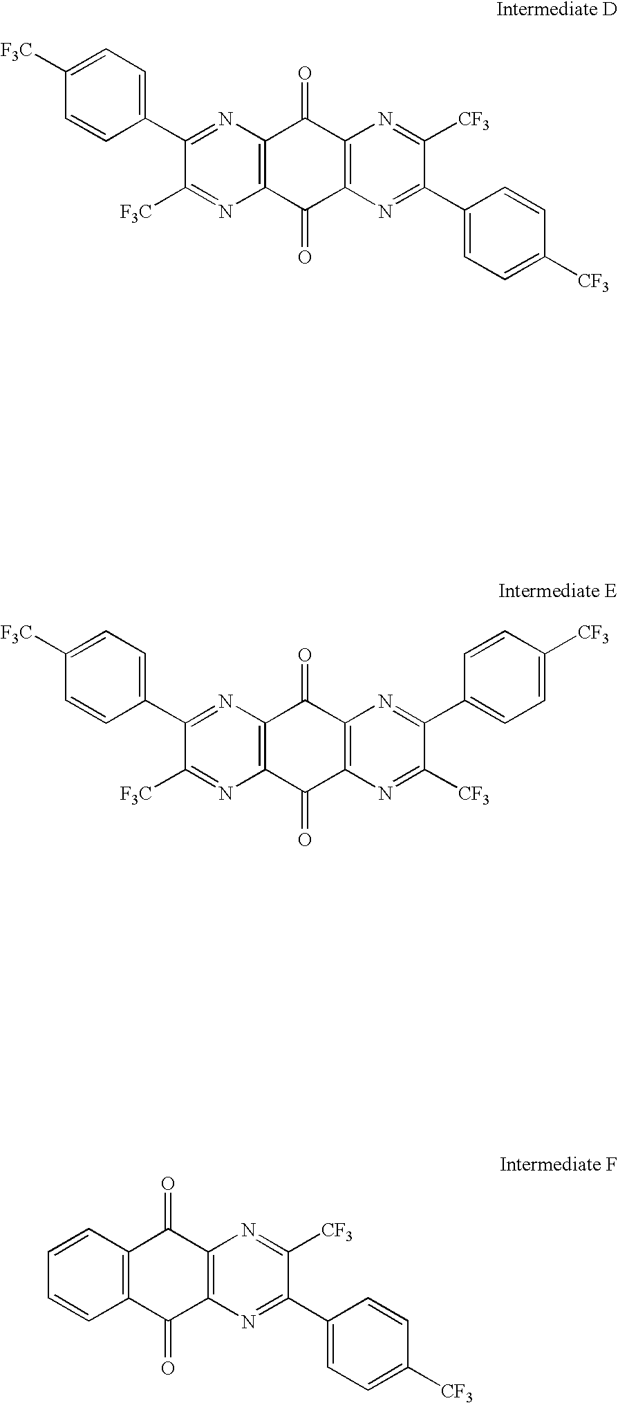


| TABLE 1 | ||||
| Material of | Driving | |||
| Hole-injecting layer | voltage (V) | Half life (hr) | ||
| Example 6 | Formula (A-3) | 6.1 | 7,800 |
| Formula (C-1) | |||
| Example 7 | Formula (A-8) | 6.4 | 8,700 |
| Example 8 | Formula (A-21) | 5.8 | 7,000 |
| Formula (A-22) | |||
| Example 9 | Formula (B-14) | 5.9 | 6,500 |
| Comparative | Formula (C-1) | 6.6 | 5,000 |
| Example 2 | |||

| TABLE 2 | ||||
| Material of | ||||
| Hole-injecting | Luminous | |||
| layer | Driving voltage (V) | efficiency (Cd/A) | ||
| Example 10 | Formula (A-3) | 6.1 | 2.2 |
| Example 11 | Formula (A-8) | 6.0 | 2.3 |
| Comparative | Formula (C-1) | 15.6 | 0.2 |
| Example 3 | |||
| Comparative | Intermediate A | 13.9 | 0.3 |
| Example 4 | |||
Claims (16)


Applications Claiming Priority (3)
| Application Number | Priority Date | Filing Date | Title |
|---|---|---|---|
| JP2007138870 | 2007-05-25 | ||
| JP2007-138870 | 2007-05-25 | ||
| PCT/JP2008/059303 WO2008146665A1 (en) | 2007-05-25 | 2008-05-21 | Material for organic electroluminescent device, organic electroluminescent device, and organic electroluminescent display device |
Publications (2)
| Publication Number | Publication Date |
|---|---|
| US20100181555A1 US20100181555A1 (en) | 2010-07-22 |
| US8044390B2 true US8044390B2 (en) | 2011-10-25 |
Family
ID=40074924
Family Applications (1)
| Application Number | Title | Priority Date | Filing Date |
|---|---|---|---|
| US12/601,808 Active 2027-09-29 US8044390B2 (en) | 2007-05-25 | 2007-05-21 | Material for organic electroluminescent device, organic electroluminescent device, and organic electroluminescent display |
Country Status (4)
| Country | Link |
|---|---|
| US (1) | US8044390B2 (en) |
| JP (1) | JP5523096B2 (en) |
| TW (1) | TW200913342A (en) |
| WO (1) | WO2008146665A1 (en) |
Cited By (57)
| Publication number | Priority date | Publication date | Assignee | Title |
|---|---|---|---|---|
| US20110111520A1 (en) * | 2008-05-08 | 2011-05-12 | Bard Allen J | Luminescent nanostructured materials for use in electrogenerated chemiluminescence |
| US20110120891A1 (en) * | 2008-04-11 | 2011-05-26 | Fan Fu-Ren F | Method and apparatus for nanoparticle electrogenerated chemiluminescence amplification |
| WO2013083216A1 (en) | 2011-11-17 | 2013-06-13 | Merck Patent Gmbh | Spiro dihydroacridine derivatives and the use thereof as materials for organic electroluminescence devices |
| WO2013120577A1 (en) | 2012-02-14 | 2013-08-22 | Merck Patent Gmbh | Spirobifluorene compounds for organic electroluminescent devices |
| WO2013135352A1 (en) | 2012-03-15 | 2013-09-19 | Merck Patent Gmbh | Electronic devices |
| WO2013182263A1 (en) | 2012-06-06 | 2013-12-12 | Merck Patent Gmbh | Phenanthrene compounds for organic electronic devices |
| WO2014044344A1 (en) | 2012-09-18 | 2014-03-27 | Merck Patent Gmbh | Materials for electronic devices |
| WO2014067614A1 (en) | 2012-10-31 | 2014-05-08 | Merck Patent Gmbh | Electronic device |
| WO2014106522A1 (en) | 2013-01-03 | 2014-07-10 | Merck Patent Gmbh | Materials for electronic devices |
| WO2015036080A1 (en) | 2013-09-11 | 2015-03-19 | Merck Patent Gmbh | Organic electroluminescent device |
| WO2015139808A1 (en) | 2014-03-18 | 2015-09-24 | Merck Patent Gmbh | Organic electroluminescent device |
| WO2016091353A1 (en) | 2014-12-12 | 2016-06-16 | Merck Patent Gmbh | Organic compounds with soluble groups |
| WO2017012687A1 (en) | 2015-07-22 | 2017-01-26 | Merck Patent Gmbh | Materials for organic electroluminescent devices |
| WO2017028940A1 (en) | 2015-08-14 | 2017-02-23 | Merck Patent Gmbh | Phenoxazine derivatives for organic electroluminescent devices |
| WO2017133829A1 (en) | 2016-02-05 | 2017-08-10 | Merck Patent Gmbh | Materials for electronic devices |
| WO2017207596A1 (en) | 2016-06-03 | 2017-12-07 | Merck Patent Gmbh | Materials for organic electroluminescent devices |
| DE102017008794A1 (en) | 2016-10-17 | 2018-04-19 | Merck Patent Gmbh | Materials for use in electronic devices |
| WO2018069167A1 (en) | 2016-10-10 | 2018-04-19 | Merck Patent Gmbh | Electronic device |
| WO2018083053A1 (en) | 2016-11-02 | 2018-05-11 | Merck Patent Gmbh | Materials for electronic devices |
| WO2018087020A1 (en) | 2016-11-08 | 2018-05-17 | Merck Patent Gmbh | Compounds for electronic devices |
| WO2018095940A1 (en) | 2016-11-25 | 2018-05-31 | Merck Patent Gmbh | Bisbenzofuran-fused indeno[1,2-b]fluorene derivatives and related compounds as materials for organic electroluminescent devices (oled) |
| WO2018095888A1 (en) | 2016-11-25 | 2018-05-31 | Merck Patent Gmbh | Bisbenzofuran-fused 2,8-diaminoindeno[1,2-b]fluorene derivatives and related compounds as materials for organic electroluminescent devices (oled) |
| WO2018141706A1 (en) | 2017-02-02 | 2018-08-09 | Merck Patent Gmbh | Materials for electronic devices |
| WO2018157981A1 (en) | 2017-03-02 | 2018-09-07 | Merck Patent Gmbh | Materials for organic electronic devices |
| EP3378857A1 (en) | 2012-11-12 | 2018-09-26 | Merck Patent GmbH | Materials for electronic devices |
| WO2018234346A1 (en) | 2017-06-23 | 2018-12-27 | Merck Patent Gmbh | Materials for organic electroluminescent devices |
| WO2019002190A1 (en) | 2017-06-28 | 2019-01-03 | Merck Patent Gmbh | Materials for electronic devices |
| WO2019020654A1 (en) | 2017-07-28 | 2019-01-31 | Merck Patent Gmbh | Spirobifluorene derivatives for use in electronic devices |
| WO2019048443A1 (en) | 2017-09-08 | 2019-03-14 | Merck Patent Gmbh | Materials for electronic devices |
| WO2019076789A1 (en) | 2017-10-17 | 2019-04-25 | Merck Patent Gmbh | Materials for organic electroluminescent devices |
| WO2019101833A1 (en) | 2017-11-24 | 2019-05-31 | Merck Patent Gmbh | Materials for organic electroluminescent devices |
| WO2019101719A1 (en) | 2017-11-23 | 2019-05-31 | Merck Patent Gmbh | Materials for electronic devices |
| WO2019101835A1 (en) | 2017-11-24 | 2019-05-31 | Merck Patent Gmbh | Materials for organic electroluminescent devices |
| WO2019115577A1 (en) | 2017-12-15 | 2019-06-20 | Merck Patent Gmbh | Substituted aromatic amines for use in organic electroluminescent devices |
| WO2019121483A1 (en) | 2017-12-20 | 2019-06-27 | Merck Patent Gmbh | Heteroaromatic compounds |
| WO2019170572A1 (en) | 2018-03-06 | 2019-09-12 | Merck Patent Gmbh | Materials for organic electroluminescent devices |
| WO2019170578A1 (en) | 2018-03-06 | 2019-09-12 | Merck Patent Gmbh | Materials for organic electroluminescent devices |
| WO2019175149A1 (en) | 2018-03-16 | 2019-09-19 | Merck Patent Gmbh | Materials for organic electroluminescent devices |
| WO2020043657A1 (en) | 2018-08-28 | 2020-03-05 | Merck Patent Gmbh | Materials for organic electroluminescent devices |
| WO2020043646A1 (en) | 2018-08-28 | 2020-03-05 | Merck Patent Gmbh | Materials for organic electroluminescent devices |
| WO2020043640A1 (en) | 2018-08-28 | 2020-03-05 | Merck Patent Gmbh | Materials for organic electroluminescent devices |
| WO2020053150A1 (en) | 2018-09-12 | 2020-03-19 | Merck Patent Gmbh | Materials for organic electroluminescent devices |
| WO2020089138A1 (en) | 2018-10-31 | 2020-05-07 | Merck Patent Gmbh | Materials for organic electroluminescent devices |
| WO2021110741A1 (en) | 2019-12-04 | 2021-06-10 | Merck Patent Gmbh | Materials for organic electroluminescent devices |
| WO2022017997A1 (en) | 2020-07-22 | 2022-01-27 | Merck Patent Gmbh | Materials for organic electroluminescent devices |
| WO2023052275A1 (en) | 2021-09-28 | 2023-04-06 | Merck Patent Gmbh | Materials for electronic devices |
| WO2023052272A1 (en) | 2021-09-28 | 2023-04-06 | Merck Patent Gmbh | Materials for electronic devices |
| WO2023052314A1 (en) | 2021-09-28 | 2023-04-06 | Merck Patent Gmbh | Materials for electronic devices |
| WO2023052313A1 (en) | 2021-09-28 | 2023-04-06 | Merck Patent Gmbh | Materials for electronic devices |
| WO2023094412A1 (en) | 2021-11-25 | 2023-06-01 | Merck Patent Gmbh | Materials for electronic devices |
| WO2023117835A1 (en) | 2021-12-21 | 2023-06-29 | Merck Patent Gmbh | Electronic devices |
| WO2023117836A1 (en) | 2021-12-21 | 2023-06-29 | Merck Patent Gmbh | Electronic devices |
| WO2023117837A1 (en) | 2021-12-21 | 2023-06-29 | Merck Patent Gmbh | Process for preparing deuterated organic compounds |
| WO2023152346A1 (en) | 2022-02-14 | 2023-08-17 | Merck Patent Gmbh | Materials for electronic devices |
| EP4236652A2 (en) | 2015-07-29 | 2023-08-30 | Merck Patent GmbH | Materials for organic electroluminescent devices |
| WO2023222559A1 (en) | 2022-05-18 | 2023-11-23 | Merck Patent Gmbh | Process for preparing deuterated organic compounds |
| WO2024013004A1 (en) | 2022-07-11 | 2024-01-18 | Merck Patent Gmbh | Materials for electronic devices |
Families Citing this family (6)
| Publication number | Priority date | Publication date | Assignee | Title |
|---|---|---|---|---|
| JP2009021104A (en) * | 2007-07-12 | 2009-01-29 | Sumitomo Chemical Co Ltd | Manufacturing method for organic light emitting element |
| DE102008061843B4 (en) * | 2008-12-15 | 2018-01-18 | Novaled Gmbh | Heterocyclic compounds and their use in electronic and optoelectronic devices |
| KR101477613B1 (en) * | 2009-03-31 | 2014-12-30 | 롬엔드하스전자재료코리아유한회사 | Novel Compounds for Organic Electronic Material and Organic Electronic Device Using the Same |
| KR102174919B1 (en) * | 2013-12-03 | 2020-11-05 | 엘지디스플레이 주식회사 | Organic Light Emitting Diode and Organic Light Emitting Display Device Using the Same |
| KR101730537B1 (en) | 2015-11-30 | 2017-04-26 | 엘지디스플레이 주식회사 | Display device and method for manufacturing the same |
| JP6601557B2 (en) * | 2016-04-25 | 2019-11-06 | 京セラドキュメントソリューションズ株式会社 | Electrophotographic photosensitive member, process cartridge, and image forming apparatus |
Citations (20)
| Publication number | Priority date | Publication date | Assignee | Title |
|---|---|---|---|---|
| JPS60115575A (en) | 1983-10-19 | 1985-06-22 | バスフ アクチェン ゲゼルシャフト | Electric charge transfer comple |
| JPS6232465A (en) | 1985-08-05 | 1987-02-12 | Toshio Mukai | Organic electrophotographic material |
| US4720432A (en) | 1987-02-11 | 1988-01-19 | Eastman Kodak Company | Electroluminescent device with organic luminescent medium |
| JPH0242449A (en) | 1988-08-02 | 1990-02-13 | Minolta Camera Co Ltd | Photosensitive body |
| JPH02214866A (en) | 1988-12-21 | 1990-08-27 | Eastman Kodak Co | Electrophotographic element containing certain anthraquinone derivative as electron transporter |
| US5061569A (en) | 1990-07-26 | 1991-10-29 | Eastman Kodak Company | Electroluminescent device with organic electroluminescent medium |
| US5077142A (en) | 1989-04-20 | 1991-12-31 | Ricoh Company, Ltd. | Electroluminescent devices |
| JPH04297076A (en) | 1991-01-31 | 1992-10-21 | Toshiba Corp | Organic el element |
| JPH093342A (en) | 1995-06-22 | 1997-01-07 | Chisso Corp | Pyrazinoquinoxaline derivative, its production, and organic electroluminescent element |
| JPH11251067A (en) | 1998-03-02 | 1999-09-17 | Junji Kido | Organic electroluminescence element |
| JP2000109717A (en) | 1998-10-01 | 2000-04-18 | Reiko Udagawa | Anthraquinone compound and electrophotographic photoreceptor using the same |
| JP2000196140A (en) | 1998-12-28 | 2000-07-14 | Sharp Corp | Organic electroluminescence element and fabrication thereof |
| JP2001297883A (en) | 2000-04-17 | 2001-10-26 | Mitsubishi Chemicals Corp | Organic electric-field light emission element |
| JP2003031365A (en) | 2001-05-02 | 2003-01-31 | Junji Kido | Organic electroluminescent element |
| JP2004514257A (en) | 2000-11-20 | 2004-05-13 | ノヴァレッド・ゲゼルシャフト・ミト・ベシュレンクテル・ハフツング | Light emitting device with organic layer |
| US20040113547A1 (en) | 1999-12-31 | 2004-06-17 | Se-Hwan Son | Electroluminescent devices with low work function anode |
| JP2005167175A (en) | 2003-12-04 | 2005-06-23 | Novaled Gmbh | Method for doping organic semiconductor with quinone diimine derivative |
| US20050255334A1 (en) | 2004-05-11 | 2005-11-17 | Minsoo Kang | Organic electronic device |
| US20070090756A1 (en) | 2005-10-11 | 2007-04-26 | Fujifilm Corporation | Organic electroluminescent element |
| US7538341B2 (en) * | 1999-12-31 | 2009-05-26 | Lg Chem, Ltd. | Electronic device comprising organic compound having p-type semiconducting characteristics |
-
2007
- 2007-05-21 US US12/601,808 patent/US8044390B2/en active Active
-
2008
- 2008-05-21 JP JP2009516259A patent/JP5523096B2/en active Active
- 2008-05-21 WO PCT/JP2008/059303 patent/WO2008146665A1/en active Application Filing
- 2008-05-23 TW TW097119266A patent/TW200913342A/en unknown
Patent Citations (20)
| Publication number | Priority date | Publication date | Assignee | Title |
|---|---|---|---|---|
| JPS60115575A (en) | 1983-10-19 | 1985-06-22 | バスフ アクチェン ゲゼルシャフト | Electric charge transfer comple |
| JPS6232465A (en) | 1985-08-05 | 1987-02-12 | Toshio Mukai | Organic electrophotographic material |
| US4720432A (en) | 1987-02-11 | 1988-01-19 | Eastman Kodak Company | Electroluminescent device with organic luminescent medium |
| JPH0242449A (en) | 1988-08-02 | 1990-02-13 | Minolta Camera Co Ltd | Photosensitive body |
| JPH02214866A (en) | 1988-12-21 | 1990-08-27 | Eastman Kodak Co | Electrophotographic element containing certain anthraquinone derivative as electron transporter |
| US5077142A (en) | 1989-04-20 | 1991-12-31 | Ricoh Company, Ltd. | Electroluminescent devices |
| US5061569A (en) | 1990-07-26 | 1991-10-29 | Eastman Kodak Company | Electroluminescent device with organic electroluminescent medium |
| JPH04297076A (en) | 1991-01-31 | 1992-10-21 | Toshiba Corp | Organic el element |
| JPH093342A (en) | 1995-06-22 | 1997-01-07 | Chisso Corp | Pyrazinoquinoxaline derivative, its production, and organic electroluminescent element |
| JPH11251067A (en) | 1998-03-02 | 1999-09-17 | Junji Kido | Organic electroluminescence element |
| JP2000109717A (en) | 1998-10-01 | 2000-04-18 | Reiko Udagawa | Anthraquinone compound and electrophotographic photoreceptor using the same |
| JP2000196140A (en) | 1998-12-28 | 2000-07-14 | Sharp Corp | Organic electroluminescence element and fabrication thereof |
| US20040113547A1 (en) | 1999-12-31 | 2004-06-17 | Se-Hwan Son | Electroluminescent devices with low work function anode |
| US7538341B2 (en) * | 1999-12-31 | 2009-05-26 | Lg Chem, Ltd. | Electronic device comprising organic compound having p-type semiconducting characteristics |
| JP2001297883A (en) | 2000-04-17 | 2001-10-26 | Mitsubishi Chemicals Corp | Organic electric-field light emission element |
| JP2004514257A (en) | 2000-11-20 | 2004-05-13 | ノヴァレッド・ゲゼルシャフト・ミト・ベシュレンクテル・ハフツング | Light emitting device with organic layer |
| JP2003031365A (en) | 2001-05-02 | 2003-01-31 | Junji Kido | Organic electroluminescent element |
| JP2005167175A (en) | 2003-12-04 | 2005-06-23 | Novaled Gmbh | Method for doping organic semiconductor with quinone diimine derivative |
| US20050255334A1 (en) | 2004-05-11 | 2005-11-17 | Minsoo Kang | Organic electronic device |
| US20070090756A1 (en) | 2005-10-11 | 2007-04-26 | Fujifilm Corporation | Organic electroluminescent element |
Non-Patent Citations (3)
| Title |
|---|
| C.W. Tang et al., Organic Electroluminescent Diodes, Applied Physics Letters, Sep. 21, 1987, vol. 51, No. 12, pp. 913-915. |
| T. Suzuki, Single-Component Organic Semiconductors Based on Novel Radicals that Exhibit Electrochemical Amphotericity: Preparation, Crystal Structures, and Solid-State Properties of N, N′-Dicyanopyrazinonaphathoquinodiiminides Substitute with an N-Alkylpyridiminum Unit, Journal of Organic Chemistry, Jan. 12, 2001, vol. 66, No. 1, pp. 216-224. |
| T. Suzuki, Single-Component Organic Semiconductors Based on Novel Radicals that Exhibit Electrochemical Amphotericity: Preparation, Crystal Structures, and Solid-State Properties of N, N'-Dicyanopyrazinonaphathoquinodiiminides Substitute with an N-Alkylpyridiminum Unit, Journal of Organic Chemistry, Jan. 12, 2001, vol. 66, No. 1, pp. 216-224. |
Cited By (70)
| Publication number | Priority date | Publication date | Assignee | Title |
|---|---|---|---|---|
| US20110120891A1 (en) * | 2008-04-11 | 2011-05-26 | Fan Fu-Ren F | Method and apparatus for nanoparticle electrogenerated chemiluminescence amplification |
| US9086370B2 (en) | 2008-04-11 | 2015-07-21 | Board Of Regents Of The University Of Texas System | Method for nanoparticle electrogenerated chemiluminescence amplification |
| US8586378B2 (en) | 2008-04-11 | 2013-11-19 | Board Of Regents, The University Of Texas System | Method and apparatus for nanoparticle electrogenerated chemiluminescence amplification |
| US8815159B2 (en) | 2008-05-08 | 2014-08-26 | Board Of Regents Of The University Of Texas System | Luminescent nanostructured materials for use in electrogenerated chemiluminescence |
| US8372652B2 (en) | 2008-05-08 | 2013-02-12 | Board Of Regents Of The University Of Texas System | Luminescent nanostructured materials for use in electrogenerated chemiluminescence |
| US20110111520A1 (en) * | 2008-05-08 | 2011-05-12 | Bard Allen J | Luminescent nanostructured materials for use in electrogenerated chemiluminescence |
| US9346997B2 (en) | 2008-05-08 | 2016-05-24 | Board Of Regents Of The University Of Texas System | Luminescent nanostructured materials for use in electrogenerated chemiluminescence |
| WO2013083216A1 (en) | 2011-11-17 | 2013-06-13 | Merck Patent Gmbh | Spiro dihydroacridine derivatives and the use thereof as materials for organic electroluminescence devices |
| EP3235892A1 (en) | 2012-02-14 | 2017-10-25 | Merck Patent GmbH | Materials for organic electroluminescent devices |
| EP3101088A1 (en) | 2012-02-14 | 2016-12-07 | Merck Patent GmbH | Materials for organic electroluminescent devices |
| WO2013120577A1 (en) | 2012-02-14 | 2013-08-22 | Merck Patent Gmbh | Spirobifluorene compounds for organic electroluminescent devices |
| EP3460864A1 (en) | 2012-03-15 | 2019-03-27 | Merck Patent GmbH | Electronic devices |
| WO2013135352A1 (en) | 2012-03-15 | 2013-09-19 | Merck Patent Gmbh | Electronic devices |
| WO2013182263A1 (en) | 2012-06-06 | 2013-12-12 | Merck Patent Gmbh | Phenanthrene compounds for organic electronic devices |
| WO2014044344A1 (en) | 2012-09-18 | 2014-03-27 | Merck Patent Gmbh | Materials for electronic devices |
| WO2014067614A1 (en) | 2012-10-31 | 2014-05-08 | Merck Patent Gmbh | Electronic device |
| EP3806176A1 (en) | 2012-10-31 | 2021-04-14 | Merck Patent GmbH | Electronic device |
| EP3378857A1 (en) | 2012-11-12 | 2018-09-26 | Merck Patent GmbH | Materials for electronic devices |
| WO2014106522A1 (en) | 2013-01-03 | 2014-07-10 | Merck Patent Gmbh | Materials for electronic devices |
| WO2015036080A1 (en) | 2013-09-11 | 2015-03-19 | Merck Patent Gmbh | Organic electroluminescent device |
| WO2015139808A1 (en) | 2014-03-18 | 2015-09-24 | Merck Patent Gmbh | Organic electroluminescent device |
| WO2016091353A1 (en) | 2014-12-12 | 2016-06-16 | Merck Patent Gmbh | Organic compounds with soluble groups |
| WO2017012687A1 (en) | 2015-07-22 | 2017-01-26 | Merck Patent Gmbh | Materials for organic electroluminescent devices |
| EP4236652A2 (en) | 2015-07-29 | 2023-08-30 | Merck Patent GmbH | Materials for organic electroluminescent devices |
| WO2017028940A1 (en) | 2015-08-14 | 2017-02-23 | Merck Patent Gmbh | Phenoxazine derivatives for organic electroluminescent devices |
| WO2017133829A1 (en) | 2016-02-05 | 2017-08-10 | Merck Patent Gmbh | Materials for electronic devices |
| EP3978477A2 (en) | 2016-06-03 | 2022-04-06 | Merck Patent GmbH | Materials for organic electroluminescent devices |
| WO2017207596A1 (en) | 2016-06-03 | 2017-12-07 | Merck Patent Gmbh | Materials for organic electroluminescent devices |
| EP4113643A1 (en) | 2016-10-10 | 2023-01-04 | Merck Patent GmbH | Electronic device |
| WO2018069167A1 (en) | 2016-10-10 | 2018-04-19 | Merck Patent Gmbh | Electronic device |
| EP4255151A2 (en) | 2016-10-10 | 2023-10-04 | Merck Patent GmbH | Spiro[fluorene-9,9'-(thio)xanthene] compounds |
| DE102017008794A1 (en) | 2016-10-17 | 2018-04-19 | Merck Patent Gmbh | Materials for use in electronic devices |
| WO2018083053A1 (en) | 2016-11-02 | 2018-05-11 | Merck Patent Gmbh | Materials for electronic devices |
| WO2018087020A1 (en) | 2016-11-08 | 2018-05-17 | Merck Patent Gmbh | Compounds for electronic devices |
| WO2018095940A1 (en) | 2016-11-25 | 2018-05-31 | Merck Patent Gmbh | Bisbenzofuran-fused indeno[1,2-b]fluorene derivatives and related compounds as materials for organic electroluminescent devices (oled) |
| WO2018095888A1 (en) | 2016-11-25 | 2018-05-31 | Merck Patent Gmbh | Bisbenzofuran-fused 2,8-diaminoindeno[1,2-b]fluorene derivatives and related compounds as materials for organic electroluminescent devices (oled) |
| WO2018141706A1 (en) | 2017-02-02 | 2018-08-09 | Merck Patent Gmbh | Materials for electronic devices |
| WO2018157981A1 (en) | 2017-03-02 | 2018-09-07 | Merck Patent Gmbh | Materials for organic electronic devices |
| WO2018234346A1 (en) | 2017-06-23 | 2018-12-27 | Merck Patent Gmbh | Materials for organic electroluminescent devices |
| WO2019002190A1 (en) | 2017-06-28 | 2019-01-03 | Merck Patent Gmbh | Materials for electronic devices |
| WO2019020654A1 (en) | 2017-07-28 | 2019-01-31 | Merck Patent Gmbh | Spirobifluorene derivatives for use in electronic devices |
| WO2019048443A1 (en) | 2017-09-08 | 2019-03-14 | Merck Patent Gmbh | Materials for electronic devices |
| WO2019076789A1 (en) | 2017-10-17 | 2019-04-25 | Merck Patent Gmbh | Materials for organic electroluminescent devices |
| WO2019101719A1 (en) | 2017-11-23 | 2019-05-31 | Merck Patent Gmbh | Materials for electronic devices |
| EP4242286A2 (en) | 2017-11-23 | 2023-09-13 | Merck Patent GmbH | Materials for electronic devices |
| WO2019101833A1 (en) | 2017-11-24 | 2019-05-31 | Merck Patent Gmbh | Materials for organic electroluminescent devices |
| WO2019101835A1 (en) | 2017-11-24 | 2019-05-31 | Merck Patent Gmbh | Materials for organic electroluminescent devices |
| WO2019115577A1 (en) | 2017-12-15 | 2019-06-20 | Merck Patent Gmbh | Substituted aromatic amines for use in organic electroluminescent devices |
| WO2019121483A1 (en) | 2017-12-20 | 2019-06-27 | Merck Patent Gmbh | Heteroaromatic compounds |
| WO2019170572A1 (en) | 2018-03-06 | 2019-09-12 | Merck Patent Gmbh | Materials for organic electroluminescent devices |
| WO2019170578A1 (en) | 2018-03-06 | 2019-09-12 | Merck Patent Gmbh | Materials for organic electroluminescent devices |
| WO2019175149A1 (en) | 2018-03-16 | 2019-09-19 | Merck Patent Gmbh | Materials for organic electroluminescent devices |
| WO2020043640A1 (en) | 2018-08-28 | 2020-03-05 | Merck Patent Gmbh | Materials for organic electroluminescent devices |
| WO2020043657A1 (en) | 2018-08-28 | 2020-03-05 | Merck Patent Gmbh | Materials for organic electroluminescent devices |
| WO2020043646A1 (en) | 2018-08-28 | 2020-03-05 | Merck Patent Gmbh | Materials for organic electroluminescent devices |
| WO2020053150A1 (en) | 2018-09-12 | 2020-03-19 | Merck Patent Gmbh | Materials for organic electroluminescent devices |
| WO2020089138A1 (en) | 2018-10-31 | 2020-05-07 | Merck Patent Gmbh | Materials for organic electroluminescent devices |
| WO2021110741A1 (en) | 2019-12-04 | 2021-06-10 | Merck Patent Gmbh | Materials for organic electroluminescent devices |
| WO2022017997A1 (en) | 2020-07-22 | 2022-01-27 | Merck Patent Gmbh | Materials for organic electroluminescent devices |
| WO2023052272A1 (en) | 2021-09-28 | 2023-04-06 | Merck Patent Gmbh | Materials for electronic devices |
| WO2023052313A1 (en) | 2021-09-28 | 2023-04-06 | Merck Patent Gmbh | Materials for electronic devices |
| WO2023052314A1 (en) | 2021-09-28 | 2023-04-06 | Merck Patent Gmbh | Materials for electronic devices |
| WO2023052275A1 (en) | 2021-09-28 | 2023-04-06 | Merck Patent Gmbh | Materials for electronic devices |
| WO2023094412A1 (en) | 2021-11-25 | 2023-06-01 | Merck Patent Gmbh | Materials for electronic devices |
| WO2023117835A1 (en) | 2021-12-21 | 2023-06-29 | Merck Patent Gmbh | Electronic devices |
| WO2023117836A1 (en) | 2021-12-21 | 2023-06-29 | Merck Patent Gmbh | Electronic devices |
| WO2023117837A1 (en) | 2021-12-21 | 2023-06-29 | Merck Patent Gmbh | Process for preparing deuterated organic compounds |
| WO2023152346A1 (en) | 2022-02-14 | 2023-08-17 | Merck Patent Gmbh | Materials for electronic devices |
| WO2023222559A1 (en) | 2022-05-18 | 2023-11-23 | Merck Patent Gmbh | Process for preparing deuterated organic compounds |
| WO2024013004A1 (en) | 2022-07-11 | 2024-01-18 | Merck Patent Gmbh | Materials for electronic devices |
Also Published As
| Publication number | Publication date |
|---|---|
| WO2008146665A1 (en) | 2008-12-04 |
| JP5523096B2 (en) | 2014-06-18 |
| JPWO2008146665A1 (en) | 2010-08-19 |
| TW200913342A (en) | 2009-03-16 |
| US20100181555A1 (en) | 2010-07-22 |
Similar Documents
| Publication | Publication Date | Title |
|---|---|---|
| US8044390B2 (en) | Material for organic electroluminescent device, organic electroluminescent device, and organic electroluminescent display | |
| US8481177B2 (en) | Material for organic electroluminescence device and organic electroluminescence device | |
| US8372527B2 (en) | Material for organic electroluminescent element, and organic electroluminescent element | |
| US8088901B2 (en) | Azaindenofluorenedione derivative, material for organic electroluminescence device and organic electroluminescence device | |
| US8119828B2 (en) | Material for an organic electroluminescence device and an organic electroluminescence device | |
| US8076839B2 (en) | Organic electroluminescence device | |
| US8168327B2 (en) | Imide derivative, material for organic electroluminescent device and organic electroluminescent device using the same | |
| US20080093985A1 (en) | Material for organic electroluminescent device and organic electroluminescent device using the same | |
| US20090243473A1 (en) | Organic electroluminescence device | |
| US20080193796A1 (en) | Organic electroluminescent device | |
| JP5097700B2 (en) | Organic electroluminescence device |
Legal Events
| Date | Code | Title | Description |
|---|---|---|---|
| AS | Assignment |
Owner name: IDEMITSU KOSAN CO., LTD., JAPAN Free format text: ASSIGNMENT OF ASSIGNORS INTEREST;ASSIGNORS:HOSOKAWA, CHISHIO;MORISHITA, HIRONOBU;YOSHINAGA, TADAHIKO;AND OTHERS;SIGNING DATES FROM 20091110 TO 20091129;REEL/FRAME:023664/0266 Owner name: SONY CORPORATION, JAPAN Free format text: ASSIGNMENT OF ASSIGNORS INTEREST;ASSIGNORS:HOSOKAWA, CHISHIO;MORISHITA, HIRONOBU;YOSHINAGA, TADAHIKO;AND OTHERS;SIGNING DATES FROM 20091110 TO 20091129;REEL/FRAME:023664/0266 |
|
| STCF | Information on status: patent grant |
Free format text: PATENTED CASE |
|
| CC | Certificate of correction | ||
| CC | Certificate of correction | ||
| FPAY | Fee payment |
Year of fee payment: 4 |
|
| AS | Assignment |
Owner name: JOLED INC., JAPAN Free format text: ASSIGNMENT OF ASSIGNORS INTEREST;ASSIGNOR:SONY CORPORATION;REEL/FRAME:043477/0926 Effective date: 20170725 |
|
| MAFP | Maintenance fee payment |
Free format text: PAYMENT OF MAINTENANCE FEE, 8TH YEAR, LARGE ENTITY (ORIGINAL EVENT CODE: M1552); ENTITY STATUS OF PATENT OWNER: LARGE ENTITY Year of fee payment: 8 |
|
| MAFP | Maintenance fee payment |
Free format text: PAYMENT OF MAINTENANCE FEE, 12TH YEAR, LARGE ENTITY (ORIGINAL EVENT CODE: M1553); ENTITY STATUS OF PATENT OWNER: LARGE ENTITY Year of fee payment: 12 |