US8040984B2 - Methods and apparatus for improved jitter tolerance in an SFP limit amplified signal - Google Patents
Methods and apparatus for improved jitter tolerance in an SFP limit amplified signal Download PDFInfo
- Publication number
- US8040984B2 US8040984B2 US11/967,602 US96760207A US8040984B2 US 8040984 B2 US8040984 B2 US 8040984B2 US 96760207 A US96760207 A US 96760207A US 8040984 B2 US8040984 B2 US 8040984B2
- Authority
- US
- United States
- Prior art keywords
- pass filter
- low pass
- received signal
- data eye
- output
- Prior art date
- Legal status (The legal status is an assumption and is not a legal conclusion. Google has not performed a legal analysis and makes no representation as to the accuracy of the status listed.)
- Expired - Fee Related, expires
Links
Images


Classifications
-
- H—ELECTRICITY
- H04—ELECTRIC COMMUNICATION TECHNIQUE
- H04B—TRANSMISSION
- H04B10/00—Transmission systems employing electromagnetic waves other than radio-waves, e.g. infrared, visible or ultraviolet light, or employing corpuscular radiation, e.g. quantum communication
- H04B10/60—Receivers
- H04B10/66—Non-coherent receivers, e.g. using direct detection
- H04B10/69—Electrical arrangements in the receiver
- H04B10/697—Arrangements for reducing noise and distortion
- H04B10/6972—Arrangements for reducing noise and distortion using passive filtering
-
- H—ELECTRICITY
- H04—ELECTRIC COMMUNICATION TECHNIQUE
- H04B—TRANSMISSION
- H04B1/00—Details of transmission systems, not covered by a single one of groups H04B3/00 - H04B13/00; Details of transmission systems not characterised by the medium used for transmission
- H04B1/06—Receivers
- H04B1/10—Means associated with receiver for limiting or suppressing noise or interference
-
- H—ELECTRICITY
- H04—ELECTRIC COMMUNICATION TECHNIQUE
- H04L—TRANSMISSION OF DIGITAL INFORMATION, e.g. TELEGRAPHIC COMMUNICATION
- H04L25/00—Baseband systems
- H04L25/02—Details ; arrangements for supplying electrical power along data transmission lines
- H04L25/08—Modifications for reducing interference; Modifications for reducing effects due to line faults ; Receiver end arrangements for detecting or overcoming line faults
Definitions
- the present invention is related to techniques for processing a received signal in a communication system and, more particularly, to techniques for improving jitter tolerance in a received signal.
- Digital communication receivers typically must sample an incoming waveform and then reliably detect the sampled data. Signals traveling through a dispersive medium typically suffer from group delay and attenuation. The group delay creates pulse spreading, inter-symbol interference and other noise.
- communication receivers often employ well-known filtering, amplification and equalization techniques. For example, zero equalization or decision-feedback equalization (DFE) techniques (or both) are often employed.
- DFE decision-feedback equalization
- Such equalization techniques are widely-used for removing intersymbol interference and to improve the noise margin. See, for example, R. Gitlin et al., Digital Communication Principles, (Plenum Press, 1992) and E. A. Lee and D. G. Messerschmitt, Digital Communications, (Kluwer Academic Press, 1988), each incorporated by reference herein.
- Communication receivers also often amplify a received signal with a small form factor pluggable (SFP) limiting amplifier.
- SFP small form factor pluggable
- jitter tolerance is improved in a communications receiver by applying a received signal to an SFP limiting amplifier; and applying an output of the SFP limiting amplifier to a low pass filter to improve the jitter tolerance.
- the low pass filter optionally applies a programmable amount of attenuation to high frequency components of the output.
- the low pass filter can optionally be applied by a pre-amplifier in the communications receiver.
- the low pass filter slew rate controls (i.e., rotates) a data eye representation of the received signal to increase the data eye representation along a time axis. In this manner, the time margin and jitter tolerance of the received signal are improved.
- the noise margin of the received signal can optionally be improved by applying an output of the low pass filter to an all pass filter.
- the data eye representation is a single-sided data eye representation. The single-sided data eye representation only contains transitions from a first binary value to a binary value of 0 or 1.
- a slew rate controller can evaluate the data eye statistics to determine a setting for the low pass filter.
- FIG. 1 is a block diagram of a communication system in which the present invention can operate
- FIGS. 2A and 2B illustrate the transfer characteristics of the first and second stages, respectively, of the pre-amplifier of FIG. 1 ;
- FIGS. 3A and 3B illustrate the received signal that is applied to the SFP limiting amplifier of FIG. 1 ;
- FIGS. 4A and 4B illustrate the output of the SFP limiting amplifier of FIG. 1 ;
- FIG. 5A illustrates the reduced (uncorrected) jitter tolerance at the output of the SFP limiting amplifier of FIG. 1
- FIGS. 5B-5C illustrate moderate jitter tolerance correction and severe jitter tolerance correction, respectively, in accordance with the present invention.
- FIG. 1 is a block diagram of a communication system 100 .
- a transmitter 110 transmits data over a channel 120 for receipt by a receiver 130 .
- the channel 120 can be any dispersive channel, such as a backplane, an optical link or an electrical connection, or a combination of the foregoing.
- Pre-emphasis techniques are optionally applied in the transmitter 210 before the signal is transmitted over the channel 120 .
- equalization techniques (not shown), such as zero equalization and/or decision feedback equalization (DFE) are optionally applied in the receiver 130 .
- DFE decision feedback equalization
- the receiver 130 includes an SFP limiting amplifier 150 and a pre-amplifier 160 , in a known manner.
- the transfer characteristics of the pre-amplifier 160 are discussed further below in conjunction with FIGS. 2A and 2B .
- the received signal that is applied to the SFP limiting amplifier 150 is discussed further below in conjunction with FIGS. 3A and 3B .
- the output of the SFP limiting amplifier 150 is discussed further below in conjunction with FIGS. 4A and 4B .
- the present invention recognizes that when the dispersive signal passes through the SFP limiting amplifier 150 , the output of SFP limiting amplifier 150 exhibits pulse width shrinkage (PWS) resulting in loss of jitter tolerance.
- PWS pulse width shrinkage
- the pre-amplifier 160 filters the output of the SFP limiting amplifier 150 to improve the jitter tolerance, as discussed further below in conjunction with FIGS. 5A , 5 B and 5 C.
- a first stage of the pre-amplifier 160 applies a low pass filter
- a second stage of the pre-amplifier 160 optionally applies a high frequency boost.
- the receiver 130 also includes a data and eye detector 170 for recovering the transmitted information.
- the data and eye detector 170 may be embodied, for example, using the data eye monitoring techniques described, for example, in U.S. patent application Ser. No. 11/540,946, filed Sep. 29, 2006, entitled “Method And Apparatus For Determining Latch Position For Decision-Feedback Equalization Using Single-Sided Eye,” incorporated by reference herein.
- the data eye statistics generated by the data and eye detector 170 are processed by a slew rate controller 175 to evaluate the PWS and determine an appropriate zero control correction value.
- the zero control correction value will apply an appropriate amount of low pass filtering to offset the measured PWS.
- the slew rate controller 175 may be embodied, for example, using the slew rate control techniques described in U.S. patent application Ser. No. 11/367,964, filed Mar. 3, 2006, entitled “Method and Apparatus for Slew Rate Control,” incorporated by reference herein, as modified herein to provide slew rate control using low pass filtering.
- FIGS. 2A and 2B illustrate the transfer characteristics 200 , 250 (amplitude as a function of frequency) of the first and second stages, respectively, of the pre-amplifier 160 .
- the pre-amplifier 160 trades off between high frequency and low frequency transfer characteristics. If a high frequency boost is applied, the low frequency boost is lost and vise versa.
- the exemplary pre-amplifier 160 provides 16 “settings” of filter options ( 0 - 15 ) in the first stage Setting 0 applies the most low pass filtering (relative to the other settings) to attenuate the high frequency components of the applied signal.
- Setting 15 applies high pass filtering to attenuate the low frequency components. As shown in FIG.
- the pre-amplifier 160 in the second stage, provides a high frequency boost.
- the pre-amplifier 160 employs low frequency attenuation and high frequency gain for equalization.
- the present invention employs moderate to severe low pass filtering to attenutate the high frequency components and maintain the low frequency components) in the first stage of the pre-amplifier 160 in order to improve the jitter tolerance.
- FIGS. 3A and 3B illustrate the received signal that is applied to the SFP limiting amplifier 150 .
- FIG. 3A illustrates a classical data eye view 300 of the received signal
- FIG. 3B illustrates a DFE data eye view 350 of the received signal.
- the data eye views 300 , 350 can be obtained, for example, from a data eye monitor, such as those described in U.S. patent application Ser. No. 11/540,946, filed Sep. 29, 2006, entitled “Method And Apparatus For Determining Latch Position For Decision-Feedback Equalization Using Single-Sided Eye,” incorporated by reference herein.
- a DFE data eye view also referred to as a single-sided eye view, opens up the data eye by containing only transitions from one binary value (i.e., only 1 ⁇ x or 0 ⁇ x transitions).
- the DFE data eye view extracts a larger DFE eye by constraining the data to only contain signal transitions from, for example, a binary value 1 to a binary value of 0 or 1 (referred to as 1 ⁇ x), and inhibiting any signal transitions from a binary value of 0.
- FIGS. 4A and 4B illustrate the output of the SFP limiting amplifier 150 .
- FIG. 4A illustrates a classical data eye view 400 of the SFP limited signal and
- FIG. 4B illustrates a DFE data eye view 450 of the SFP limited signal.
- the output 400 , 450 of the SFP limiting amplifier 150 exhibits pulse width shrinkage resulting in loss of jitter tolerance.
- the pulse width would approximately correspond to line 410 without pulse shrinkage, but the shrinkage from the SFP limiting amplifier 150 causes the pulse width to approximately correspond to line 420 .
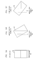
- FIG. 5A illustrates the reduced (uncorrected) jitter tolerance at the output of the SFP limiting amplifier 150
- FIGS. 5B-5C illustrate moderate jitter tolerance correction and severe jitter tolerance correction, respectively, in accordance with the present invention.
- an exemplary data eye 500 at the output of the SFP limiting amplifier 150 exhibits pulse width shrinkage and has a jitter tolerance 510 corresponding to the width of the data eye 500 .
- FIG. 5B corresponds to moderate jitter tolerance correction by applying moderate low pass filtering in the first stage of pre-amplifier 160 , such as setting 5 of FIG. 2A .
- the low pass filtering will expand the data eye 520 in the time domain by rotating the data eye 520 , as shown in FIG. 5B (at the cost of vertical separation (noise margin), as discussed further below).
- the data eye 520 rotates to the left, as shown in FIG. 5B , the horizontal spacing increases and is limited by the length of the diagonal length.
- the improvement in the jitter tolerance 530 corresponds to the increased spacing in the horizontal (time) direction.
- the rotation shown in FIG. 5B can be considered to decrease the Nyquist signal magnitude response and thereby slew rate limit the Nyquist signal, causing the rotation of the NRZ signal DFE eye and the increased jitter margin.
- FIG. 5C corresponds to more severe jitter tolerance correction by applying severe low pass filtering in the first stage of pre-amplifier 160 , such as setting 0 of FIG. 2A .
- the low pass filtering will further expand the data eye 550 in the time domain by further rotating the data eye 550 , as shown in FIG. 5C (again at the cost of vertical separation (noise margin), as discussed further below).
- the horizontal spacing further increases and is limited by the length of the diagonal length.
- the improvement in the jitter tolerance 560 corresponds to the increased spacing in the horizontal (time) direction.
- a second stage of the pre-amplifier 160 optionally applies a high frequency boost to assert an all pass DC gain and to open up the vertical separation.
- the functions of the present invention can be embodied in the form of methods and apparatuses for practicing those methods.
- One or more aspects of the present invention can be embodied in the form of program code, fob example, whether stored in a storage medium, loaded into and/or executed by a machine, or transmitted over some transmission medium, wherein, when the program code is loaded into and executed by a machine, such as a computer, the machine becomes an apparatus for practicing the invention.
- program code segments combine with the processor to provide a device that operates analogously to specific logic circuits.
Landscapes
- Engineering & Computer Science (AREA)
- Computer Networks & Wireless Communication (AREA)
- Signal Processing (AREA)
- Physics & Mathematics (AREA)
- Electromagnetism (AREA)
- Power Engineering (AREA)
- Dc Digital Transmission (AREA)
- Circuits Of Receivers In General (AREA)
- Cable Transmission Systems, Equalization Of Radio And Reduction Of Echo (AREA)
Abstract
Description
Claims (20)
Priority Applications (6)
| Application Number | Priority Date | Filing Date | Title |
|---|---|---|---|
| US11/967,602 US8040984B2 (en) | 2007-12-31 | 2007-12-31 | Methods and apparatus for improved jitter tolerance in an SFP limit amplified signal |
| JP2008329105A JP5627850B2 (en) | 2007-12-31 | 2008-12-25 | Method and apparatus for improving jitter tolerance of SFP limited amplified signal |
| CNA2008101902905A CN101478323A (en) | 2007-12-31 | 2008-12-30 | Methods and apparatus for improved jitter tolerance in an SFP limit amplified signal |
| EP08173111A EP2075930A1 (en) | 2007-12-31 | 2008-12-30 | Methods and apparatus for improved jitter tolerance in an SFP limit amplified signal |
| KR1020080136480A KR101457221B1 (en) | 2007-12-31 | 2008-12-30 | Methods and apparatus for improved jitter tolerance in an sfp limit amplified signal |
| TW097151863A TWI445364B (en) | 2007-12-31 | 2008-12-31 | Methods and apparatus for improved jitter tolerance in an sfp limit amplified signal |
Applications Claiming Priority (1)
| Application Number | Priority Date | Filing Date | Title |
|---|---|---|---|
| US11/967,602 US8040984B2 (en) | 2007-12-31 | 2007-12-31 | Methods and apparatus for improved jitter tolerance in an SFP limit amplified signal |
Publications (2)
| Publication Number | Publication Date |
|---|---|
| US20090168940A1 US20090168940A1 (en) | 2009-07-02 |
| US8040984B2 true US8040984B2 (en) | 2011-10-18 |
Family
ID=40550550
Family Applications (1)
| Application Number | Title | Priority Date | Filing Date |
|---|---|---|---|
| US11/967,602 Expired - Fee Related US8040984B2 (en) | 2007-12-31 | 2007-12-31 | Methods and apparatus for improved jitter tolerance in an SFP limit amplified signal |
Country Status (6)
| Country | Link |
|---|---|
| US (1) | US8040984B2 (en) |
| EP (1) | EP2075930A1 (en) |
| JP (1) | JP5627850B2 (en) |
| KR (1) | KR101457221B1 (en) |
| CN (1) | CN101478323A (en) |
| TW (1) | TWI445364B (en) |
Cited By (1)
| Publication number | Priority date | Publication date | Assignee | Title |
|---|---|---|---|---|
| US8737549B2 (en) | 2012-04-30 | 2014-05-27 | Lsi Corporation | Receiver having limiter-enhanced data eye openings |
Families Citing this family (1)
| Publication number | Priority date | Publication date | Assignee | Title |
|---|---|---|---|---|
| US8422891B2 (en) * | 2010-09-24 | 2013-04-16 | Intel Corporation | Jitter reduction of electrical signals from limiting optical modules |
Citations (5)
| Publication number | Priority date | Publication date | Assignee | Title |
|---|---|---|---|---|
| EP1187373A2 (en) | 2000-09-05 | 2002-03-13 | Samsung Electronics Co., Ltd. | Bit rate detection circuit and algorithm for optical networks |
| US20020085656A1 (en) | 2000-08-30 | 2002-07-04 | Lee Sang-Hyun | Data recovery using data eye tracking |
| US20030137355A1 (en) * | 2002-01-18 | 2003-07-24 | Lin Allan Ming-Lun | Method and circuit for controlling power amplifiers |
| WO2006032628A1 (en) | 2004-09-21 | 2006-03-30 | Bookham Technology Plc | Optical communication modules |
| US20070050805A1 (en) | 2005-08-29 | 2007-03-01 | Sergiu Rotenstein | Transmission of pathological data patterns |
Family Cites Families (6)
| Publication number | Priority date | Publication date | Assignee | Title |
|---|---|---|---|---|
| GB1187373A (en) * | 1966-10-05 | 1970-04-08 | Graviner Colnbrook Ltd | Improvements in or relating to Explosive Cartridges |
| JPS6464411A (en) * | 1987-09-04 | 1989-03-10 | Kenwood Corp | Receiver for digital signal processing system |
| JPH0730445A (en) * | 1993-07-12 | 1995-01-31 | Sony Corp | Receiver |
| JPH0991876A (en) * | 1995-09-22 | 1997-04-04 | Sony Corp | Signal reproduction circuit |
| JP2002135340A (en) * | 2000-10-25 | 2002-05-10 | Ando Electric Co Ltd | Waveform shaping circuit |
| JP4531090B2 (en) * | 2005-03-18 | 2010-08-25 | 富士通株式会社 | Jitter suppression circuit |
-
2007
- 2007-12-31 US US11/967,602 patent/US8040984B2/en not_active Expired - Fee Related
-
2008
- 2008-12-25 JP JP2008329105A patent/JP5627850B2/en not_active Expired - Fee Related
- 2008-12-30 CN CNA2008101902905A patent/CN101478323A/en active Pending
- 2008-12-30 EP EP08173111A patent/EP2075930A1/en not_active Withdrawn
- 2008-12-30 KR KR1020080136480A patent/KR101457221B1/en not_active Expired - Fee Related
- 2008-12-31 TW TW097151863A patent/TWI445364B/en not_active IP Right Cessation
Patent Citations (6)
| Publication number | Priority date | Publication date | Assignee | Title |
|---|---|---|---|---|
| US20020085656A1 (en) | 2000-08-30 | 2002-07-04 | Lee Sang-Hyun | Data recovery using data eye tracking |
| EP1187373A2 (en) | 2000-09-05 | 2002-03-13 | Samsung Electronics Co., Ltd. | Bit rate detection circuit and algorithm for optical networks |
| US6684033B1 (en) * | 2000-09-05 | 2004-01-27 | Samsung Electronics Co., Ltd. | Bit rate detection circuit and algorithm for optical networks |
| US20030137355A1 (en) * | 2002-01-18 | 2003-07-24 | Lin Allan Ming-Lun | Method and circuit for controlling power amplifiers |
| WO2006032628A1 (en) | 2004-09-21 | 2006-03-30 | Bookham Technology Plc | Optical communication modules |
| US20070050805A1 (en) | 2005-08-29 | 2007-03-01 | Sergiu Rotenstein | Transmission of pathological data patterns |
Non-Patent Citations (3)
| Title |
|---|
| HFDN-22.0, "Configuring the MAX 3861 AGC AMP as an SFP Limiting amplifier with RSSI," Maxim Integrated products, pp. 1-6, Apr. 2008. * |
| Kucharski et al., "Jitter Considerations in the Design of a 10-Gb/s Automatic Gain Control Amplifier," IEEE Transactions on Microwave Theory and Techniques, vol. 53, No. 2, pp. 590-597 (Feb. 1, 2005). |
| Matsuura et al., "Performance Improvement of Optical RZ-Receiver by Utilizing Semiconductor-Based Waveform Converter," Lasers and Electro-Optics Society, 17th Annual Meeting of the IEEE, vol. 1, pp. 392-393 (Nov. 11, 2008). |
Cited By (2)
| Publication number | Priority date | Publication date | Assignee | Title |
|---|---|---|---|---|
| US8737549B2 (en) | 2012-04-30 | 2014-05-27 | Lsi Corporation | Receiver having limiter-enhanced data eye openings |
| US9294314B2 (en) | 2012-04-30 | 2016-03-22 | Avago Technologies General Ip (Singapore) Pte. Ltd. | Receiver having limiter-enhanced data eye openings |
Also Published As
| Publication number | Publication date |
|---|---|
| TWI445364B (en) | 2014-07-11 |
| EP2075930A1 (en) | 2009-07-01 |
| JP2009165123A (en) | 2009-07-23 |
| CN101478323A (en) | 2009-07-08 |
| US20090168940A1 (en) | 2009-07-02 |
| KR20090073982A (en) | 2009-07-03 |
| KR101457221B1 (en) | 2014-10-31 |
| TW200943755A (en) | 2009-10-16 |
| JP5627850B2 (en) | 2014-11-19 |
Similar Documents
| Publication | Publication Date | Title |
|---|---|---|
| US7623600B2 (en) | High speed receive equalizer architecture | |
| US9294314B2 (en) | Receiver having limiter-enhanced data eye openings | |
| US9025655B1 (en) | Transmitter training using receiver equalizer coefficients | |
| US7769110B2 (en) | Threshold adjust system and method | |
| US9385897B2 (en) | Methods and apparatus for adapting transmitter equalization coefficients based on receiver gain adaptation | |
| KR101131643B1 (en) | Continuous time-decision feedback equalizer | |
| US20150256364A1 (en) | Group delay based back channel post cursor adaptation | |
| US20060045176A1 (en) | System and method for digital adaptive equalization with failure detection and recovery | |
| US8369470B2 (en) | Methods and apparatus for adapting one or more equalization parameters by reducing group delay spread | |
| US7702053B2 (en) | State based algorithm to minimize mean squared error | |
| US8432959B2 (en) | Method and apparatus for equalization using one or more qualifiers | |
| US9130792B2 (en) | Closed-loop high-speed channel equalizer adaptation | |
| US8040984B2 (en) | Methods and apparatus for improved jitter tolerance in an SFP limit amplified signal | |
| US8483266B2 (en) | Methods and apparatus for adaptation of continuous time-decision feedback equalizers with programmable adaptation patterns | |
| US8315298B2 (en) | Method and apparatus for rate-dependent equalization | |
| US7269216B2 (en) | Blind magnitude equalizer for segment sync-based timing recovery of receivers | |
| US8259784B2 (en) | High-speed continuous-time feedback equalizer for serial link receiver | |
| EP3217618B1 (en) | Signal compensation method and device | |
| US7656977B2 (en) | Method and system of frequency domain equalization | |
| CN119892569A (en) | CTLE self-adaptive equalization method, system, medium and device based on hybrid equalization | |
| KR20030022362A (en) | Pre-equalizer correcting the magnitude of a received signal without regard to phase distortions |
Legal Events
| Date | Code | Title | Description |
|---|---|---|---|
| AS | Assignment |
Owner name: AGERE SYSTEMS INC., PENNSYLVANIA Free format text: ASSIGNMENT OF ASSIGNORS INTEREST;ASSIGNORS:AZIZ, PERVEZ M.;HEALEY, ADAM B.;MOBIN, MOHAMMAD S.;AND OTHERS;REEL/FRAME:020784/0834;SIGNING DATES FROM 20080110 TO 20080410 Owner name: AGERE SYSTEMS INC., PENNSYLVANIA Free format text: ASSIGNMENT OF ASSIGNORS INTEREST;ASSIGNORS:AZIZ, PERVEZ M.;HEALEY, ADAM B.;MOBIN, MOHAMMAD S.;AND OTHERS;SIGNING DATES FROM 20080110 TO 20080410;REEL/FRAME:020784/0834 |
|
| CC | Certificate of correction | ||
| AS | Assignment |
Owner name: DEUTSCHE BANK AG NEW YORK BRANCH, AS COLLATERAL AG Free format text: PATENT SECURITY AGREEMENT;ASSIGNORS:LSI CORPORATION;AGERE SYSTEMS LLC;REEL/FRAME:032856/0031 Effective date: 20140506 Owner name: DEUTSCHE BANK AG NEW YORK BRANCH, AS COLLATERAL AGENT, NEW YORK Free format text: PATENT SECURITY AGREEMENT;ASSIGNORS:LSI CORPORATION;AGERE SYSTEMS LLC;REEL/FRAME:032856/0031 Effective date: 20140506 |
|
| AS | Assignment |
Owner name: AVAGO TECHNOLOGIES GENERAL IP (SINGAPORE) PTE. LTD., SINGAPORE Free format text: ASSIGNMENT OF ASSIGNORS INTEREST;ASSIGNOR:AGERE SYSTEMS LLC;REEL/FRAME:035365/0634 Effective date: 20140804 Owner name: AVAGO TECHNOLOGIES GENERAL IP (SINGAPORE) PTE. LTD Free format text: ASSIGNMENT OF ASSIGNORS INTEREST;ASSIGNOR:AGERE SYSTEMS LLC;REEL/FRAME:035365/0634 Effective date: 20140804 |
|
| REMI | Maintenance fee reminder mailed | ||
| LAPS | Lapse for failure to pay maintenance fees | ||
| STCH | Information on status: patent discontinuation |
Free format text: PATENT EXPIRED DUE TO NONPAYMENT OF MAINTENANCE FEES UNDER 37 CFR 1.362 |
|
| STCH | Information on status: patent discontinuation |
Free format text: PATENT EXPIRED DUE TO NONPAYMENT OF MAINTENANCE FEES UNDER 37 CFR 1.362 |
|
| FP | Lapsed due to failure to pay maintenance fee |
Effective date: 20151018 |
|
| AS | Assignment |
Owner name: LSI CORPORATION, CALIFORNIA Free format text: TERMINATION AND RELEASE OF SECURITY INTEREST IN PATENT RIGHTS (RELEASES RF 032856-0031);ASSIGNOR:DEUTSCHE BANK AG NEW YORK BRANCH, AS COLLATERAL AGENT;REEL/FRAME:037684/0039 Effective date: 20160201 Owner name: AGERE SYSTEMS LLC, PENNSYLVANIA Free format text: TERMINATION AND RELEASE OF SECURITY INTEREST IN PATENT RIGHTS (RELEASES RF 032856-0031);ASSIGNOR:DEUTSCHE BANK AG NEW YORK BRANCH, AS COLLATERAL AGENT;REEL/FRAME:037684/0039 Effective date: 20160201 |