US8039376B2 - Methods of changing threshold voltages of semiconductor transistors by ion implantation - Google Patents
Methods of changing threshold voltages of semiconductor transistors by ion implantation Download PDFInfo
- Publication number
- US8039376B2 US8039376B2 US11/939,578 US93957807A US8039376B2 US 8039376 B2 US8039376 B2 US 8039376B2 US 93957807 A US93957807 A US 93957807A US 8039376 B2 US8039376 B2 US 8039376B2
- Authority
- US
- United States
- Prior art keywords
- dopants
- dose
- layer
- body region
- adjustment
- Prior art date
- Legal status (The legal status is an assumption and is not a legal conclusion. Google has not performed a legal analysis and makes no representation as to the accuracy of the status listed.)
- Expired - Fee Related, expires
Links
- 238000000034 method Methods 0.000 title claims abstract description 105
- 239000004065 semiconductor Substances 0.000 title claims abstract description 83
- 238000005468 ion implantation Methods 0.000 title description 8
- 210000000746 body region Anatomy 0.000 claims abstract description 114
- 239000002019 doping agent Substances 0.000 claims abstract description 92
- 238000002513 implantation Methods 0.000 claims abstract description 71
- 239000000758 substrate Substances 0.000 claims abstract description 42
- 238000010849 ion bombardment Methods 0.000 claims abstract description 18
- 238000000059 patterning Methods 0.000 claims abstract description 18
- 229920002120 photoresistant polymer Polymers 0.000 claims description 65
- XUIMIQQOPSSXEZ-UHFFFAOYSA-N Silicon Chemical compound [Si] XUIMIQQOPSSXEZ-UHFFFAOYSA-N 0.000 claims description 44
- 229910052710 silicon Inorganic materials 0.000 claims description 44
- 239000010703 silicon Substances 0.000 claims description 44
- VYPSYNLAJGMNEJ-UHFFFAOYSA-N Silicium dioxide Chemical compound O=[Si]=O VYPSYNLAJGMNEJ-UHFFFAOYSA-N 0.000 claims description 10
- 238000004519 manufacturing process Methods 0.000 claims description 8
- 235000012239 silicon dioxide Nutrition 0.000 claims description 5
- 239000000377 silicon dioxide Substances 0.000 claims description 5
- 230000000903 blocking effect Effects 0.000 description 10
- 150000002500 ions Chemical class 0.000 description 6
- 239000007943 implant Substances 0.000 description 5
- 238000001039 wet etching Methods 0.000 description 3
- 238000005229 chemical vapour deposition Methods 0.000 description 2
- 238000012986 modification Methods 0.000 description 2
- 230000004048 modification Effects 0.000 description 2
- 229910000577 Silicon-germanium Inorganic materials 0.000 description 1
- LEVVHYCKPQWKOP-UHFFFAOYSA-N [Si].[Ge] Chemical compound [Si].[Ge] LEVVHYCKPQWKOP-UHFFFAOYSA-N 0.000 description 1
- 230000015572 biosynthetic process Effects 0.000 description 1
- 238000007796 conventional method Methods 0.000 description 1
- 230000005669 field effect Effects 0.000 description 1
- 239000012212 insulator Substances 0.000 description 1
- 238000002955 isolation Methods 0.000 description 1
- 230000001590 oxidative effect Effects 0.000 description 1
Images


Classifications
-
- H—ELECTRICITY
- H01—ELECTRIC ELEMENTS
- H01L—SEMICONDUCTOR DEVICES NOT COVERED BY CLASS H10
- H01L21/00—Processes or apparatus adapted for the manufacture or treatment of semiconductor or solid state devices or of parts thereof
- H01L21/02—Manufacture or treatment of semiconductor devices or of parts thereof
- H01L21/04—Manufacture or treatment of semiconductor devices or of parts thereof the devices having at least one potential-jump barrier or surface barrier, e.g. PN junction, depletion layer or carrier concentration layer
- H01L21/18—Manufacture or treatment of semiconductor devices or of parts thereof the devices having at least one potential-jump barrier or surface barrier, e.g. PN junction, depletion layer or carrier concentration layer the devices having semiconductor bodies comprising elements of Group IV of the Periodic System or AIIIBV compounds with or without impurities, e.g. doping materials
- H01L21/26—Bombardment with radiation
- H01L21/263—Bombardment with radiation with high-energy radiation
- H01L21/265—Bombardment with radiation with high-energy radiation producing ion implantation
- H01L21/26586—Bombardment with radiation with high-energy radiation producing ion implantation characterised by the angle between the ion beam and the crystal planes or the main crystal surface
-
- H—ELECTRICITY
- H01—ELECTRIC ELEMENTS
- H01L—SEMICONDUCTOR DEVICES NOT COVERED BY CLASS H10
- H01L21/00—Processes or apparatus adapted for the manufacture or treatment of semiconductor or solid state devices or of parts thereof
- H01L21/70—Manufacture or treatment of devices consisting of a plurality of solid state components formed in or on a common substrate or of parts thereof; Manufacture of integrated circuit devices or of parts thereof
- H01L21/77—Manufacture or treatment of devices consisting of a plurality of solid state components or integrated circuits formed in, or on, a common substrate
- H01L21/78—Manufacture or treatment of devices consisting of a plurality of solid state components or integrated circuits formed in, or on, a common substrate with subsequent division of the substrate into plural individual devices
- H01L21/82—Manufacture or treatment of devices consisting of a plurality of solid state components or integrated circuits formed in, or on, a common substrate with subsequent division of the substrate into plural individual devices to produce devices, e.g. integrated circuits, each consisting of a plurality of components
- H01L21/822—Manufacture or treatment of devices consisting of a plurality of solid state components or integrated circuits formed in, or on, a common substrate with subsequent division of the substrate into plural individual devices to produce devices, e.g. integrated circuits, each consisting of a plurality of components the substrate being a semiconductor, using silicon technology
- H01L21/8232—Field-effect technology
- H01L21/8234—MIS technology, i.e. integration processes of field effect transistors of the conductor-insulator-semiconductor type
- H01L21/823431—MIS technology, i.e. integration processes of field effect transistors of the conductor-insulator-semiconductor type with a particular manufacturing method of transistors with a horizontal current flow in a vertical sidewall of a semiconductor body, e.g. FinFET, MuGFET
-
- H—ELECTRICITY
- H01—ELECTRIC ELEMENTS
- H01L—SEMICONDUCTOR DEVICES NOT COVERED BY CLASS H10
- H01L29/00—Semiconductor devices adapted for rectifying, amplifying, oscillating or switching, or capacitors or resistors with at least one potential-jump barrier or surface barrier, e.g. PN junction depletion layer or carrier concentration layer; Details of semiconductor bodies or of electrodes thereof ; Multistep manufacturing processes therefor
- H01L29/02—Semiconductor bodies ; Multistep manufacturing processes therefor
- H01L29/06—Semiconductor bodies ; Multistep manufacturing processes therefor characterised by their shape; characterised by the shapes, relative sizes, or dispositions of the semiconductor regions ; characterised by the concentration or distribution of impurities within semiconductor regions
- H01L29/10—Semiconductor bodies ; Multistep manufacturing processes therefor characterised by their shape; characterised by the shapes, relative sizes, or dispositions of the semiconductor regions ; characterised by the concentration or distribution of impurities within semiconductor regions with semiconductor regions connected to an electrode not carrying current to be rectified, amplified or switched and such electrode being part of a semiconductor device which comprises three or more electrodes
- H01L29/1025—Channel region of field-effect devices
- H01L29/1029—Channel region of field-effect devices of field-effect transistors
- H01L29/1033—Channel region of field-effect devices of field-effect transistors with insulated gate, e.g. characterised by the length, the width, the geometric contour or the doping structure
- H01L29/105—Channel region of field-effect devices of field-effect transistors with insulated gate, e.g. characterised by the length, the width, the geometric contour or the doping structure with vertical doping variation
-
- H—ELECTRICITY
- H01—ELECTRIC ELEMENTS
- H01L—SEMICONDUCTOR DEVICES NOT COVERED BY CLASS H10
- H01L29/00—Semiconductor devices adapted for rectifying, amplifying, oscillating or switching, or capacitors or resistors with at least one potential-jump barrier or surface barrier, e.g. PN junction depletion layer or carrier concentration layer; Details of semiconductor bodies or of electrodes thereof ; Multistep manufacturing processes therefor
- H01L29/66—Types of semiconductor device ; Multistep manufacturing processes therefor
- H01L29/66007—Multistep manufacturing processes
- H01L29/66075—Multistep manufacturing processes of devices having semiconductor bodies comprising group 14 or group 13/15 materials
- H01L29/66227—Multistep manufacturing processes of devices having semiconductor bodies comprising group 14 or group 13/15 materials the devices being controllable only by the electric current supplied or the electric potential applied, to an electrode which does not carry the current to be rectified, amplified or switched, e.g. three-terminal devices
- H01L29/66409—Unipolar field-effect transistors
- H01L29/66477—Unipolar field-effect transistors with an insulated gate, i.e. MISFET
- H01L29/66787—Unipolar field-effect transistors with an insulated gate, i.e. MISFET with a gate at the side of the channel
- H01L29/66795—Unipolar field-effect transistors with an insulated gate, i.e. MISFET with a gate at the side of the channel with a horizontal current flow in a vertical sidewall of a semiconductor body, e.g. FinFET, MuGFET
- H01L29/66803—Unipolar field-effect transistors with an insulated gate, i.e. MISFET with a gate at the side of the channel with a horizontal current flow in a vertical sidewall of a semiconductor body, e.g. FinFET, MuGFET with a step of doping the vertical sidewall, e.g. using tilted or multi-angled implants
Definitions
- the present invention relates generally to methods for changing threshold voltages of transistors and more particularly to methods for changing threshold voltages of transistors by ion implantation.
- the semiconductor body of the transistor can be doped with dopants by ion implantation. Control of the value of the threshold voltage is critical to good performance and low power consumption of the circuits employing the transistors.
- MoGFETs Multi-Gate FETs
- doping the MuGFET body is best performed with angled implants at some point following fin (body) formation, as this allows total dose delivery to the body to be minimally affected by incidental variations in fin dimensions.
- the spacing between two FETs with differing threshold voltages can be as close, physically, as two such FETs having the same threshold voltage; this provides for high circuit density and low manufacturing cost.
- this spacing is such that the blocking resist used to allow such threshold-adjusting implants into one FET and not an adjacent one, prohibits the use of tilted, or angled, implants that are needed to dope the fins in a uniform manner. Therefore, there is always a need for a method of changing the threshold voltage of a transistor that is better than that of the prior art.
- the present invention provides a semiconductor structure fabrication method, comprising providing a semiconductor structure which includes a semiconductor substrate, wherein the semiconductor substrate includes a top substrate surface which defines a reference direction perpendicular to the top substrate surface and pointing from outside to inside of the semiconductor substrate, and wherein the semiconductor substrate further includes a semiconductor body region; then implanting an adjustment dose of dopants of a first doping polarity into the semiconductor body region by an adjustment implantation process, wherein ion bombardment of the adjustment implantation process is in the reference direction; then patterning the semiconductor substrate resulting in side walls of the semiconductor body region being exposed to a surrounding ambient; and then implanting a base dose of dopants of a second doping polarity into the semiconductor body region by a base implantation process, wherein ion bombardment of the base implantation process is in a direction which makes a non-zero angle with the reference direction.
- the present invention provides a method of changing the threshold voltage of a transistor that is better than that of the prior art.
- FIGS. 1A-1M show cross-section views used to illustrate a fabrication process of a semiconductor structure, in accordance with embodiments of the present invention.
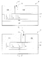
- FIGS. 1A-1M show cross-section views used to illustrate a fabrication process of a semiconductor structure 100 , in accordance with embodiments of the present invention. More specifically, with reference to FIG. 1A , the fabrication process of the semiconductor structure 100 starts with an SOI (Silicon On Insulator) substrate 110 + 120 + 130 .
- the SOI substrate 110 + 120 + 130 comprises a silicon substrate 110 , a BOX (buried oxide) layer 120 on top of the silicon substrate 110 , and an active silicon layer 130 on top of the BOX layer 120 .
- the SOI substrate 110 + 120 + 130 can be formed by a conventional method.
- the substrate can comprise a conventional (bulk) silicon wafer, and furthermore, may further comprise an isolation layer comprising either doped silicon or silicon-germanium in lieu of the BOX layer 120 .
- FETs field effect transistors
- a first FET not shown
- a second FET not shown
- a third FET not shown
- Vt 1 , Vt 2 , and Vt 3 threshold voltages
- Vt 1 , Vt 2 , and Vt 3 are achieved by, among other things, individually doping the body regions 131 , 132 , and 133 , respectively.
- Dp 1 , Dp 2 , and Dp 3 be the three doses of p-type dopants that need to be implanted into the body regions 131 , 132 , and 133 to achieve ⁇ Vt 1 , ⁇ Vt 2 , and ⁇ Vt 3 , respectively. It should be noted that a dose of dopants in a body region is the number of dopant atoms that are implanted into the body region. Also, let Db be a first base dose of p-type dopants, wherein Db>0, Db ⁇ Dp 1 , Db ⁇ Dp 2 , and Db ⁇ Dp 3 .
- the first base dose, Db can directly achieve one of the desired values of Vt, in which case no adjustment implant (i.e. an adjustment dose of value zero) is employed.
- Da 1 , Da 2 , and Da 3 are implanted into the body regions 131 , 132 , and 133 by individual first, second, and third adjustment Vt implantation processes, respectively, whereas Db is implanted into each of the body regions 131 , 132 , and 133 by a same first base Vt implantation process.
- a fourth FET (not shown), a fifth FET (not shown), and a sixth FET (not shown) having threshold voltages Vt 4 , Vt 5 , and Vt 6 are to be formed on body regions 134 , 135 , and 136 of the active silicon layer 130 , respectively.
- Vt 4 , Vt 5 , and Vt 6 are achieved by, among other things, individually doping the body regions 134 , 135 , and 136 , respectively.
- the threshold voltages of the fourth, fifth, and sixth FETs would be Vt 04 , Vt 05 , and Vt 06 , respectively.
- ⁇ Vt 4 , ⁇ Vt 5 , and ⁇ Vt 6 can be achieved by implanting p-type dopants in the body regions 134 , 135 , and 136 , respectively.
- Dp 4 , Dp 5 , and Dp 6 be the three doses of p-type dopants that need to be implanted into the body regions 134 , 135 , and 136 to achieve ⁇ Vt 4 , ⁇ Vt 5 , and ⁇ Vt 6 , respectively.
- Db′ be a second base dose of p-type dopants, wherein Db′>0, Db′ ⁇ Dp 4 , Db′ ⁇ Dp 5 , and Db′ ⁇ Dp 6 .
- Da 4 , Da 5 , and Da 6 are implanted into the body regions 134 , 135 , and 136 by individual fourth, fifth, and sixth adjustment Vt implantation processes, respectively, whereas Db′ is implanted into each of the body regions 134 , 135 , and 136 by a same second base Vt implantation process.
- the implantation processes described above can be carried out in detail as follows.
- a pad film 140 is formed on top of the active silicon layer 130 .
- the pad film 140 can comprise silicon dioxide.
- the pad film 140 can be formed by (i) CVD (Chemical Vapor Deposition) of silicon dioxide on top of the active silicon layer 130 or (ii) thermally oxidizing the top surface of the active silicon layer 130 resulting in the pad film 140 on top of the active silicon layer 130 .
- a photoresist layer 150 a is formed on top of the pad film 140 .
- the photoresist layer 150 a can be formed by a spin-on process followed by baking.
- the photoresist layer 150 a is patterned resulting in a photoresist trench 151 in the photoresist layer 150 a such that the entire body region 131 overlaps the photoresist trench 151 in a direction defined by an arrow 151 ′ (also called a direction 151 ′) which is perpendicular to the top surface 137 of the active silicon layer 130 .
- an arrow 151 ′ also called a direction 151 ′
- the other body regions 132 , 133 , 134 , 135 , and 136 FIG.
- the body region 131 is doped with p-type dopants by the first adjustment Vt implantation process such that Da 1 is implanted into the body region 131 . More specifically, the body region 131 is doped by implanting p-type dopants into the body region 131 with the patterned photoresist layer 150 a as a blocking mask. In one embodiment, the bombarding direction of the first adjustment Vt implantation process is in the direction 151 ′.
- the first adjustment Vt implantation process hereafter is referred to as the first adjustment Vt implantation process 151 ′.
- an ion implantation process and the arrow representing the direction of the ion bombardment of the ion implantation process have the same reference numeral for simplicity.
- the photoresist layer 150 a is removed by wet etching.
- the body region 131 is doped with Da 1 by performing the first adjustment Vt implantation process 151 ′ through the photoresist trench 151 using the patterned photoresist layer 150 a as a blocking mask.
- the body region 132 is doped with Da 2 .
- the body region 132 is doped with Da 2 in a manner similar to the manner in which the body region 131 is doped with Da 1 in FIG. 1C . More specifically, the body region 132 is doped with Da 2 by performing the second adjustment Vt implantation process 152 ′ through a photoresist trench 152 using a patterned photoresist layer 150 b as a blocking mask.
- the body region 133 is doped with Da 3 .
- the body region 133 is doped with Da 3 in a manner similar to the manner in which the body region 131 is doped with Da 1 in FIG. 1C . More specifically, the body region 133 is doped with Da 3 by performing the third adjustment Vt implantation process 153 ′ through a photoresist trench 153 using a patterned photoresist layer 150 c as a blocking mask.
- the body region 134 is doped with Da 4 .
- the body region 134 is doped with Da 4 in a manner similar to the manner in which the body region 131 is doped with Da 1 in FIG. 1C . More specifically, the body region 134 is doped with Da 4 by performing the fourth adjustment Vt implantation process 154 ′ through a photoresist trench 154 using a patterned photoresist layer 150 d as a blocking mask.
- the body region 135 is doped with Da 5 .
- the body region 135 is doped with Da 5 in a manner similar to the manner in which the body region 131 is doped with Da 1 in FIG. 1C . More specifically, the body region 135 is doped with Da 5 by performing the fifth adjustment Vt implantation process 155 ′ through a photoresist trench 155 using a patterned photoresist layer 150 e as a blocking mask.
- the body region 136 is doped with Da 6 .
- the body region 136 is doped with Da 6 in a manner similar to the manner in which the body region 131 is doped with Da 1 in FIG. 1C . More specifically, the body region 136 is doped with Da 6 by performing the sixth adjustment Vt implantation process 156 ′ through a photoresist trench 156 using a patterned photoresist layer 150 f as a blocking mask.
- the pad film 140 and the active silicon layer 130 are patterned resulting in the body regions 131 , 132 , 133 , 134 , 135 , and 136 of FIG. 1J .
- the body regions 131 , 132 , 133 , 134 , 135 , and 136 are called the fin regions 131 , 132 , 133 , 134 , 135 , and 136 , respectively.
- a photoresist region 160 is formed on top of the fin regions 134 , 135 , and 136 such that the fin regions 134 , 135 , and 136 are not exposed to the surrounding ambient and such that the fin regions 131 , 132 , and 133 are exposed to the surrounding ambient.
- the photoresist region 160 can be formed by a lithographic process.
- the fin regions 131 , 132 , and 133 are doped with p-type dopants by the first base Vt implantation process such that Db is implanted into each of the fin regions 131 , 132 , and 133 . More specifically, the fin regions 131 , 132 , and 133 are doped by implanting p-type dopants into the fin regions 131 , 132 , and 133 with the photoresist region 160 as a blocking mask. In one embodiment, the ion bombardment of the first base Vt implantation process is performed in two bombarding directions defined by arrows 170 a and 170 b (also called directions 170 a and 170 b ).
- the directions 170 a and 170 b are not perpendicular to the top surface 137 of the active silicon layer 130 ( FIG. 1C ).
- the ion bombardment of the first base Vt implantation process is performed in one of two directions 170 a and 170 b .
- the energies of ions incident on the fin regions 131 , 132 , and 133 are sufficiently small such that the first base dose Db in each of the fin regions 131 , 132 , and 133 created by the first base Vt implantation process essentially do not depend on the thicknesses 131 ′, 132 ′, and 133 ′ of the fin regions 131 , 132 , and 133 , respectively.
- the combination of Da 1 and Db in the fin region 131 results in Dp 1 in the fin region 131 .
- the combination of Da 2 and Db in the fin region 132 results in Dp 2 in the fin region 132 .
- the combination of Da 3 and Db in the fin region 133 results in Dp 3 in the fin region 133 .
- the fin regions 134 , 135 , and 136 are covered by the photoresist region 160 , the fin regions 134 , 135 , and 136 are not affected by the first base Vt implantation process. After the first base Vt implantation process is performed, the photoresist region 160 is removed by wet etching.
- the spacing (i.e., horizontal distance) of the fins 131 , 132 , 133 and the spacing of the fins 134 , 135 , 136 each are smaller than the spacing of the fins 133 and 134 .
- a photoresist region 180 is formed on top of the fin regions 131 , 132 , and 133 such that the fin regions 131 , 132 , and 133 are not exposed to the surrounding ambient and such that the fin regions 134 , 135 , and 136 are exposed to the surrounding ambient.
- the photoresist region 180 can be formed by a lithographic process.
- the fin regions 134 , 135 , and 136 are doped with p-type dopants by the second base Vt implantation process such that Db′ is implanted into each of the fin regions 134 , 135 , and 136 . More specifically, the fin regions 134 , 135 , and 136 are doped by implanting p-type dopants into the fin regions 134 , 135 , and 136 with the photoresist region 180 as a blocking mask. In one embodiment, the ion bombardment of the second base Vt implantation process is performed in two bombarding directions defined by arrows 190 a and 190 b (also called directions 190 a and 190 b ).
- the directions 190 a and 190 b are not perpendicular to the top surface 137 of the active silicon layer 130 ( FIG. 1C ).
- the ion bombardment of the second base Vt implantation process is performed in one of two directions 190 a and 190 b .
- the energies of ions incident on the fin regions 134 , 135 , and 136 are sufficiently small such that the second base dose Db′ in each of the fin regions 134 , 135 , and 136 created by the second base Vt implantation process essentially do not depend on the thicknesses 134 ′, 135 ′, and 136 ′ of the fin regions 134 , 135 , and 136 , respectively.
- the combination of Da 4 and Db′ in the fin region 134 results in Dp 4 in the fin region 134 .
- the combination of Da 5 and Db′ in the fin region 135 results in Dp 5 in the fin region 135 .
- the combination of Da 6 and Db′ in the fin region 136 results in Dp 6 in the fin region 136 .
- the first, second, third, fourth, fifth, and sixth FETs are formed on the fin regions 131 , 132 , 133 , 134 , 135 , and 136 of the structure 100 of FIG. 1M , respectively.
- Dp 1 , Dp 2 , Dp 3 , Dp 4 , Dp 5 , and Dp 6 that have been implanted into the fin regions 131 , 132 , 133 , 134 , 135 , and 136 help result in the threshold voltages Vt 1 , Vt 2 , Vt 3 , Vt 4 , Vt 5 , and Vt 6 of the first, second, third, fourth, fifth, and sixth FETs, respectively.
- the threshold voltages Vt 1 , Vt 2 , and Vt 3 of the first, second, and third FETs are achieved by, among other things, the individual adjustment Vt implantation processes 151 ′, 152 ′, and 153 ′, respectively, followed by the first base Vt implantation process.
- the threshold voltages Vt 4 , Vt 5 , and Vt 6 of the fourth, fifth, and sixth FETs are achieved by, among other things, the individual adjustment Vt implantation processes 154 ′, 155 ′, and 156 ′, respectively, followed by the second base Vt implantation process.
- the adjustment Vt implantation process 151 ′ is performed in the direction 151 ′ which is perpendicular to the top surface 137 of the active silicon layer 130 . Therefore, the advantage of the adjustment Vt implantation process 151 ′ is that ions implanted into the fin region 131 in the direction 151 ′ are not affected (are not obstructed) by the patterned photoresist layer 150 a . It is well known that the dose of dopants in the fin region 131 created by the adjustment Vt implantation process 151 ′ (ion implantation in vertical direction) depends on the thickness 131 ′ of the fin region 131 . This dependency is undesirable.
- the first base Vt implantation process is performed in the directions 170 a and 170 b , wherein the directions 170 a and 170 b are not perpendicular to the top surface 137 of the active silicon layer 130 ( FIG. 1C ). It should be noted that because the energies of ions incident on the fin regions 131 , 132 , and 133 are sufficiently small, the doses of dopants in the fin regions 131 , 132 , and 133 created by the first base Vt implantation process essentially do not depend on the thicknesses 131 ′, 132 ′, and 133 ′ of the fin regions 131 , 132 , and 133 , respectively.
- the disadvantage of the first base Vt implantation process is that ions implanted into the fin regions 131 , 132 , and 133 in the directions 170 a and 170 b are affected (i.e., are obstructed) by the photoresist region 160 . This obstruction can be seen clearly in FIG. 1K when ions are implanted into the fin regions 131 , 132 , and 133 in the direction 170 b.
- Dp 1 in the fin region 131 is achieved by the combination of the adjustment Vt implantation process 151 ′ and the first base Vt implantation process. Therefore, this combination (i) takes the advantage and (ii) reduces the disadvantage of both the adjustment Vt implantation process 151 ′ and the first base Vt implantation process. Therefore, this combination of the present invention is better than the prior art in which Dp 1 in the fin region 131 is achieved by either (a) ion implantation in vertical direction or (b) ion implantation in slant direction.
- ⁇ Vt 1 can be achieved by (i) implanting the first adjustment dose of n-type dopants Dan 1 and then (ii) implanting the first base dose of p-type dopants Db into the body region 131 , wherein the combination of Dan 1 and Db in the fin region 131 results in ⁇ Vt 1 .
- Db ⁇ Dp 1 , Db ⁇ Dp 2 , and Db ⁇ Dp 3 (wherein Db is the first base dose of p-type dopants).
- Db is selected such that Db>Dp 1 , whereas Db ⁇ Dp 2 and Db ⁇ Dp 3 .
- ⁇ Vt 1 can be achieved by (i) implanting the first adjustment dose of n-type dopants Dan 2 and then (ii) implanting the first base dose of p-type dopants Db into the body region 131 , wherein the combination of Dan 2 and Db in the fin region 131 results in ⁇ Vt 1 .
- ⁇ Vt 1 can be achieved by (i) implanting the first adjustment dose of p-type dopants Da 1 ′ and then (ii) implanting the first base dose of n-type dopants Db into the body region 131 , wherein the combination of Da 1 ′ and Db in the fin region 131 results in ⁇ Vt 1 .
- ⁇ Vt 2 can be achieved by (i) implanting the second adjustment dose of p-type dopants Da 2 ′ and then (ii) implanting the first base dose of n-type dopants Db into the body region 132 , wherein the combination of Da 2 ′ and Db in the fin region 132 results in ⁇ Vt 2 .
- ⁇ Vt 3 can be achieved by (i) implanting the third adjustment dose of p-type dopants Da 3 ′ and then (ii) implanting the first base dose of n-type dopants Db into the body region 133 , wherein the combination of Da 3 ′ and Db in the fin region 133 results in ⁇ Vt 3 .
Abstract
Description
ΔVt1=Vt1−Vt01 (1)
ΔVt2=Vt2−Vt02 (2)
ΔVt3=Vt3−Vt03 (3)
ΔVt4=Vt4−Vt04 (4)
ΔVt5=Vt5−Vt05 (5)
ΔVt6=Vt6−Vt06 (6)
Claims (17)
Priority Applications (1)
| Application Number | Priority Date | Filing Date | Title |
|---|---|---|---|
| US11/939,578 US8039376B2 (en) | 2007-11-14 | 2007-11-14 | Methods of changing threshold voltages of semiconductor transistors by ion implantation |
Applications Claiming Priority (1)
| Application Number | Priority Date | Filing Date | Title |
|---|---|---|---|
| US11/939,578 US8039376B2 (en) | 2007-11-14 | 2007-11-14 | Methods of changing threshold voltages of semiconductor transistors by ion implantation |
Publications (2)
| Publication Number | Publication Date |
|---|---|
| US20090124069A1 US20090124069A1 (en) | 2009-05-14 |
| US8039376B2 true US8039376B2 (en) | 2011-10-18 |
Family
ID=40624098
Family Applications (1)
| Application Number | Title | Priority Date | Filing Date |
|---|---|---|---|
| US11/939,578 Expired - Fee Related US8039376B2 (en) | 2007-11-14 | 2007-11-14 | Methods of changing threshold voltages of semiconductor transistors by ion implantation |
Country Status (1)
| Country | Link |
|---|---|
| US (1) | US8039376B2 (en) |
Cited By (3)
| Publication number | Priority date | Publication date | Assignee | Title |
|---|---|---|---|---|
| US20130105896A1 (en) * | 2011-10-27 | 2013-05-02 | International Business Machines Corporation | Threshold Voltage Adjustment For Thin Body Mosfets |
| US8513081B2 (en) | 2011-10-13 | 2013-08-20 | International Business Machines Corporation | Carbon implant for workfunction adjustment in replacement gate transistor |
| US10276575B2 (en) | 2015-07-31 | 2019-04-30 | Taiwan Semiconductor Manufacturing Company, Ltd. | Multi-threshold voltage field effect transistor and manufacturing method thereof |
Families Citing this family (13)
| Publication number | Priority date | Publication date | Assignee | Title |
|---|---|---|---|---|
| US8709928B2 (en) * | 2010-01-19 | 2014-04-29 | Taiwan Semiconductor Manufacturing Co., Ltd. | Semiconductor fin device and method for forming the same using high tilt angle implant |
| US8420476B2 (en) | 2010-05-27 | 2013-04-16 | International Business Machines Corporation | Integrated circuit with finFETs and MIM fin capacitor |
| CN102420232B (en) * | 2010-09-28 | 2014-08-13 | 中国科学院微电子研究所 | Flash memory device and formation method thereof |
| US8513105B2 (en) * | 2010-10-14 | 2013-08-20 | Texas Instruments Incorporated | Flexible integration of logic blocks with transistors of different threshold voltages |
| US8623718B2 (en) * | 2011-09-28 | 2014-01-07 | Taiwan Semiconductor Manufacturing Company, Ltd. | Tilt implantation for forming FinFETs |
| US20140339646A1 (en) * | 2011-09-30 | 2014-11-20 | Subhash M. Joshi | Non-planar transitor fin fabrication |
| US9041158B2 (en) | 2012-02-23 | 2015-05-26 | Taiwan Semiconductor Manufacturing Company, Ltd. | Method of forming fin field-effect transistors having controlled fin height |
| CN103681326A (en) * | 2012-09-05 | 2014-03-26 | 中芯国际集成电路制造(上海)有限公司 | Formation method of fin field-effect transistor (FinFET) substrates with different threshold voltages |
| US8906807B2 (en) | 2012-10-10 | 2014-12-09 | International Business Machines Corporation | Single fin cut employing angled processing methods |
| US8946792B2 (en) * | 2012-11-26 | 2015-02-03 | International Business Machines Corporation | Dummy fin formation by gas cluster ion beam |
| US9142650B2 (en) | 2013-09-18 | 2015-09-22 | Taiwan Semiconductor Manufacturing Company Limited | Tilt implantation for forming FinFETs |
| US10515969B2 (en) * | 2016-11-17 | 2019-12-24 | Taiwan Semiconductor Manufacturing Co., Ltd. | Semiconductor device and manufacturing method thereof |
| CN109786457B (en) * | 2017-11-10 | 2021-11-12 | 中芯国际集成电路制造(上海)有限公司 | Semiconductor device and method of forming the same |
Citations (10)
| Publication number | Priority date | Publication date | Assignee | Title |
|---|---|---|---|---|
| US6492212B1 (en) | 2001-10-05 | 2002-12-10 | International Business Machines Corporation | Variable threshold voltage double gated transistors and method of fabrication |
| US20040036126A1 (en) * | 2002-08-23 | 2004-02-26 | Chau Robert S. | Tri-gate devices and methods of fabrication |
| US6936882B1 (en) | 2003-07-08 | 2005-08-30 | Advanced Micro Devices, Inc. | Selective silicidation of gates in semiconductor devices to achieve multiple threshold voltages |
| US20060088967A1 (en) | 2004-10-26 | 2006-04-27 | Nanya Technology Corporation | Finfet transistor process |
| US7091566B2 (en) | 2003-11-20 | 2006-08-15 | International Business Machines Corp. | Dual gate FinFet |
| US7098477B2 (en) | 2004-04-23 | 2006-08-29 | International Business Machines Corporation | Structure and method of manufacturing a finFET device having stacked fins |
| US7101741B2 (en) | 2002-04-11 | 2006-09-05 | International Business Machines Corporation | Dual double gate transistor and method for forming |
| US7145220B2 (en) | 2003-03-17 | 2006-12-05 | Kabushiki Kaisha Toshiba | Fin semiconductor device and method for fabricating the same |
| US20070034971A1 (en) | 2005-08-10 | 2007-02-15 | International Business Machines Corporation | Chevron CMOS trigate structure |
| US7449373B2 (en) * | 2006-03-31 | 2008-11-11 | Intel Corporation | Method of ion implanting for tri-gate devices |
-
2007
- 2007-11-14 US US11/939,578 patent/US8039376B2/en not_active Expired - Fee Related
Patent Citations (10)
| Publication number | Priority date | Publication date | Assignee | Title |
|---|---|---|---|---|
| US6492212B1 (en) | 2001-10-05 | 2002-12-10 | International Business Machines Corporation | Variable threshold voltage double gated transistors and method of fabrication |
| US7101741B2 (en) | 2002-04-11 | 2006-09-05 | International Business Machines Corporation | Dual double gate transistor and method for forming |
| US20040036126A1 (en) * | 2002-08-23 | 2004-02-26 | Chau Robert S. | Tri-gate devices and methods of fabrication |
| US7145220B2 (en) | 2003-03-17 | 2006-12-05 | Kabushiki Kaisha Toshiba | Fin semiconductor device and method for fabricating the same |
| US6936882B1 (en) | 2003-07-08 | 2005-08-30 | Advanced Micro Devices, Inc. | Selective silicidation of gates in semiconductor devices to achieve multiple threshold voltages |
| US7091566B2 (en) | 2003-11-20 | 2006-08-15 | International Business Machines Corp. | Dual gate FinFet |
| US7098477B2 (en) | 2004-04-23 | 2006-08-29 | International Business Machines Corporation | Structure and method of manufacturing a finFET device having stacked fins |
| US20060088967A1 (en) | 2004-10-26 | 2006-04-27 | Nanya Technology Corporation | Finfet transistor process |
| US20070034971A1 (en) | 2005-08-10 | 2007-02-15 | International Business Machines Corporation | Chevron CMOS trigate structure |
| US7449373B2 (en) * | 2006-03-31 | 2008-11-11 | Intel Corporation | Method of ion implanting for tri-gate devices |
Cited By (5)
| Publication number | Priority date | Publication date | Assignee | Title |
|---|---|---|---|---|
| US8513081B2 (en) | 2011-10-13 | 2013-08-20 | International Business Machines Corporation | Carbon implant for workfunction adjustment in replacement gate transistor |
| US20130105896A1 (en) * | 2011-10-27 | 2013-05-02 | International Business Machines Corporation | Threshold Voltage Adjustment For Thin Body Mosfets |
| US20130105894A1 (en) * | 2011-10-27 | 2013-05-02 | International Business Machines Corporation | Threshold voltage adjustment for thin body mosfets |
| US9040399B2 (en) * | 2011-10-27 | 2015-05-26 | International Business Machines Corporation | Threshold voltage adjustment for thin body MOSFETs |
| US10276575B2 (en) | 2015-07-31 | 2019-04-30 | Taiwan Semiconductor Manufacturing Company, Ltd. | Multi-threshold voltage field effect transistor and manufacturing method thereof |
Also Published As
| Publication number | Publication date |
|---|---|
| US20090124069A1 (en) | 2009-05-14 |
Similar Documents
| Publication | Publication Date | Title |
|---|---|---|
| US8039376B2 (en) | Methods of changing threshold voltages of semiconductor transistors by ion implantation | |
| US7098477B2 (en) | Structure and method of manufacturing a finFET device having stacked fins | |
| Jurczak et al. | Review of FINFET technology | |
| JP5039979B2 (en) | FinFET semiconductor structure | |
| US9793408B2 (en) | Fin field effect transistor (FinFET) | |
| US6153455A (en) | Method of fabricating ultra shallow junction CMOS transistors with nitride disposable spacer | |
| US7655989B2 (en) | Triple gate and double gate finFETs with different vertical dimension fins | |
| US6787406B1 (en) | Systems and methods for forming dense n-channel and p-channel fins using shadow implanting | |
| US9450078B1 (en) | Forming punch-through stopper regions in finFET devices | |
| US8357569B2 (en) | Method of fabricating finfet device | |
| JP5498394B2 (en) | Transistor and method for forming the same | |
| JP2010073869A (en) | Semiconductor device and method of manufacturing the same | |
| US20170352595A1 (en) | Method for reducing n-type finfet source and drain resistance | |
| WO2009040707A2 (en) | Method of manufacturing a finfet | |
| EP2162903A1 (en) | An extended drain transistor and a method of manufacturing the same | |
| US6924561B1 (en) | SRAM formation using shadow implantation | |
| US20090170259A1 (en) | Angled implants with different characteristics on different axes | |
| US9761594B2 (en) | Hardmask for a halo/extension implant of a static random access memory (SRAM) layout | |
| US8227841B2 (en) | Self-aligned impact-ionization field effect transistor | |
| US9337310B2 (en) | Low leakage, high frequency devices | |
| US8026142B2 (en) | Method of fabricating semiconductor transistor devices with asymmetric extension and/or halo implants | |
| CN109285778B (en) | Semiconductor device and method of forming the same | |
| KR20060079329A (en) | Method of forming transistor of semiconductor device | |
| US7906400B2 (en) | Method of manufacturing a semiconductor device having transistors and semiconductor device having transistors | |
| US11862467B2 (en) | Semiconductor structure and method of manufacturing the same |
Legal Events
| Date | Code | Title | Description |
|---|---|---|---|
| AS | Assignment |
Owner name: INTERNATIONAL BUSINESS MACHINES CORPORATION, NEW Y Free format text: ASSIGNMENT OF ASSIGNORS INTEREST;ASSIGNORS:CLARK, WILLIAM F., JR.;NOWAK, EDWARD J.;REEL/FRAME:020107/0313 Effective date: 20071112 |
|
| STCF | Information on status: patent grant |
Free format text: PATENTED CASE |
|
| REMI | Maintenance fee reminder mailed | ||
| FPAY | Fee payment |
Year of fee payment: 4 |
|
| SULP | Surcharge for late payment | ||
| AS | Assignment |
Owner name: GLOBALFOUNDRIES U.S. 2 LLC, NEW YORK Free format text: ASSIGNMENT OF ASSIGNORS INTEREST;ASSIGNOR:INTERNATIONAL BUSINESS MACHINES CORPORATION;REEL/FRAME:036550/0001 Effective date: 20150629 |
|
| AS | Assignment |
Owner name: GLOBALFOUNDRIES INC., CAYMAN ISLANDS Free format text: ASSIGNMENT OF ASSIGNORS INTEREST;ASSIGNORS:GLOBALFOUNDRIES U.S. 2 LLC;GLOBALFOUNDRIES U.S. INC.;REEL/FRAME:036779/0001 Effective date: 20150910 |
|
| AS | Assignment |
Owner name: WILMINGTON TRUST, NATIONAL ASSOCIATION, DELAWARE Free format text: SECURITY AGREEMENT;ASSIGNOR:GLOBALFOUNDRIES INC.;REEL/FRAME:049490/0001 Effective date: 20181127 |
|
| FEPP | Fee payment procedure |
Free format text: MAINTENANCE FEE REMINDER MAILED (ORIGINAL EVENT CODE: REM.); ENTITY STATUS OF PATENT OWNER: LARGE ENTITY |
|
| LAPS | Lapse for failure to pay maintenance fees |
Free format text: PATENT EXPIRED FOR FAILURE TO PAY MAINTENANCE FEES (ORIGINAL EVENT CODE: EXP.); ENTITY STATUS OF PATENT OWNER: LARGE ENTITY |
|
| STCH | Information on status: patent discontinuation |
Free format text: PATENT EXPIRED DUE TO NONPAYMENT OF MAINTENANCE FEES UNDER 37 CFR 1.362 |
|
| FP | Lapsed due to failure to pay maintenance fee |
Effective date: 20191018 |
|
| AS | Assignment |
Owner name: GLOBALFOUNDRIES INC., CAYMAN ISLANDS Free format text: RELEASE BY SECURED PARTY;ASSIGNOR:WILMINGTON TRUST, NATIONAL ASSOCIATION;REEL/FRAME:054636/0001 Effective date: 20201117 |
|
| AS | Assignment |
Owner name: GLOBALFOUNDRIES U.S. INC., NEW YORK Free format text: RELEASE BY SECURED PARTY;ASSIGNOR:WILMINGTON TRUST, NATIONAL ASSOCIATION;REEL/FRAME:056987/0001 Effective date: 20201117 |