US7965746B2 - Method for controlling power of an optical disk drive - Google Patents
Method for controlling power of an optical disk drive Download PDFInfo
- Publication number
- US7965746B2 US7965746B2 US12/289,124 US28912408A US7965746B2 US 7965746 B2 US7965746 B2 US 7965746B2 US 28912408 A US28912408 A US 28912408A US 7965746 B2 US7965746 B2 US 7965746B2
- Authority
- US
- United States
- Prior art keywords
- power
- loop circuit
- loop
- controlling
- circuit
- Prior art date
- Legal status (The legal status is an assumption and is not a legal conclusion. Google has not performed a legal analysis and makes no representation as to the accuracy of the status listed.)
- Expired - Fee Related, expires
Links
Images


Classifications
-
- G—PHYSICS
- G11—INFORMATION STORAGE
- G11B—INFORMATION STORAGE BASED ON RELATIVE MOVEMENT BETWEEN RECORD CARRIER AND TRANSDUCER
- G11B7/00—Recording or reproducing by optical means, e.g. recording using a thermal beam of optical radiation by modifying optical properties or the physical structure, reproducing using an optical beam at lower power by sensing optical properties; Record carriers therefor
- G11B7/12—Heads, e.g. forming of the optical beam spot or modulation of the optical beam
- G11B7/125—Optical beam sources therefor, e.g. laser control circuitry specially adapted for optical storage devices; Modulators, e.g. means for controlling the size or intensity of optical spots or optical traces
- G11B7/126—Circuits, methods or arrangements for laser control or stabilisation
- G11B7/1263—Power control during transducing, e.g. by monitoring
-
- G—PHYSICS
- G11—INFORMATION STORAGE
- G11B—INFORMATION STORAGE BASED ON RELATIVE MOVEMENT BETWEEN RECORD CARRIER AND TRANSDUCER
- G11B7/00—Recording or reproducing by optical means, e.g. recording using a thermal beam of optical radiation by modifying optical properties or the physical structure, reproducing using an optical beam at lower power by sensing optical properties; Record carriers therefor
- G11B7/12—Heads, e.g. forming of the optical beam spot or modulation of the optical beam
- G11B7/125—Optical beam sources therefor, e.g. laser control circuitry specially adapted for optical storage devices; Modulators, e.g. means for controlling the size or intensity of optical spots or optical traces
- G11B7/126—Circuits, methods or arrangements for laser control or stabilisation
- G11B7/1267—Power calibration
Definitions
- the invention relates in general to an optical disc drive, and more particularly to a method for controlling laser power of an optical disc drive which uses a circuit laser power curve of one loop circuit to obtain a circuit laser power curve of the other loop circuit.
- the optical disc drive In order to speed up reading/writing data of an optical disc, the optical disc drive, after the optical disc is positioned, would normally use a laser beam of suitable power to recognize disc specification and test laser power under an open-loop circuit or closed-loop circuit control system so as to set up best parameters for the required signal processing and servo system to correctly read/write data of the optical disc.
- a power-controlling curve of a conventional optical disc drive is shown.
- the open-loop circuit and the closed-loop control circuit of the conventional optical disc drive are different circuits and have different levels of signal reference.
- the laser powers such as the powers P 1 ⁇ P 5
- the laser diode are tested by different input voltages (such as voltages V 1 ⁇ V 5 ) or input currents in a real test.
- a laser power curve of open-loop circuit or closed-loop circuit is obtained by linear fitting these test points according to a mathematical algorithm.
- the laser power curve is used as parameters by which the open-loop circuit and the closed-loop circuit of the optical disc drive control the laser diode and output a light beam with correct laser power.
- the invention is directed to a method for controlling laser power of an optical disk drive.
- the power-controlling curve of either an open-loop circuit and or a closed-loop circuit is formed in a real test. Then, the power-controlling curve of the other loop circuit is formed by use of gain adjustment. Thus, the required time for real test is reduced and the power-controlling curve is quickly obtained.
- a method for controlling laser power of an optical disk drive is provided.
- an outputted voltage is adjusted as a predetermined internal power signal, the gain between the two loop circuits due to voltage change is calculated, and the power-controlling curve of the other loop circuit is correctly obtained.
- a method for controlling laser power of an optical disk drive includes the following steps. Firstly, an outputted voltage is tested in a real test to obtain an internal power signal and form a power-controlling curve of a first loop circuit. Next, two test points are selected from the power-controlling curve of the first loop circuit. Then, the voltage outputted from the second loop circuit is adjusted. After that, whether the internal power signal generated by the outputted voltage matches with the internal power signal of the two test points is checked. If no match is found, the method continues to adjust the voltage outputted from the second loop circuit, but if a match is found, the method proceeds to the next step.
- the voltage outputted from the second loop circuit is recorded. Then, the gain of the two loop circuits under the same change of the internal power signal is calculated. Lastly, the gained power-controlling curve of the first loop circuit is used as a power-controlling curve of the second loop circuit.
- FIG. 1 (Prior Art) shows a power-controlling curve of a conventional optical disc drive
- FIG. 2 shows a functional block diagram of a power control system of an optical disc drive according to a preferred embodiment of the invention
- FIG. 3 shows a closed-loop circuit power-controlling curve according to the preferred embodiment of the invention
- FIG. 4 shows an open-loop circuit power-controlling curve according to the preferred embodiment of the invention.
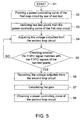
- FIG. 5 shows a flowchart of a method for controlling laser power of an optical disk drive according to the preferred embodiment of the invention.
- a reference signal can be respectively inputted to an open-loop control circuit 1 and a closed-loop control circuit 2 to generate a voltage (or a current).
- the generated voltage is outputted to a pick-up head 3 of the optical disc drive.
- an internal power signal such as Front Photo Diode Output signal (abbreviated as FPDO signal)
- FPDO signal Front Photo Diode Output signal
- the actually outputted laser power can be detected with a power detection unit 5 .
- the open-loop control circuit 1 and the closed-loop control circuit 2 of the power control system of the optical disc drive of the invention have different circuits and result in a shift in the reference level of respective outputted voltage. However, the open-loop control circuit 1 and the closed-loop control circuit 2 do not have any difference in the circuit after the voltage is outputted.
- the outputted voltage generates an output of laser power, and there is a proportional relationship between the two loop circuits.
- FIG. 3 shows a closed-loop circuit power-controlling curve according to the preferred embodiment of the invention
- FIG. 4 shows an open-loop circuit power-controlling curve according to the preferred embodiment of the invention.
- the conventional optical disc drive needs to have real test on the open-loop circuit and closed-loop circuit to obtain respective power-controlling curve of the two loop circuits.
- the method for controlling the laser power of an optical disk drive of the invention the power-controlling curve of one of the two loop circuits is obtained by real test and the power-controlling curve of the other loop circuit is obtained according to the proportional relationship between the two loop circuits.
- the power-controlling curve of the closed-loop circuit is obtained by real test, and the power-controlling curve of open-loop circuit is obtained from the power-controlling curve of the closed-loop circuit.
- the closed-loop control circuit 2 generates a number of different outputted voltages to the pick-up head 3 to excite the laser diode 4 to output a laser power.
- the actual output of laser power is detected by an external power detection unit 5 , and generates a corresponding FPDO signal in the pick-up head 3 .
- the corresponding relationship between the FPDO signal and the actual output of laser power is obtained.
- the response time of the FPDO signal is much faster than that of the external power detection unit 5 . Therefore, the FPDO signal displaces the output power, and the power-controlling curve C of the closed-loop circuit can be obtained by several test point (as denoted by the marks in FIG. 3 ) by way of linear fitting.
- Test points A and B are selected from the test points of the power-controlling curve C of the closed-loop circuit. As the power-controlling curve C of the closed-loop circuit is closer to be linear in the low internal power signal area, the test point is preferably selected from the area closer to the low internal power signal.
- the test points A and B output the voltages V 1 and V 2 and correspondingly generate the internal power signals FPDO 1 and FPDO 2 . As indicated in FIG. 4 , in the open-loop control circuit 1 , the outputted voltage is adjusted and transmitted to the pick-up head 3 , and a relative FPDO signal is figured out from an unknown corresponding relationship curve LE to match with the known internal power signals FPDO 1 and FPDO 2 of the test points A and B.
- the voltage outputted from the open-loop control circuit 1 is multiplied by the gain G, and the actual output power is obtained from the power-controlling curve C of the closed-loop circuit.
- the gained power-controlling curve C of the closed-loop circuit obtained by multiplying the power-controlling curve C of the closed-loop circuit by the gain G is used as the power-controlling curve of open-loop control circuit 1 without doing real test, the power-controlling curve of open-loop circuit and the closed-loop circuit can thus be quickly obtained.
- closed-loop control circuit is the first loop circuit
- the open-loop control circuit is the second loop circuit.
- the method of adjusting the power-controlling curve of the first loop circuit obtained by real test so as to quickly form the power-controlling curve of the second loop circuit are disclosed below. Firstly, the method begins at step S 1 . Next, the method proceeds to step S 2 , the outputted voltage is tested by the first loop control circuit in a real test to obtain a corresponding internal power signal and form a power-controlling curve of the first loop circuit.
- step S 3 two test points are respectively selected from a high internal power signal and a low internal power signal of the power-controlling curve of the first loop circuit.
- step S 4 the voltage outputted from the second loop control circuit is adjusted by aiming at achieving the internal power signal of the two selected test points.
- step S 5 whether the internal power signal generated by the voltage outputted from the second loop control circuit matches with the internal power signal of the two test points is checked. If the generated internal power signal does not match with the internal power signal of the two test points, the method returns to step S 4 and continues to adjust the outputted voltage.
- step S 6 the voltage outputted from the second loop control circuit is recorded. Then, the method proceeds to step S 7 , the gain of the voltage change of the open-loop control circuit compared to the voltage change of the two real test points is calculated under the same change of the internal power signal. Lastly, the method proceeds to step S 8 , the gained power-controlling curve of the first loop circuit is used as the power-controlling curve of the second loop control circuit so as to obtain the power-controlling curve of the second loop control circuit.
- the power-controlling curve of one of the two loop circuits obtained in a real test is used to form the power-controlling curve of the other loop circuit.
- the voltage outputted from the other loop circuit is adjusted to achieve the same internal power signal.
- the change in the outputted voltage is obtained.
- the gain on the outputted voltage between two loop circuits is calculated.
- the voltage outputted from the other loop circuit after suitable gain adjustment, obtains an output power from the power-controlling curve of the loop circuit obtained in real test, such that the power-controlling curve of the other loop circuit is formed from the gained power-controlling curve of the loop circuit obtained in real test.
- the method of the invention saves the required time for testing the power-controlling curve of the other loop circuit.
- the power-controlling curve of the other loop circuit can be quickly formed by use of original internal power signal (FPDO signal) and can do without the signal feedbacked via the external power detection unit.
Landscapes
- Physics & Mathematics (AREA)
- Optics & Photonics (AREA)
- Optical Recording Or Reproduction (AREA)
- Optical Head (AREA)
Abstract
Description
[(V2−V1)/(FPDO2−FPDO1)]×G=[(VE2−VE1)/(FPDO2−FPDO1)]
Claims (7)
[(V2−V1)/(FPDO2−FPDO1)]×G=[(VE2−VE1)/(FPDO2−FPDO1)]
Applications Claiming Priority (3)
| Application Number | Priority Date | Filing Date | Title |
|---|---|---|---|
| TW096144695A TW200923932A (en) | 2007-11-23 | 2007-11-23 | Method for contolling power of optical disk drive |
| TW96144695A | 2007-11-23 | ||
| TW96144695 | 2007-11-23 |
Publications (2)
| Publication Number | Publication Date |
|---|---|
| US20090135865A1 US20090135865A1 (en) | 2009-05-28 |
| US7965746B2 true US7965746B2 (en) | 2011-06-21 |
Family
ID=40669655
Family Applications (1)
| Application Number | Title | Priority Date | Filing Date |
|---|---|---|---|
| US12/289,124 Expired - Fee Related US7965746B2 (en) | 2007-11-23 | 2008-10-21 | Method for controlling power of an optical disk drive |
Country Status (2)
| Country | Link |
|---|---|
| US (1) | US7965746B2 (en) |
| TW (1) | TW200923932A (en) |
Families Citing this family (1)
| Publication number | Priority date | Publication date | Assignee | Title |
|---|---|---|---|---|
| JP5207559B2 (en) * | 2010-12-15 | 2013-06-12 | パナソニック株式会社 | Optical information recording / reproducing apparatus |
-
2007
- 2007-11-23 TW TW096144695A patent/TW200923932A/en unknown
-
2008
- 2008-10-21 US US12/289,124 patent/US7965746B2/en not_active Expired - Fee Related
Also Published As
| Publication number | Publication date |
|---|---|
| TW200923932A (en) | 2009-06-01 |
| US20090135865A1 (en) | 2009-05-28 |
Similar Documents
| Publication | Publication Date | Title |
|---|---|---|
| US7738333B2 (en) | Optical disk drive for writing a re-writable optical disk and method thereof | |
| US7313068B2 (en) | Apparatus and method for automatic power control | |
| US7965746B2 (en) | Method for controlling power of an optical disk drive | |
| US7420906B2 (en) | Automatic power calibration apparatus for optical recording device and automatic power calibration method therefor | |
| US7940821B2 (en) | Temperature compensating method of laser power in optical disk storage apparatus | |
| US6049513A (en) | Method and apparatus for adjusting a focus bias in an optical disc player | |
| US8004942B1 (en) | Method and apparatus for reading | |
| US20070058502A1 (en) | Servo system and related method of adjusting the magnitude of detecting signals outputted from a pick-up head before utilizing the detecting signals to generate servo signals | |
| KR100653492B1 (en) | Laser power setting method of optical disk device | |
| US6865143B2 (en) | Optical device including a calibrating unit for calibrating a level adjusting unit | |
| US20050265205A1 (en) | Method for real-time adjustment of servo gain in an optical recording system according to reflected recording light beam | |
| CN100442366C (en) | Temperature compensating method of laser power in optical disk storage apparatus | |
| JP2002334440A (en) | Optical recording / reproducing device | |
| CN101471097A (en) | Power control method for optical disk drive | |
| US6549501B2 (en) | Method for adjusting reflective light disturbance optical disk drive | |
| EP1777704A1 (en) | Disk device, and signal producing method | |
| US8320223B2 (en) | Optical storage apparatus and method for eliminating write power transient thereof | |
| US7663987B2 (en) | Method and system for calibrating recording track offset of optical storage device | |
| JP3183975B2 (en) | Tracking control circuit | |
| US20050122859A1 (en) | Method and apparatus of mirror signal auto-calibration for optical disk drive | |
| KR20050057077A (en) | Apparatus for sensing defect of optical disk | |
| JP2002260252A (en) | Tracking control method for optical disk apparatus | |
| US20100188943A1 (en) | Optical storage apparatus and method for automatically adjusting loop gain thereof | |
| JP2007200444A (en) | Optical output adjusting device and optical output adjusting method for optical pickup, and optical pickup adjusted by the method | |
| JP2003187439A (en) | Light emission power adjusting device, optical disk recording / reproducing device, and light emission power adjusting method thereof |
Legal Events
| Date | Code | Title | Description |
|---|---|---|---|
| AS | Assignment |
Owner name: QUANTA STORAGE INC., TAIWAN Free format text: ASSIGNMENT OF ASSIGNORS INTEREST;ASSIGNORS:HSU, CHIA-HSING;HSIAO, YI-LONG;REEL/FRAME:021771/0552 Effective date: 20081014 |
|
| REMI | Maintenance fee reminder mailed | ||
| LAPS | Lapse for failure to pay maintenance fees | ||
| LAPS | Lapse for failure to pay maintenance fees |
Free format text: PATENT EXPIRED FOR FAILURE TO PAY MAINTENANCE FEES (ORIGINAL EVENT CODE: EXP.) |
|
| STCH | Information on status: patent discontinuation |
Free format text: PATENT EXPIRED DUE TO NONPAYMENT OF MAINTENANCE FEES UNDER 37 CFR 1.362 |
|
| FP | Lapsed due to failure to pay maintenance fee |
Effective date: 20150621 |
|
| STCH | Information on status: patent discontinuation |
Free format text: PATENT EXPIRED DUE TO NONPAYMENT OF MAINTENANCE FEES UNDER 37 CFR 1.362 |