US7947202B2 - Polymer-nanoparticle compositions and methods of making and using same - Google Patents
Polymer-nanoparticle compositions and methods of making and using same Download PDFInfo
- Publication number
- US7947202B2 US7947202B2 US12/194,848 US19484808A US7947202B2 US 7947202 B2 US7947202 B2 US 7947202B2 US 19484808 A US19484808 A US 19484808A US 7947202 B2 US7947202 B2 US 7947202B2
- Authority
- US
- United States
- Prior art keywords
- polymer
- nanoparticle
- metal
- copolymer
- film
- Prior art date
- Legal status (The legal status is an assumption and is not a legal conclusion. Google has not performed a legal analysis and makes no representation as to the accuracy of the status listed.)
- Expired - Fee Related, expires
Links
- 0 *C.C1=CCC(C2=CC=C(C3=CC=C4OC5(N=CC4=C3)N=CC3=C/C(C4=CC=C(C6=CC=CC6)C4)=C\C=C\3O5)C2)=C1.[1*]C.[2*]C.[3*]C.[5*]C.[6*]C Chemical compound *C.C1=CCC(C2=CC=C(C3=CC=C4OC5(N=CC4=C3)N=CC3=C/C(C4=CC=C(C6=CC=CC6)C4)=C\C=C\3O5)C2)=C1.[1*]C.[2*]C.[3*]C.[5*]C.[6*]C 0.000 description 6
- XKMRRTOUMJRJIA-UHFFFAOYSA-N N.N Chemical compound N.N XKMRRTOUMJRJIA-UHFFFAOYSA-N 0.000 description 6
- NAJXRAGXYKOBSX-PZTKHUHLSA-L C.C.C.C.C.CC1=CC=C(C2=CC=C(C3=CC=C(C4=CC=C(C5=CC=C6O[Pd@@]78O/C9=C\C=C(C%10=CC=C(C%11=CC=C(C)S%11)S%10)/C=C9/C=N\7CC(C)(C)CN8=CC6=C5)S4)S3)S2)S1 Chemical compound C.C.C.C.C.CC1=CC=C(C2=CC=C(C3=CC=C(C4=CC=C(C5=CC=C6O[Pd@@]78O/C9=C\C=C(C%10=CC=C(C%11=CC=C(C)S%11)S%10)/C=C9/C=N\7CC(C)(C)CN8=CC6=C5)S4)S3)S2)S1 NAJXRAGXYKOBSX-PZTKHUHLSA-L 0.000 description 1
- BJQDQCVTFWJAKE-UHFFFAOYSA-L C1=CSC(C2=CC=C(C3=CC=C4O[Cd]5(N=CC6=C/C(C7=CC=C(C8=CC=CS8)S7)=C/C=C\6O5)/N=C\C4=C3)S2)=C1 Chemical compound C1=CSC(C2=CC=C(C3=CC=C4O[Cd]5(N=CC6=C/C(C7=CC=C(C8=CC=CS8)S7)=C/C=C\6O5)/N=C\C4=C3)S2)=C1 BJQDQCVTFWJAKE-UHFFFAOYSA-L 0.000 description 1
- FGEOIYQEYAYOTQ-ULQPCQOVSA-H C1=CSC(C2=CC=C(C3=CC=C4O[Cd]56OC7=CC=C(C8=CC=C(C9=CC=CS9)S8)C=C7C=N5C5=C(C=CC=C5)N6=CC4=C3)S2)=C1.C1=CSC(C2=CC=C(C3=CC=C4O[Cd]56OC7=CC=C(C8=CC=C(C9=CC=CS9)S8)C=C7C=N5CCOCCOCCN6=CC4=C3)S2)=C1.CC1(C)CN2=CC3=CC(C4=CC=C(C5=CC=CS5)S4)=CC=C3O[Cd]23OC2=CC=C(C4=CC=C(C5=CC=CS5)S4)C=C2C=N3C1 Chemical compound C1=CSC(C2=CC=C(C3=CC=C4O[Cd]56OC7=CC=C(C8=CC=C(C9=CC=CS9)S8)C=C7C=N5C5=C(C=CC=C5)N6=CC4=C3)S2)=C1.C1=CSC(C2=CC=C(C3=CC=C4O[Cd]56OC7=CC=C(C8=CC=C(C9=CC=CS9)S8)C=C7C=N5CCOCCOCCN6=CC4=C3)S2)=C1.CC1(C)CN2=CC3=CC(C4=CC=C(C5=CC=CS5)S4)=CC=C3O[Cd]23OC2=CC=C(C4=CC=C(C5=CC=CS5)S4)C=C2C=N3C1 FGEOIYQEYAYOTQ-ULQPCQOVSA-H 0.000 description 1
Images


Classifications
-
- H—ELECTRICITY
- H01—ELECTRIC ELEMENTS
- H01B—CABLES; CONDUCTORS; INSULATORS; SELECTION OF MATERIALS FOR THEIR CONDUCTIVE, INSULATING OR DIELECTRIC PROPERTIES
- H01B1/00—Conductors or conductive bodies characterised by the conductive materials; Selection of materials as conductors
- H01B1/06—Conductors or conductive bodies characterised by the conductive materials; Selection of materials as conductors mainly consisting of other non-metallic substances
- H01B1/12—Conductors or conductive bodies characterised by the conductive materials; Selection of materials as conductors mainly consisting of other non-metallic substances organic substances
- H01B1/124—Intrinsically conductive polymers
- H01B1/127—Intrinsically conductive polymers comprising five-membered aromatic rings in the main chain, e.g. polypyrroles, polythiophenes
-
- B—PERFORMING OPERATIONS; TRANSPORTING
- B82—NANOTECHNOLOGY
- B82Y—SPECIFIC USES OR APPLICATIONS OF NANOSTRUCTURES; MEASUREMENT OR ANALYSIS OF NANOSTRUCTURES; MANUFACTURE OR TREATMENT OF NANOSTRUCTURES
- B82Y30/00—Nanotechnology for materials or surface science, e.g. nanocomposites
-
- C—CHEMISTRY; METALLURGY
- C07—ORGANIC CHEMISTRY
- C07D—HETEROCYCLIC COMPOUNDS
- C07D409/00—Heterocyclic compounds containing two or more hetero rings, at least one ring having sulfur atoms as the only ring hetero atoms
- C07D409/14—Heterocyclic compounds containing two or more hetero rings, at least one ring having sulfur atoms as the only ring hetero atoms containing three or more hetero rings
-
- C—CHEMISTRY; METALLURGY
- C08—ORGANIC MACROMOLECULAR COMPOUNDS; THEIR PREPARATION OR CHEMICAL WORKING-UP; COMPOSITIONS BASED THEREON
- C08G—MACROMOLECULAR COMPOUNDS OBTAINED OTHERWISE THAN BY REACTIONS ONLY INVOLVING UNSATURATED CARBON-TO-CARBON BONDS
- C08G61/00—Macromolecular compounds obtained by reactions forming a carbon-to-carbon link in the main chain of the macromolecule
- C08G61/12—Macromolecular compounds containing atoms other than carbon in the main chain of the macromolecule
- C08G61/122—Macromolecular compounds containing atoms other than carbon in the main chain of the macromolecule derived from five- or six-membered heterocyclic compounds, other than imides
- C08G61/123—Macromolecular compounds containing atoms other than carbon in the main chain of the macromolecule derived from five- or six-membered heterocyclic compounds, other than imides derived from five-membered heterocyclic compounds
- C08G61/126—Macromolecular compounds containing atoms other than carbon in the main chain of the macromolecule derived from five- or six-membered heterocyclic compounds, other than imides derived from five-membered heterocyclic compounds with a five-membered ring containing one sulfur atom in the ring
-
- H—ELECTRICITY
- H01—ELECTRIC ELEMENTS
- H01B—CABLES; CONDUCTORS; INSULATORS; SELECTION OF MATERIALS FOR THEIR CONDUCTIVE, INSULATING OR DIELECTRIC PROPERTIES
- H01B1/00—Conductors or conductive bodies characterised by the conductive materials; Selection of materials as conductors
- H01B1/02—Conductors or conductive bodies characterised by the conductive materials; Selection of materials as conductors mainly consisting of metals or alloys
-
- H—ELECTRICITY
- H10—SEMICONDUCTOR DEVICES; ELECTRIC SOLID-STATE DEVICES NOT OTHERWISE PROVIDED FOR
- H10K—ORGANIC ELECTRIC SOLID-STATE DEVICES
- H10K30/00—Organic devices sensitive to infrared radiation, light, electromagnetic radiation of shorter wavelength or corpuscular radiation
- H10K30/30—Organic devices sensitive to infrared radiation, light, electromagnetic radiation of shorter wavelength or corpuscular radiation comprising bulk heterojunctions, e.g. interpenetrating networks of donor and acceptor material domains
- H10K30/35—Organic devices sensitive to infrared radiation, light, electromagnetic radiation of shorter wavelength or corpuscular radiation comprising bulk heterojunctions, e.g. interpenetrating networks of donor and acceptor material domains comprising inorganic nanostructures, e.g. CdSe nanoparticles
-
- H—ELECTRICITY
- H10—SEMICONDUCTOR DEVICES; ELECTRIC SOLID-STATE DEVICES NOT OTHERWISE PROVIDED FOR
- H10K—ORGANIC ELECTRIC SOLID-STATE DEVICES
- H10K85/00—Organic materials used in the body or electrodes of devices covered by this subclass
- H10K85/30—Coordination compounds
-
- H—ELECTRICITY
- H10—SEMICONDUCTOR DEVICES; ELECTRIC SOLID-STATE DEVICES NOT OTHERWISE PROVIDED FOR
- H10K—ORGANIC ELECTRIC SOLID-STATE DEVICES
- H10K85/00—Organic materials used in the body or electrodes of devices covered by this subclass
- H10K85/60—Organic compounds having low molecular weight
- H10K85/649—Aromatic compounds comprising a hetero atom
- H10K85/655—Aromatic compounds comprising a hetero atom comprising only sulfur as heteroatom
-
- C—CHEMISTRY; METALLURGY
- C08—ORGANIC MACROMOLECULAR COMPOUNDS; THEIR PREPARATION OR CHEMICAL WORKING-UP; COMPOSITIONS BASED THEREON
- C08G—MACROMOLECULAR COMPOUNDS OBTAINED OTHERWISE THAN BY REACTIONS ONLY INVOLVING UNSATURATED CARBON-TO-CARBON BONDS
- C08G2261/00—Macromolecular compounds obtained by reactions forming a carbon-to-carbon link in the main chain of the macromolecule
- C08G2261/10—Definition of the polymer structure
- C08G2261/12—Copolymers
- C08G2261/124—Copolymers alternating
-
- C—CHEMISTRY; METALLURGY
- C08—ORGANIC MACROMOLECULAR COMPOUNDS; THEIR PREPARATION OR CHEMICAL WORKING-UP; COMPOSITIONS BASED THEREON
- C08G—MACROMOLECULAR COMPOUNDS OBTAINED OTHERWISE THAN BY REACTIONS ONLY INVOLVING UNSATURATED CARBON-TO-CARBON BONDS
- C08G2261/00—Macromolecular compounds obtained by reactions forming a carbon-to-carbon link in the main chain of the macromolecule
- C08G2261/10—Definition of the polymer structure
- C08G2261/19—Definition of the polymer structure partially conjugated
-
- C—CHEMISTRY; METALLURGY
- C08—ORGANIC MACROMOLECULAR COMPOUNDS; THEIR PREPARATION OR CHEMICAL WORKING-UP; COMPOSITIONS BASED THEREON
- C08G—MACROMOLECULAR COMPOUNDS OBTAINED OTHERWISE THAN BY REACTIONS ONLY INVOLVING UNSATURATED CARBON-TO-CARBON BONDS
- C08G2261/00—Macromolecular compounds obtained by reactions forming a carbon-to-carbon link in the main chain of the macromolecule
- C08G2261/30—Monomer units or repeat units incorporating structural elements in the main chain
- C08G2261/31—Monomer units or repeat units incorporating structural elements in the main chain incorporating aromatic structural elements in the main chain
- C08G2261/312—Non-condensed aromatic systems, e.g. benzene
-
- C—CHEMISTRY; METALLURGY
- C08—ORGANIC MACROMOLECULAR COMPOUNDS; THEIR PREPARATION OR CHEMICAL WORKING-UP; COMPOSITIONS BASED THEREON
- C08G—MACROMOLECULAR COMPOUNDS OBTAINED OTHERWISE THAN BY REACTIONS ONLY INVOLVING UNSATURATED CARBON-TO-CARBON BONDS
- C08G2261/00—Macromolecular compounds obtained by reactions forming a carbon-to-carbon link in the main chain of the macromolecule
- C08G2261/30—Monomer units or repeat units incorporating structural elements in the main chain
- C08G2261/32—Monomer units or repeat units incorporating structural elements in the main chain incorporating heteroaromatic structural elements in the main chain
- C08G2261/322—Monomer units or repeat units incorporating structural elements in the main chain incorporating heteroaromatic structural elements in the main chain non-condensed
- C08G2261/3223—Monomer units or repeat units incorporating structural elements in the main chain incorporating heteroaromatic structural elements in the main chain non-condensed containing one or more sulfur atoms as the only heteroatom, e.g. thiophene
-
- C—CHEMISTRY; METALLURGY
- C08—ORGANIC MACROMOLECULAR COMPOUNDS; THEIR PREPARATION OR CHEMICAL WORKING-UP; COMPOSITIONS BASED THEREON
- C08G—MACROMOLECULAR COMPOUNDS OBTAINED OTHERWISE THAN BY REACTIONS ONLY INVOLVING UNSATURATED CARBON-TO-CARBON BONDS
- C08G2261/00—Macromolecular compounds obtained by reactions forming a carbon-to-carbon link in the main chain of the macromolecule
- C08G2261/30—Monomer units or repeat units incorporating structural elements in the main chain
- C08G2261/36—Oligomers, i.e. comprising up to 10 repeat units
-
- C—CHEMISTRY; METALLURGY
- C08—ORGANIC MACROMOLECULAR COMPOUNDS; THEIR PREPARATION OR CHEMICAL WORKING-UP; COMPOSITIONS BASED THEREON
- C08G—MACROMOLECULAR COMPOUNDS OBTAINED OTHERWISE THAN BY REACTIONS ONLY INVOLVING UNSATURATED CARBON-TO-CARBON BONDS
- C08G2261/00—Macromolecular compounds obtained by reactions forming a carbon-to-carbon link in the main chain of the macromolecule
- C08G2261/30—Monomer units or repeat units incorporating structural elements in the main chain
- C08G2261/37—Metal complexes
-
- C—CHEMISTRY; METALLURGY
- C08—ORGANIC MACROMOLECULAR COMPOUNDS; THEIR PREPARATION OR CHEMICAL WORKING-UP; COMPOSITIONS BASED THEREON
- C08G—MACROMOLECULAR COMPOUNDS OBTAINED OTHERWISE THAN BY REACTIONS ONLY INVOLVING UNSATURATED CARBON-TO-CARBON BONDS
- C08G2261/00—Macromolecular compounds obtained by reactions forming a carbon-to-carbon link in the main chain of the macromolecule
- C08G2261/40—Polymerisation processes
- C08G2261/44—Electrochemical polymerisation, i.e. oxidative or reductive coupling
-
- C—CHEMISTRY; METALLURGY
- C08—ORGANIC MACROMOLECULAR COMPOUNDS; THEIR PREPARATION OR CHEMICAL WORKING-UP; COMPOSITIONS BASED THEREON
- C08L—COMPOSITIONS OF MACROMOLECULAR COMPOUNDS
- C08L65/00—Compositions of macromolecular compounds obtained by reactions forming a carbon-to-carbon link in the main chain; Compositions of derivatives of such polymers
-
- H—ELECTRICITY
- H10—SEMICONDUCTOR DEVICES; ELECTRIC SOLID-STATE DEVICES NOT OTHERWISE PROVIDED FOR
- H10K—ORGANIC ELECTRIC SOLID-STATE DEVICES
- H10K30/00—Organic devices sensitive to infrared radiation, light, electromagnetic radiation of shorter wavelength or corpuscular radiation
- H10K30/50—Photovoltaic [PV] devices
-
- Y—GENERAL TAGGING OF NEW TECHNOLOGICAL DEVELOPMENTS; GENERAL TAGGING OF CROSS-SECTIONAL TECHNOLOGIES SPANNING OVER SEVERAL SECTIONS OF THE IPC; TECHNICAL SUBJECTS COVERED BY FORMER USPC CROSS-REFERENCE ART COLLECTIONS [XRACs] AND DIGESTS
- Y02—TECHNOLOGIES OR APPLICATIONS FOR MITIGATION OR ADAPTATION AGAINST CLIMATE CHANGE
- Y02E—REDUCTION OF GREENHOUSE GAS [GHG] EMISSIONS, RELATED TO ENERGY GENERATION, TRANSMISSION OR DISTRIBUTION
- Y02E10/00—Energy generation through renewable energy sources
- Y02E10/50—Photovoltaic [PV] energy
- Y02E10/549—Organic PV cells
Definitions
- Electrically conducting polymers are well known for their use in electrical and optical devices due to their ability to transport charge.
- One drawback to these materials is that electron transport in conducting polymers is much slower than hole transport.
- preformed nanoparticles have been directly blended with conducting polymers. In theory, such a blend should enable the separation of the exciton at the interface between the two materials, such that the polymer is the hole transporter while the nanoparticles are the electron transporters.
- the invention in various aspects, relates to materials for use in light-emitting devices, energy conversion devices, devices produced therewith, and methods for making same.
- the present application provides a polymer-nanoparticle compositions comprising: a film comprising an at least partially electrically conductive oligomer, polymer, or copolymer; and at least one nanoparticle at least partially disposed therein; wherein the at least partially electrically conductive oligomer, polymer, or copolymer is in electrical communication with the nanoparticle.
- the nanoparticle comprises a semiconductor material.
- the nanoparticle comprises a metal, such as, for example, a transition metal, a platinum group metal, or a combination thereof.
- the present application provides methods for producing polymer nanoparticle compositions comprising: providing a film comprising an at least partially electrically conductive oligomer, polymer, or copolymer comprising a plurality of metal complex residues having at least one metal center therein; and growing at least one nanoparticle from the at least one metal center; thereby producing the polymer-nanoparticle composition.
- semiconducting devices comprising: a polymer nanoparticle composition comprising at least one nanoparticle having one or more layers of at least one metal; an at least partially electrically conductive oligomer, polymer, or copolymer; wherein the at least partially electrically conductive oligomer, polymer, or copolymer and the nanoparticle are in electrical communication with each other; and wherein the at least one nanoparticle is produced from at least one metal center in a metal complex residue in the at least partially electrically conductive oligomer, polymer, or copolymer.
- each Y 1 , Y 2 , Y 3 , and Y 4 is independently selected from O, S, and NH; wherein M is a metal; wherein each R 1 , R 2 , R 3 , and R 4 independently comprises 3 substituents independently selected from hydrogen and optionally substituted organic residue comprising from 1 to 12 carbons; wherein each R 5 and R 6 independently comprises 3 substituents independently selected from hydrogen and optionally substituted organic residue comprising from 1 to 12 carbons; wherein the general structural residue
- the metal represents a ligand selected from optionally substituted heteroalkyl, optionally substituted heterocycloalkyl, and optionally substituted heteroaryl; or an oligomer, polymer, or nanoparticle produced therefrom.
- the metal comprises Cd, Pb, Ga, or a combination thereof.
- the metal comprises a transition metal, such as for example, Co; an inert metal, such as, for example, gold; a platinum group metal, such as, for example, platinum, palladium, ruthenium; or a combination thereof.
- oligomers, polymers, or copolymers comprising a residue represented by a formula:
- n is an integer from 1 to 100,000; wherein each Y 1 , Y 2 , Y 3 , and Y 4 is independently selected from O, S, and NH; wherein M is a metal; wherein each R 1 and R 4 independently comprises 2 substituents independently selected from hydrogen and optionally substituted organic residue comprising from 1 to 12 carbons; wherein each R 2 and R 3 independently comprises 3 substituents independently selected from hydrogen and optionally substituted organic residue comprising from 1 to 12 carbons; wherein each R 5 and R 6 independently comprises from 1 to 3 substituents independently selected from hydrogen and optionally substituted organic residue comprising from 1 to 12 carbons; wherein the general structural residue
- the metal represents a ligand selected from optionally substituted heteroalkyl, optionally substituted heterocycloalkyl, and optionally substituted heteroaryl; or a nanoparticle produced therefrom.
- the metal comprises a transition metal, such as for example, Co; an inert metal, such as, for example, gold; a platinum group metal, such as, for example, platinum, palladium, ruthenium; or a combination thereof.
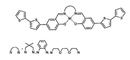
- FIG. 1 is an illustration of the chemical structure of one particular, non-limiting embodiment of a class of monomers made in accordance with the teachings herein which have a metal center and a conducting polymer precursor;
- FIG. 2 is an illustration of a synthetic route which may be utilized to synthesize the monomers of FIG. 1 ;
- FIG. 3 is an illustration of the crystal structure of one particular species in the class of monomers (a tri-nuclear monomer) depicted in FIG. 1 ;
- FIG. 4 is an illustration of the equilibrium existing between a tri-nuclear species and a mono-nuclear species in a cadmium monomer made in accordance with the teachings herein, wherein the center cadmium in the compound is held in place by two residual acetates from the cadmium acetate starting material;
- FIG. 5 depicts the UV visible absorption spectra of the polymer of FIG. 7 , taken at the points noted in the cyclic voltammogram of FIG. 6 ;
- FIG. 6 is a cyclic voltammogram of the polymer shown in FIG. 7 ;
- FIG. 7 depicts the UV visible absorption spectra of the copolymer of FIG. 31 , taken at the points noted in the cyclic voltammogram of FIG. 8 ;
- FIG. 8 is a cyclic voltammogram of the polymer shown in FIG. 31 ;
- FIG. 9 is a graph of the size distribution of nanoparticles formed after two cycles of the process depicted in FIG. 22 ;
- FIG. 10 is a graph of the size distribution of nanoparticles formed after four cycles of the process depicted in FIG. 22 ;
- FIG. 11 is a cyclic voltammogram illustrating the electrodeposition of polymeric films made from the monomer of FIG. 1 ;
- FIG. 12 is an illustration of the electrochemically induced polymerization of one particular species of the class of monomers depicted in FIG. 1 ;
- FIG. 13 is a graph summarizing the data of FIG. 11 ;
- FIG. 14 is a graph depicting the characterization of a film formed by the polymerization shown in FIG. 12 , in which the film on the electrode is characterized by running it through a cyclical voltammogram at different scan rates ranging from a slow scan rate (10 mV/s) to a fast scan rate (500 mV/s);
- FIG. 15 is a graph summarizing the data of FIG. 14 ;
- FIG. 16 is a cyclic voltammogram illustrating the electrodeposition of a copolymer formed by the electrochemical process depicted in FIG. 18 ;
- FIG. 17 is a graph summarizing the data of FIG. 16 ;
- FIG. 18 is an illustration of the electrochemically induced copolymerization of bithiophene and a particular species of the class of monomers depicted in FIG. 1 ;
- FIG. 19 is a graph depicting the characterization of a film formed by the polymerization shown in FIG. 18 , in which the film on the electrode is characterized by running it through a cyclical voltammogram at different scan rates ranging from a slow scan rate (10 mV/s) to a fast scan rate (500 mV/s);
- FIG. 20 is an illustration of the chemical structure of the polymer formed by the electrochemical process of FIG. 12 ;
- FIG. 21 is an illustration of the chemical structure of the copolymer formed by the electrochemical process depicted in FIG. 18 ;
- FIG. 22 is an illustration of the layer by layer growth of cadmium sulfide nanoparticles on the metal centers of the polymer of FIG. 20 ;
- FIG. 23 is a transmission electron micrograph of a film of the polymer after the growth of nanoparticles shown in FIG. 9 ;
- FIG. 24 is a micrograph of a film of the polymer after the growth of nanoparticles shown in FIG. 10 ;
- FIG. 25 is a graph of the size distribution of nanoparticles formed after two cycles of the process depicted in FIG. 22 , but using the bithiophene copolymer depicted in FIG. 21 ;
- FIG. 26 is a micrograph of a film of the polymer after the growth of nanoparticles shown in FIG. 25 ;
- FIG. 27 is a graph of the size distribution of nanoparticles formed after four cycles of the process depicted in FIG. 22 , but using the bithiophene copolymer depicted in FIG. 21 ;
- FIG. 28 is a micrograph of a film of the polymer after the growth of nanoparticles shown in FIG. 27 ;
- FIG. 29 is a series of XPS spectra on the polymer of FIG. 20 (the undiluted cadmium-containing monomer) and copolymers of the type shown in FIG. 31 made with successively greater ratios of bithiophene to the cadmium monomer.
- FIG. 30 is a graph summarizing the data of FIG. 19 ;
- a metal complex residue As used in the specification and the appended claims, the singular forms “a,” “an” and “the” include plural referents unless the context clearly dictates otherwise. Thus, for example, reference to “a metal complex residue,” “a polymer,” or “a nanoparticle” includes mixtures of two or more such metal complex residues, polymers, or nanoparticles, and the like.
- Ranges can be expressed herein as from “about” one particular value, and/or to “about” another particular value. When such a range is expressed, another aspect includes from the one particular value and/or to the other particular value. Similarly, when values are expressed as approximations, by use of the antecedent “about,” it will be understood that the particular value forms another aspect. It will be further understood that the endpoints of each of the ranges are significant both in relation to the other endpoint, and independently of the other endpoint. It is also understood that there are a number of values disclosed herein, and that each value is also herein disclosed as “about” that particular value in addition to the value itself. For example, if the value “10” is disclosed, then “about 10” is also disclosed. It is also understood that each unit between two particular units are also disclosed. For example, if 10 and 15 are disclosed, then 11, 12, 13, and 14 are also disclosed.
- the terms “optional” or “optionally” means that the subsequently described event or circumstance can or can not occur, and that the description includes instances where said event or circumstance occurs and instances where it does not.
- compositions of the invention Disclosed are the components to be used to prepare the compositions of the invention as well as the compositions themselves to be used within the methods disclosed herein.
- these and other materials are disclosed herein, and it is understood that when combinations, subsets, interactions, groups, etc. of these materials are disclosed that while specific reference of each various individual and collective combinations and permutation of these compounds can not be explicitly disclosed, each is specifically contemplated and described herein. For example, if a particular compound is disclosed and discussed and a number of modifications that can be made to a number of molecules including the compounds are discussed, specifically contemplated is each and every combination and permutation of the compound and the modifications that are possible unless specifically indicated to the contrary.
- compositions disclosed herein have certain functions. Disclosed herein are certain structural requirements for performing the disclosed functions, and it is understood that there are a variety of structures that can perform the same function that are related to the disclosed structures, and that these structures will typically achieve the same result.
- a residue of a chemical species refers to the moiety that is the resulting product of the chemical species in a particular reaction scheme or subsequent formulation or chemical product, regardless of whether the moiety is actually obtained from the chemical species.
- a bithiopene residue in a polythiophene refers to one or more bithiophene units in the polythiophene, regardless of whether bithiophene was used to prepare the polythiophene.
- the term “substituted” is contemplated to include all permissible substituents of organic compounds.
- the permissible substituents include acyclic and cyclic, branched and unbranched, carbocyclic and heterocyclic, and aromatic and nonaromatic substituents of organic compounds.
- Illustrative substituents include, for example, those described below.
- the permissible substituents can be one or more and the same or different for appropriate organic compounds.
- the heteroatoms, such as nitrogen can have hydrogen substituents and/or any permissible substituents of organic compounds described herein which satisfy the valences of the heteroatoms.
- substitution or “substituted with” include the implicit proviso that such substitution is in accordance with permitted valence of the substituted atom and the substituent, and that the substitution results in a stable compound, e.g., a compound that does not spontaneously undergo transformation such as by rearrangement, cyclization, elimination, etc.
- substitution or “substituted with” include the implicit proviso that such substitution is in accordance with permitted valence of the substituted atom and the substituent, and that the substitution results in a stable compound, e.g., a compound that does not spontaneously undergo transformation such as by rearrangement, cyclization, elimination, etc.
- optionally substituted means that the compound, atom, or residue can or cannot be substituted, as defined herein.
- a 1 ,” “A 2 ,” “A 3 ,” and “A 4 ” are used herein as generic symbols to represent various specific substituents. These symbols can be any substituent, not limited to those disclosed herein, and when they are defined to be certain substituents in one instance, they can, in another instance, be defined as some other substituents.
- alkyl as used herein is a branched or unbranched saturated hydrocarbon group of 1 to 24 carbon atoms, 1 to 20 carbons, 1 to 18 carbons, 1 to 16 carbons, 1 to 14 carbons, 1 to 10 carbons, 1 to 8 carbons, 1 to 6 carbons, 1 to 4 carbons, 1 to 3 carbons, or 1 to 2 carbons, such as methyl, ethyl, n-propyl, isopropyl, n-butyl, isobutyl, s-butyl, t-butyl, n-pentyl, isopentyl, s-pentyl, neopentyl, hexyl, heptyl, octyl, nonyl, decyl, dodecyl, tetradecyl, hexadecyl, eicosyl, tetracosyl, and the like.
- the alkyl group can also be substituted or unsubstituted.
- the alkyl group can be substituted with one or more groups including, but not limited to, optionally substituted alkyl, cycloalkyl, alkoxy, amino, ether, halide, hydroxy, nitro, silyl, sulfo-oxo, or thiol, as described herein.
- a “lower alkyl” group is an alkyl group containing from one to six (e.g., from one to four) carbon atoms.
- alkyl is generally used to refer to both unsubstituted alkyl groups and substituted alkyl groups; however, substituted alkyl groups are also specifically referred to herein by identifying the specific substituent(s) on the alkyl group.
- halogenated alkyl specifically refers to an alkyl group that is substituted with one or more halide, e.g., fluorine, chlorine, bromine, or iodine.
- alkoxyalkyl specifically refers to an alkyl group that is substituted with one or more alkoxy groups, as described below.
- alkylamino specifically refers to an alkyl group that is substituted with one or more amino groups, as described below, and the like.
- alkyl is used in one instance and a specific term such as “alkylalcohol” is used in another, it is not meant to imply that the term “alkyl” does not also refer to specific terms such as “alkylalcohol” and the like.
- cycloalkyl refers to both unsubstituted and substituted cycloalkyl moieties
- the substituted moieties can, in addition, be specifically identified herein; for example, a particular substituted cycloalkyl can be referred to as, e.g., an “alkylcycloalkyl.”
- a substituted alkoxy can be specifically referred to as, e.g., a “halogenated alkoxy”
- a particular substituted alkenyl can be, e.g., an “alkenylalcohol,” and the like.
- the practice of using a general term, such as “cycloalkyl,” and a specific term, such as “alkylcycloalkyl,” is not meant to imply that the general term does not also include the specific term.
- cycloalkyl as used herein is a non-aromatic carbon-based ring composed of at least three carbon atoms.
- examples of cycloalkyl groups include, but are not limited to, cyclopropyl, cyclobutyl, cyclopentyl, cyclohexyl, norbornyl, and the like.
- heterocycloalkyl is a type of cycloalkyl group as defined above, and is included within the meaning of the term “cycloalkyl,” where at least one of the carbon atoms of the ring is replaced with a heteroatom such as, but not limited to, nitrogen, oxygen, sulfur, or phosphorus.
- the cycloalkyl group and heterocycloalkyl group can be substituted or unsubstituted.
- the cycloalkyl group and heterocycloalkyl group can be substituted with one or more groups including, but not limited to, optionally substituted alkyl, cycloalkyl, alkoxy, amino, ether, halide, hydroxy, nitro, silyl, sulfo-oxo, or thiol as described herein.
- Alkoxy also includes polymers of alkoxy groups as just described; that is, an alkoxy can be a polyether such as —OA 1 -OA 2 or —OA 1 -(OA 2 ) a —OA 3 , where “a” is an integer of from 1 to 200 and A 1 , A 2 , and A 3 are alkyl and/or cycloalkyl groups.
- alkenyl as used herein is a hydrocarbon group of from 2 to 24 carbon atoms with a structural formula containing at least one carbon-carbon double bond.
- Asymmetric structures such as (A 1 A 2 )C ⁇ C(A 3 A 4 ) are intended to include both the E and Z isomers. This can be presumed in structural formulae herein wherein an asymmetric alkene is present, or it can be explicitly indicated by the bond symbol C ⁇ C.
- the alkenyl group can be substituted with one or more groups including, but not limited to, optionally substituted alkyl, cycloalkyl, alkoxy, alkenyl, cycloalkenyl, alkynyl, cycloalkynyl, aryl, heteroaryl, aldehyde, amino, carboxylic acid, ester, ether, halide, hydroxy, ketone, azide, nitro, silyl, sulfo-oxo, or thiol, as described herein.
- cycloalkenyl as used herein is a non-aromatic carbon-based ring composed of at least three carbon atoms and containing at least one carbon-carbon double bound, i.e., C ⁇ C.
- Examples of cycloalkenyl groups include, but are not limited to, cyclopropenyl, cyclobutenyl, cyclopentenyl, cyclopentadienyl, cyclohexenyl, cyclohexadienyl, norbornenyl, and the like.
- heterocycloalkenyl is a type of cycloalkenyl group as defined above, and is included within the meaning of the term “cycloalkenyl,” where at least one of the carbon atoms of the ring is replaced with a heteroatom such as, but not limited to, nitrogen, oxygen, sulfur, or phosphorus.
- the cycloalkenyl group and heterocycloalkenyl group can be substituted or unsubstituted.
- the cycloalkenyl group and heterocycloalkenyl group can be substituted with one or more groups including, but not limited to, optionally substituted alkyl, cycloalkyl, alkoxy, alkenyl, cycloalkenyl, alkynyl, cycloalkynyl, aryl, heteroaryl, aldehyde, amino, carboxylic acid, ester, ether, halide, hydroxy, ketone, azide, nitro, silyl, sulfo-oxo, or thiol as described herein.
- alkynyl as used herein is a hydrocarbon group of 2 to 24 carbon atoms with a structural formula containing at least one carbon-carbon triple bond.
- the alkynyl group can be unsubstituted or substituted with one or more groups including, but not limited to, optionally substituted alkyl, cycloalkyl, alkoxy, alkenyl, cycloalkenyl, alkynyl, cycloalkynyl, aryl, heteroaryl, aldehyde, amino, carboxylic acid, ester, ether, halide, hydroxy, ketone, azide, nitro, silyl, sulfo-oxo, or thiol, as described herein.
- cycloalkynyl as used herein is a non-aromatic carbon-based ring composed of at least seven carbon atoms and containing at least one carbon-carbon triple bound.
- cycloalkynyl groups include, but are not limited to, cycloheptynyl, cyclooctynyl, cyclononynyl, and the like.
- heterocycloalkynyl is a type of cycloalkenyl group as defined above, and is included within the meaning of the term “cycloalkynyl,” where at least one of the carbon atoms of the ring is replaced with a heteroatom such as, but not limited to, nitrogen, oxygen, sulfur, or phosphorus.
- the cycloalkynyl group and heterocycloalkynyl group can be substituted or unsubstituted.
- the cycloalkynyl group and heterocycloalkynyl group can be substituted with one or more groups including, but not limited to, optionally substituted alkyl, cycloalkyl, alkoxy, alkenyl, cycloalkenyl, alkynyl, cycloalkynyl, aryl, heteroaryl, aldehyde, amino, carboxylic acid, ester, ether, halide, hydroxy, ketone, azide, nitro, silyl, sulfo-oxo, or thiol as described herein.
- aryl as used herein is a group that contains any carbon-based aromatic group including, but not limited to, benzene, naphthalene, phenyl, biphenyl, phenoxybenzene, and the like.
- aryl also includes “heteroaryl,” which is defined as a group that contains an aromatic group that has at least one heteroatom incorporated within the ring of the aromatic group. Examples of heteroatoms include, but are not limited to, nitrogen, oxygen, sulfur, and phosphorus.
- non-heteroaryl which is also included in the term “aryl,” defines a group that contains an aromatic group that does not contain a heteroatom. The aryl group can be substituted or unsubstituted.
- the aryl group can be substituted with one or more groups including, but not limited to, optionally substituted alkyl, cycloalkyl, alkoxy, alkenyl, cycloalkenyl, alkynyl, cycloalkynyl, aryl, heteroaryl, aldehyde, amino, carboxylic acid, ester, ether, halide, hydroxy, ketone, azide, nitro, silyl, sulfo-oxo, or thiol as described herein.
- biasing is a specific type of aryl group and is included in the definition of “aryl.”
- Biaryl refers to two aryl groups that are bound together via a fused ring structure, as in naphthalene, or are attached via one or more carbon-carbon bonds, as in biphenyl.
- organic residue defines a carbon containing residue, i.e., a residue comprising at least one carbon atom, and includes but is not limited to the carbon-containing groups, residues, or radicals defined hereinabove.
- Organic residues can contain various heteroatoms, or be bonded to another molecule through a heteroatom, including oxygen, nitrogen, sulfur, phosphorus, or the like. Examples of organic residues include but are not limited alkyl or substituted alkyls, alkoxy or substituted alkoxy, mono or di-substituted amino, amide groups, etc.
- Organic residues can preferably comprise 1 to 18 carbon atoms, 1 to 15, carbon atoms, 1 to 12 carbon atoms, 1 to 8 carbon atoms, 1 to 6 carbon atoms, or 1 to 4 carbon atoms.
- an organic residue can comprise 2 to 18 carbon atoms, 2 to 15, carbon atoms, 2 to 12 carbon atoms, 2 to 8 carbon atoms, 2 to 4 carbon atoms, or 2 to 4 carbon atoms
- a very close synonym of the term “residue” is the term “radical,” which as used in the specification and concluding claims, refers to a fragment, group, or substructure of a molecule described herein, regardless of how the molecule is prepared.
- radical refers to a fragment, group, or substructure of a molecule described herein, regardless of how the molecule is prepared.
- a 2,4-thiazolidinedione radical in a particular compound has the structure
- radical for example an alkyl
- substituted alkyl can be further modified (i.e., substituted alkyl) by having bonded thereto one or more “substituent radicals.”
- the number of atoms in a given radical is not critical to the present invention unless it is indicated to the contrary elsewhere herein.
- Organic radicals contain one or more carbon atoms.
- An organic radical can have, for example, 1-26 carbon atoms, 1-18 carbon atoms, 1-12 carbon atoms, 1-8 carbon atoms, 1-6 carbon atoms, or 1-4 carbon atoms.
- an organic radical can have 2-26 carbon atoms, 2-18 carbon atoms, 2-12 carbon atoms, 2-8 carbon atoms, 2-6 carbon atoms, or 2-4 carbon atoms.
- Organic radicals often have hydrogen bound to at least some of the carbon atoms of the organic radical.
- an organic radical that comprises no inorganic atoms is a 5,6,7,8-tetrahydro-2-naphthyl radical.
- an organic radical can contain 1-10 inorganic heteroatoms bound thereto or therein, including halogens, oxygen, sulfur, nitrogen, phosphorus, and the like.
- organic radicals include but are not limited to an alkyl, substituted alkyl, cycloalkyl, substituted cycloalkyl, mono-substituted amino, di-substituted amino, acyloxy, cyano, carboxy, carboalkoxy, alkylcarboxamide, substituted alkylcarboxamide, dialkylcarboxamide, substituted dialkylcarboxamide, alkylsulfonyl, alkylsulfinyl, thioalkyl, thiohaloalkyl, alkoxy, substituted alkoxy, haloalkyl, haloalkoxy, aryl, substituted aryl, heteroaryl, heterocyclic, or substituted heterocyclic radicals, wherein the terms are defined elsewhere herein.
- organic radicals that include heteroatoms include alkoxy radicals, trifluoromethoxy radicals, acetoxy radicals, dimethylamino radicals and the like.
- Inorganic radicals contain no carbon atoms and therefore comprise only atoms other than carbon.
- Inorganic radicals comprise bonded combinations of atoms selected from hydrogen, nitrogen, oxygen, silicon, phosphorus, sulfur, selenium, and halogens such as fluorine, chlorine, bromine, and iodine, which can be present individually or bonded together in their chemically stable combinations.
- Inorganic radicals have 10 or fewer, or preferably one to six or one to four inorganic atoms as listed above bonded together. Examples of inorganic radicals include, but not limited to, amino, hydroxy, halogens, nitro, thiol, sulfate, phosphate, and like commonly known inorganic radicals.
- the inorganic radicals do not have bonded therein the metallic elements of the periodic table (such as the alkali metals, alkaline earth metals, transition metals, lanthanide metals, or actinide metals), although such metal ions can sometimes serve as a cation for anionic inorganic radicals such as a sulfate, phosphate, or like anionic inorganic radical.
- the metallic elements of the periodic table such as the alkali metals, alkaline earth metals, transition metals, lanthanide metals, or actinide metals
- anionic inorganic radicals such as a sulfate, phosphate, or like anionic inorganic radical.
- conjugation refers to at least partial electron (e.g., ⁇ electron) delocalization, although conjugation does not guarantee electron delocalization.
- An example of a conjugated chemical species is an aryl group, as discussed herein.
- copolymer refers to a polymer formed from two or more monomers, polymers, or a combination thereof.
- a copolymer can be an alternating copolymer, a random copolymer, a block copolymer, a graft copolymer, a terpolymer, or a combination thereof.
- a formula with chemical bonds shown only as solid lines and not as wedges or dashed lines contemplates each possible isomer, e.g., each enantiomer and diastereomer, and a mixture of isomers, such as a racemic or scalemic mixture.
- Compounds described herein can contain one or more asymmetric centers and, thus, potentially give rise to diastereomers and optical isomers.
- the present invention includes all such possible diastereomers as well as their racemic mixtures, their substantially pure resolved enantiomers, all possible geometric isomers, and salts thereof. Mixtures of stereoisomers, as well as isolated specific stereoisomers, are also included.
- the products of such procedures can be a mixture of stereoisomers.
- a disclosed polymer-nanoparticle composition comprises: a film comprising an at least partially electrically conductive oligomer, polymer, or copolymer; and at least one nanoparticle at least partially disposed therein; wherein the at least partially electrically conductive oligomer, polymer, or copolymer is in electrical communication with the nanoparticle.
- the nanoparticle comprises a semiconductor material.
- the nanoparticle comprises a transition metal, an inert metal, a catalytic metal, a platinum group metal, or a combination thereof.
- the metal comprises a semiconductor material.
- the metal comprises Cd, Pb, Ga, or a combination thereof.
- a semiconductor material comprises Cd, Pb, Ga, a sulfide or selenide thereof, or a combination thereof, such as, for example, cadmium sulfide, cadmium selenide, gallium sulfide, gallium selenide, copper indium sulfide, copper indium selenide.
- the metal comprises a transition metal, such as, for example, Co, an alloy thereof, a mixture of transition metals, and/or a mixture of a transition metal and another metal.
- a transition metal such as, for example, Co, an alloy thereof, a mixture of transition metals, and/or a mixture of a transition metal and another metal.
- the metal comprises an inert metal, such as, for example, gold, an alloy thereof, a mixture of inert metals, and/or a mixture of an inert metal and another metal.
- an inert metal such as, for example, gold, an alloy thereof, a mixture of inert metals, and/or a mixture of an inert metal and another metal.
- the metal comprises a platinum group metal, such as, for example, platinum, palladium, ruthenium, an alloy thereof, a mixture of platinum group metals, and/or a mixture of a platinum group metal and another metal.
- a platinum group metal such as, for example, platinum, palladium, ruthenium, an alloy thereof, a mixture of platinum group metals, and/or a mixture of a platinum group metal and another metal.
- a polymer can be bonded to a nanoparticle in a polymer-nanoparticle composition.
- a nanoparticle such as, for example, a semiconducting nanoparticle, can be bonded to at least one metal center present in a metal complex residue in the at least partially electrically conductive oligomer, polymer, or copolymer by means of an —S— bond, or another suitable bond.
- a polymer film comprising a metal complex can be exposed to hydrogen sulfide (H 2 S), thereby forming thiol ligands on the metal center (i.e., M-SH).
- M-S-M bond a solution of M n+ can be added to the film, thereby forming an M-S-M bond.
- M-S-M bond can be covalent (i.e., M-S-M), or ionic.
- the at least one semiconducting nanoparticle can be grown from at least one metal center in a metal complex residue in the at least partially electrically conductive oligomer, polymer, or copolymer.
- electrical communication between a nanoparticle and an oligomer, polymer, or copolymer can be achieved by growing the nanoparticle from a metallic seed point within the oligomer, polymer, or copolymer.
- a polymer can synthesized with metal sites built into the backbone of the polymer. The metal sites or atoms are then used to seed the growth of individual nanoparticles.
- a polymer-nanoparticle composition comprising a nanoparticle grown from a polymer seed point therein can provide interfacial interactions desired for exciton dissociation and transport.
- a seed point may be diluted out with other conductive polymers (e.g., alternating copolymers) that do not contain a metal seed point, thus allowing control of the number of nanoparticles formed and the distance therebetween.
- a similar effect may be achieved by tailoring the monomer so as to control the conductive polymer portion that is connected to it.
- XPS analyses were performed on prepared exemplary films comprising a semiconductor nanoparticle to characterize the concentrations of cadmium and sulfur and the relative concentrations of the two. These results indicated that the stock solution used for the electrochemical deposition accurately reflects what is actually deposited on the film.
- a film can comprise the same or substantially the same composition as that of a stock solution.
- polymer-nanoparticle compositions can be used in combination with the disclosed compounds, oligomers, polymers, copolymers, nanoparticles, methods, and devices.
- the polymer can be an at least partially electrically conductive polymer. It should be appreciated that, in various aspects, the conducting polymer is conducive to being p-doped, and as such is suitable for use with one or more disclosed embodiments.
- oligomer Both the term “polymer” and “oligomer” are intended to refer to a macromolecule with repeating units of a structural residue, as discussed herein. Generally, however, an oligomer has a smaller number of repeating units than does a polymer. However, depending on the polydispersity of the polymer, in one aspect, the presence of a polymer ensures that at least one oligomer is present. However, the presence of an oligomer does not necessarily guarantee the presence of a polymer.
- An example of an oligomer is a dimer, trimer, tetramer, pentamer, and the like.
- polymer is a 20 mer, 30 mer, 40 mer, 50 mer, 60 mer, 100 mer, 1000 mer, or even a 100,000 mer. Due to the overlapping nature of polymers and oligomers, the two terms can, in some aspects, be used interchangeably.
- an oligomer, polymer, or copolymer can be formed from a disclosed compound.
- a disclosed compound can be represented as A1-G-A2 wherein A1 and A2 are polymerizable moieties, and wherein G is a metal complex. G can be a complex or cluster.
- the compound can be conjugated.
- a disclosed compound can have a structure represented by a formula:
- each Y 1 , Y 2 , Y 3 , and Y 4 is independently selected from O, S, and NH; wherein M is a metal; wherein each R 1 , R 2 , R 3 , and R 4 independently comprises 3 substituents independently selected from hydrogen and optionally substituted organic residue comprising from 1 to 12 carbons; wherein each R 5 and R 6 independently comprises 3 substituents independently selected from hydrogen and optionally substituted organic residue comprising from 1 to 12 carbons; wherein the general structural residue
- ligand represents a ligand selected from optionally substituted heteroalkyl, optionally substituted heterocycloalkyl, and optionally substituted heteroaryl.
- a compound in a further aspect, can have a structure represented by a formula:
- the compound can be present as:
- an exemplary polymer can have a structure represented by a formula:
- n and m are independently selected integers from 1 to 100,000.
- a polymer can be used, for example, as a catalyst for an oxidation reduction reaction. It will be apparent that the above mentioned Pd based polymer and like polymers can, in some aspects, function better as a catalyst during a given reaction, such as, for example, an oxygen reduction reaction.
- FIG. 1 an exemplary class of compounds is illustrated.
- the synthesis of this class of monomers is illustrated in FIG. 2 .
- This particular class of monomeric species features a metal ligand which is capable of binding to a large variety of metals, and which is flanked on each side with bithiophene moieties, the latter of which are extensively conjugated and form the polymerizable portion of the ligand.
- FIG. 3 illustrates the crystal structure of one of the exemplary monomeric species depicted in FIG. 1 .
- the material depicted has three cadmium atoms which can be incorporated into two polymerizable ligands, and hence have the form of a small tri-nuclear cluster compound.
- the center cadmium in the compound can be held in place by two residual acetates from the starting material (cadmium acetate). This compound has been found to exist in equilibrium between the tri-nuclear species and a mono-nuclear species, as indicated in FIG. 4 .
- a one or more structural features of a disclosed compound can be present in an oligomer, polymer, or copolymer produced therefrom.
- a metal complex when present in a disclosed compound, can be present in a polymer produced from the disclosed compound.
- an oligomer, polymer, or copolymer comprises a residue represented by a formula:
- n is an integer from 1 to 100,000; wherein each of Y 1 , Y 2 , Y 3 , and Y 4 is independently selected from O, S, and NH; wherein M is a metal; wherein each R 1 and R 4 independently comprises 2 substituents independently selected from hydrogen and optionally substituted organic residue comprising from 1 to 12 carbons; wherein each R 2 and R 3 independently comprises 3 substituents independently selected from hydrogen and optionally substituted organic residue comprising from 1 to 12 carbons; wherein each R 5 and R 6 independently comprises from 1 to 3 substituents independently selected from hydrogen and optionally substituted organic residue comprising from 1 to 12 carbons; wherein the general structural residue
- M represents a ligand selected from optionally substituted heteroalkyl, optionally substituted heterocycloalkyl, and optionally substituted heteroaryl.
- M is any metal suitable for use with the present invention.
- M is a metal selected from Cd, Pb, Cu, and Ga.
- M is a metal comprising a semiconductor material, a transition metal, an inert metal, a catalytic metal, a platinum group metal, an alloy thereof, or a combination thereof, as otherwise disclosed for the various aspects of the present invention.
- a copolymer can comprise a residue represented by a formula:
- m is an integer from 1 to 100,000; wherein each Y 5 and Y 6 is independently selected from O, S, and NH; wherein each R 7 and R 8 independently comprises 2 substituents independently selected from hydrogen and optionally substituted organic residue comprising from 1 to 12 carbons.
- M can be present as part of a complex, cluster, or a combination thereof.
- M can be present as part of a trinuclear cluster as shown in the ORTEP drawing of the crystal structure shown in FIG. 3 .
- n, m, or both can be within the range of about 10 to about 100,000.
- n or m can be within the range of about 100 to about 10,000, within the range of about 1,000 to about 10,000, within the range of about 2 to about 10, and even within the range of about 5 to about 20.
- a disclosed oligomer, polymer, or copolymer can be formed into a film.
- a disclosed compound can be polymerized to provide a film comprising a disclosed oligomer, polymer, or copolymer.
- a film can be a polymer matrix.
- the film can be at least partially permeable, such that solvent comprising a nanoparticle precursor (e.g., a metal salt) can penetrate the film.
- a nanoparticle precursor e.g., a metal salt
- a film can be any thickness suitable for use with the embodiments disclosed herein.
- a polymer film can have a thickness in the nanometer regime.
- a film can have a thickness of from about 1 nm to about 1000 nm, from about 10 nm to about 1000 nm, from about 100 nm to about 1000 nm, from about 1 nm to about 500 nm, from about 10 nm to about 500 nm, from about 50 nm to about 500 nm, from about 50 nm to about 200 nm, from about 50 nm to about 250 nm, from about 50 nm to about 300 nm, or even from about 200 nm to about 300 nm.
- a film can have a thickness in the micrometer regime.
- a film can have a thickness of from about 1 ⁇ m to about 1000 ⁇ m, from about 10 ⁇ m to about 1000 ⁇ m, from about 100 ⁇ m to about 1000 ⁇ m, from about 1 ⁇ m to about 500 ⁇ m, from about 10 ⁇ m to about 500 ⁇ m, from about 50 ⁇ m to about 500 ⁇ m, from about 50 ⁇ m to about 200 ⁇ m, from about 50 ⁇ m to about 250 ⁇ m, from about 50 ⁇ m to about 300 ⁇ m, or even from about 200 ⁇ m to about 300 ⁇ m.
- a film can have a thickness greater than or less than any specifically recited value, and the present invention is not intended to be limited to any particular film thickness. In yet other aspects, the thickness of a film or any portion thereof can remain constant or vary along the surface of the film.
- Film thickness can be determined by routine methods known in art. For example, film thickness can be determined by spectroscopic ellipsometry, atomic force microscopy (AFM), transmission electron microscopy (TEM), among other methods.
- FAM atomic force microscopy
- TEM transmission electron microscopy
- FIGS. 5-6 and 7 - 8 a disclosed film can be characterized spectroscopically, for example by using electrochemistry and UV-visible (UV-vis) spectroscopy.
- FIGS. 5-6 illustrate data collected on a film prepared in accordance with the various aspects of the present invention before nanoparticles were grown.
- FIGS. 7-8 illustrate data collected on the film after nanoparticles have been grown.
- FIGS. 6 and 8 are exemplary cyclic voltammograms of two films. Each of the points on the voltammograms is a point at which the voltammogram was stopped and held in place while a UV-visible spectrum, such as obtained in FIGS. 5 and 7 , was obtained from the film.
- the conducting polymer can be doped and conducting, thus resulting in a large UV-visible adsorption peak that covers most of the UV-visible spectrum and even extends into the near infrared region. It will apparent that the absorption peak extends above 1600 nm; however, the spectrum is cut off at this point.
- the specific oxidation state, potential, and/or resulting absorption peak position can vary depending upon, for example, the specific materials, structure, and devices utilized.
- One of skill in the art could readily determine appropriate conditions, compounds of the present invention, and configurations to obtain a film having desired properties, and the present invention is not limited to any particular component, conditions, or parameters.
- a film can be used to grow nanoparticles therein.
- a polymer film comprising a plurality of metal complex residues having one or more metal centers therein can be used to generate nanoparticles.
- a nanoparticle when present in a disclosed film, can be at least partially disposed in the film.
- a nanoparticle can be completely disposed in the film.
- a nanoparticle can also partially disposed in the film, such that at least a portion of the nanoparticle is extruding out of the film.
- the nanoparticle is a semiconducting nanoparticle.
- a semiconducting nanoparticle is a nanoparticle that can exhibit electrical conductivity between a conductor and an insulator.
- Any suitable semiconducting material can be utilized in the various aspects of the present invention.
- a non-limiting example of a semiconducting nanoparticle is a quantum dot, whose excitons are confined in all three spatial dimensions. As a result, quantum dots have properties that are between those of bulk semiconductors and those of discrete molecules.
- the nanoparticle can comprise a metal, such as, for example, a transition metal, an inert metal, a catalytic metal, a platinum group metal, an alloy thereof, and/or a combination thereof.
- the nanoparticle can comprise a transition metal, such as, for example, cobalt, or an alloy thereof.
- the nanoparticle can comprise an inert metal, such as, for example, gold, or an alloy thereof.
- the nanoparticle can comprise a catalytic metal such as, for example, platinum, or an alloy thereof.
- the nanoparticle can comprise a platinum group metal, such as, for example, platinum, palladium, ruthenium, an alloy and/or a combination thereof.
- the nanoparticle can comprise a combination of any of the recited metals, for example, semiconducting materials, transition metals, inert metals, catalytic metals, platinum group metals, alloys or combinations thereof.
- the nanoparticle has a diameter, which can also be referred to as a particle size. It should be understood that particle sizes can vary and can be distributional properties.
- the diameter refers to the average diameter of the nanoparticles in the collection. While referring to the particle size as a diameter, it is understood that the particles can be spherical, approximately spherical, or nonspherical. In nonspherical cases, the diameter typically refers to the diameter of a sphere having the same hydrodynamic volume of the particle.
- the nanoparticle can have an average particle size in the nanoscale regime (e.g. having at least one dimension of a size of from about 1 nm to about 1,000 nm, for example, from about 1 nm to about 500 nm, from about 1 nm to about 250 nm, from about 1 nm to about 100 nm, from about 1 nm to about 80 nm, from about 1 nm to about 70 nm, from about 1 nm to about 60 nm, from about 1 nm to about 50 nm, from about 1 nm to about 40 nm, from about 1 nm to about 30 nm, from about 1 nm to about 20 nm, from about 1 nm to about 10 nm, from about 1 nm to about 8 nm, from about 1 nm to about 6 nm, from about 1 nm to about 5 nm, from about 1 nm to about 4 nm, from about 1 nm to about 3
- the diameter of the nanoparticle can be controlled by the method of preparation.
- growth kinetics can be favored relative to nucleation (also referred to as nanoparticle formation or initiation) kinetics. Consequently, a collection of nanoparticles can be provided with an unusually narrow particle size distribution.
- growth kinetics can be disfavored. Consequently, the size of the nanoparticle or collection of nanoparticles can be limited to a particular size or diameter.
- layered growth of the nanoparticle can be carried out.
- a film comprising a polymer having a metal center therein can provide a seed point for nanoparticle growth.
- a binding agent e.g., H 2 S
- H 2 S can optionally be added to the film, followed by a metal salt. This process can be repeated to provide, for example, a layer of metal having a sulfide bond therebetween.
- the size of a produced nanoparticle can vary depending on the number of iterations of such a process.
- the chart of FIG. 9 shows the size distribution of exemplary nanoparticles.
- the exemplary data illustrated in FIG. 9 is based on pure (undiluted) cadmium-containing monomer after two cycles of the Cd/S growth process, as discussed above.
- the average size of the nanoparticles after two cycles is about 4.5 nm in diameter.
- the chart of FIG. 10 illustrates exemplary results obtained after four cycles of the Cd/S growth process.
- nanoparticles continue to grow (to an average size of about 5.5 nm after 4 cycles of the Cd/S growth process), thereby indicating that the size of the nanoparticles can be readily controlled by the number of Cd/S cycles.
- the distribution of nanoparticle sizes becomes smaller as the number of cycles increases.
- the average particle size and particle size distribution can vary and can be at least partially tailored by, for example, the iterative growth process described herein.
- semiconductor nanoparticles when present in a disclosed device, can function as the absorbing material and the electron conducting material, due to their good electron conducting properties their unique absorption properties. It is known, for example, that the size distribution of a nanoparticle can be manipulated to enable the nanoparticle to capture essentially the entire region of the spectrum of interest.
- the nanoparticle can have a diameter capable of absorbing energy from a first electromagnetic region and capable of emitting light in a second electromagnetic region.
- the nanoparticle can have a diameter of less than about 5.0 nm.
- the nanoparticle can have a second electromagnetic region comprising an at least about 50 nm wide band of wavelengths.
- the nanoparticle can exhibit a broad band adsorption over the visible region of the electromagnetic spectrum.
- the nanoparticle can exhibit a broad band adsorption over the near infrared region of the electromagnetic spectrum.
- the nanoparticle of the invention can further comprise an inorganic element.
- the inorganic nanoparticle can comprise, for example, cadmium selenide, cadmium sulfide, cadmium telluride, zinc sulfide, zinc selenide, zinc telluride, magnesium sulfide, magnesium selenide, magnesium telluride, zinc sulfide, magnesium sulfide, or a mixture thereof.
- inorganic nanoparticle can comprise, for example, cadmium oxide, magnesium oxide, zinc oxide, aluminum oxide, titanium dioxide, cadmium sulfoselenide, or cadmium selenium oxide.
- the nanoparticle of the invention can comprise one or more of the following semiconductors: CdS, CdSe, CdTe, Ga 2 S 3 , Ga 2 Se 3 , Ga 2 Te 3 , CuGaS2, CuGaSe 2 PbS, PbSe, CuInS 2 , CuInSe 2 , or a combination thereof.
- the nanoparticle can be suitable for use in an energy conversion device, such as, for example, a fuel cell.
- the nanoparticle can be suitable for use as a catalyst, for example, for oxygen reduction, in such a device.
- nanoparticles can be used in combination with the disclosed compounds, oligomers, polymers, copolymers polymer-nanoparticle compositions, methods, and devices.
- a nanoparticle can be grown from a disclosed copolymer to provide a disclosed polymer-nanoparticle composition.
- a polymer-nanoparticle composition can be present in a device. It is contemplated that the disclosed materials can be suitable for use with a variety of electrical and optical devices, such as, for example, photoconductors, photovoltaic cells, electronic materials, luminescent devices, oxygen reduction electrodes, fuel cells, and sensors.
- electrical and optical devices such as, for example, photoconductors, photovoltaic cells, electronic materials, luminescent devices, oxygen reduction electrodes, fuel cells, and sensors.
- a semiconducting device comprises a polymer nanoparticle composition comprising at least one semiconducting nanoparticle having one or more layers of at least one metal; an at least partially electrically conductive oligomer, polymer, or copolymer; wherein the at least partially electrically conductive oligomer, polymer, or copolymer and the semiconducting nanoparticle are in electrical communication with each other.
- the at least one semiconducting nanoparticle is produced from at least one metal center in a metal complex residue in the at least partially electrically conductive oligomer, polymer, or copolymer.
- the polymer nanoparticle composition can be present in a photovoltaic cell, a photoconductor, or at least one layer of a light emitting diode, or other related device.
- the polymer nanoparticle can, in various aspects, be present in a heterojuction cell in one or more of these devices.
- the device can comprise a solar cell.
- a solar cell is a device that converts solar energy into electricity through the photovoltaic effect.
- the term “solar cell” is generally intended to refer to devices that capture energy from sunlight, while the term “photovoltaic cell” is used when the source is unspecified.
- a disclosed nanoparticle can absorb light, giving rise to excited states (i.e., hole and electron separation). The holes or electrons can then diffuse to, for example, a surface of the nanoparticle. In order to generate electricity, these charge carriers can travel from nanoparticle to nanoparticle (in the case of electrons) and then to the polymer and electrodes, and thereby generating an electrical current.
- a disclosed embodiment can be used in combination with any solar cell. Methods of making solar cells and the components thereof are well known in the art.
- a solar cell generally comprises a photovoltaic cell, in which a disclosed material could be incorporated therein.
- a solar cell can also comprise a photovoltaic module, wherein photovoltaic cells can be connected in series and/or parallel to form an array of modules, thus increasing total available power output.
- the solar cell can comprise a heterojunction solar cell.
- the two materials can be, in one aspect, contacted and/or blended together.
- one of these materials can act as a hole conductor, and the other material can act as an electron conductor.
- one or both of these materials can absorb light in the visible region of the spectrum. In such aspects, the materials can then be combined together to create a heterojunction cell.
- one barrier to the efficiency of heterojunction in solar cells is related to the junction between the two materials (i.e., the heterojunction).
- the common method of fabricating devices from such blends is to mix the nanoparticles and conducting polymers together and to deposit the resulting blend on a substrate.
- materials made by such methods exhibit some significant challenges.
- the present disclosure can, in one aspect, at least partially obviate this challenge.
- the disclosed results demonstrate that the use of a disclosed embodiment in a solar cell can, in some aspects, even enable the cell to capture the majority of the UV-visible and near infrared spectrum.
- the device can comprise a sensor.
- a device can be adapted to absorb, for example, gamma radiation, or electromagnetic radiation over some other desired portion of the electromagnetic spectrum. This would again result in electron transfer and an excited state.
- a detection scheme adapted to sense any change in the resistance of the conducting polymer.
- the device can comprise an electrode, such as an oxygen reduction electrode, or a device comprising the same.
- the nanoparticle can comprise a metal suitable for use in reducing oxygen.
- the device can comprise a fuel cell.
- the devices can be used in combination with the disclosed compounds, oligomers, polymers, copolymers, nanoparticles, polymer-nanoparticle compositions, and methods.
- a disclosed method for producing a polymer nanoparticle composition comprises: (a) providing a film comprising an at least partially electrically conductive oligomer, polymer, or copolymer comprising a plurality of metal complex residues having at least one metal center therein; and (b) growing at least one nanoparticle from the at least one metal center; thereby producing the polymer-nanoparticle composition.
- the at least partially electrically conductive copolymer comprises both a plurality of metal complex residues having at least one metal center therein; and a plurality of residues not having metal complexes therein.
- the step of providing the film comprising an at least partially electrically conductive oligomer, polymer, or copolymer comprises: (a) providing a first monomer deposited onto at least a portion of a substrate; and (b) polymerizing the first monomer; thereby providing the film.
- Any suitable polymerization technique can be used and the present invention is not intended to be limited to any particular technique.
- the first monomer can be electropolymerized. Any method of polymerization to produce a disclosed polymer is contemplated for use, including but not limited to, methods of polymerization comprising cationic, anionic, condensation, metathesis, and/or radical polymer growth.
- the step of providing the film comprising an at least partially electrically conductive oligomer, polymer, or copolymer comprises: providing a second monomer deposited onto at least a portion of a substrate; and copolymerizing the first monomer and the second monomer, thereby providing the film.
- the ratio of the first and second monomer can be any appropriate ratio.
- the molar ratio of the first monomer to the second monomer can from about 1:1 to about 1:100, from about 1:25 to about 1:100, or from about 1:50 to about 1:100.
- a monomer can be directly deposited onto a substrate and either polymerized first followed optionally by the growth of the nanoparticle directly in the polymer film, or polymerized after the growth of the nanoparticle in the monomer matrix itself.
- FIG. 11 is a cyclic voltammogram which illustrates the means by which films of the compound of FIG. 1 can be made.
- the present films can be made by, for example, electrodeposition, thus providing better control of the film thickness and uniformity.
- Such an exemplary process utilizes a potentiostat to electrochemically polymerize the materials through the generation of a radical cation originating from the monomer, followed by radical-to-radical coupling as shown in FIG. 12 .
- the graph in FIG. 11 shows the electrochemistry and the growth of the film on an electrode.
- One advantage of this process is that, unlike many known processes, there is no separate film making step. Rather, the film is formed during the polymerization process itself.
- each subsequent scan for example, starting at ⁇ 0.5 volts and going oxidatively to +1.5 volts with respect to a silver/silver nitrate reference electrode (and subsequently returning to 0 volts) can require more current than the previous scan, since the constantly growing film must be charged before any electrochemistry can occur.
- the chart of FIG. 13 depicts the amount of current that can be passed through an exemplary film as a function of the number of scans, and hence indicates the linearity of the growth of the exemplary polymerized film. It will be appreciated from the chart of FIG.
- the number of scans can be calibrated to this thickness. This, in turn, can determine the amount of current that can be passed, and allow a film having a desired thickness to be reproducibly achieved by empirically deriving this amount of current.
- FIG. 14 shown the results of exemplary studies carried out on films formed by the various aspects of the present invention.
- the film can be thoroughly rinsed to prevent any further polymerization, and can be put in a clean solution which can be devoid of monomer.
- the film on the electrode can then be characterized by cyclic voltammetry at varying scan rates.
- the first scanning cycle can be at about 10 mV/s (slow), and the last scanning cycle can be at about 500 mV/s (fast).
- the resulting data can be plotted as in FIG. 15 .
- the maximum scan rate that can be achieved without departing from linearity can thus provides an indication of how well the film openly accepts, and then recovers from, changes in redox state.
- the exemplary data remained substantially linear to the maximum scan rate, indicating that the materials can diffuse in and out of the film without significant difficulty (i.e., the film is fairly porous), so that growth of nanoparticles can readily occur.
- FIGS. 16-19 depict the corresponding data obtained when a monomer, such as that illustrated in FIG. 20 , is diluted with bithiophene to a ratio of about 50:1 bithiophene to monomer.
- the metal seed points are spread out in the film.
- FIG. 17 a linear dependence between the current and the number of scans can be observed, indicating formation of the film and control of film thickness.
- FIG. 22 summarizes the growth process of nanoparticles with the previously described polymer film.
- the growth occurs in a step-wise growth process in which the polymer, such as, for example, with cadmium built into it, is exposed to a saturated solution of, for example, H 2 S and methylene chloride, surrounding the cadmium atoms built into the polymer with sulfides.
- the exemplary polymer can then be rinsed with solvent and then exposed to a solution containing Cd 2+ ions. The process can then be repeated. This process of iteratively treating the polymer in this manner thus generates semiconductor nanoparticles on or within the polymer matrix.
- the nanoparticles represented in FIG. 22 can also be characterized by TEM (tunneling electron microscopy), as illustrated in FIGS. 23 and 24 (the first TEM was obtained after 2 Cd/S cycles, while the second TEM was obtained after 4 Cd/S cycles).
- TEM tunnel electron microscopy
- FIGS. 23 and 24 the first TEM was obtained after 2 Cd/S cycles, while the second TEM was obtained after 4 Cd/S cycles.
- These micrographs illustrate the conductive polymer layer.
- the dark spots on the image are cadmium sulfide semiconductor material. Close examination of these micrographs reveals that the material is a semiconductor crystal with crystalline fringes. Characterization of the semiconductor material by X-ray diffraction in the TEM has revealed that the elemental composition of the material comprises cadmium and sulfur.
- FIGS. 25-28 show the corresponding results obtained with the 50:1 bithiophene/monomer copolymer. As shown by the two TEMs (the first obtained after 2 Cd/S cycles, the second obtained after 4 Cd/S cycles), the nanoparticles are more spread out and there are less of them in the film per unit volume or area, as would be expected due to the dilution of the metal-containing monomer. Analogous results to the previous example can be obtained for size distribution, as illustrated in the charts of FIG. 25 and FIG. 27 .
- a monomer was electropolymerized as according to Scheme 2 (see FIG. 12 ) to give electrode confined thin films.
- FIG. 29 depicts exemplary XPS spectra, beginning with the spectrum obtained on a pure (undiluted) cadmium containing monomer (bottom) and continuing through successive dilutions of the monomer with bithiophene up to a ratio of 100:1 of bithiophene to monomer (top).
- the cadmium and sulfur peaks are clearly visible.
- the sulfur peaks become increasingly more prominent, thus reflecting the increasing concentration of bithiophene in the material.
- the present invention can provide the ability to tailor the dilution of and/or distribution of seed points.
- FIG. 28 shows the presence of 3-4 nm semiconductor nanoparticles that were grown directly in the conducting metallopolymer matrix via this process as observed by TEM.
- Hybrid materials comprising nanoparticles of other materials attached to conducting polymer matrix have been prepared using methods similar to those described above for CdS. These include, but are not limited to, particles of Pd, CdSe, CdTe, Ga 2 S 3 , Ga 2 Se 3 , Ga 2 Te 3 , CuGaS 2 , CuGaSe 2 , PbS, PbSe, CuInS 2 , or CuInSe 2 .
Landscapes
- Chemical & Material Sciences (AREA)
- Engineering & Computer Science (AREA)
- Organic Chemistry (AREA)
- Physics & Mathematics (AREA)
- Nanotechnology (AREA)
- Materials Engineering (AREA)
- Crystallography & Structural Chemistry (AREA)
- Medicinal Chemistry (AREA)
- Polymers & Plastics (AREA)
- Chemical Kinetics & Catalysis (AREA)
- Health & Medical Sciences (AREA)
- Inorganic Chemistry (AREA)
- Spectroscopy & Molecular Physics (AREA)
- Electromagnetism (AREA)
- Composite Materials (AREA)
- Condensed Matter Physics & Semiconductors (AREA)
- General Physics & Mathematics (AREA)
- Polyoxymethylene Polymers And Polymers With Carbon-To-Carbon Bonds (AREA)
- Compositions Of Macromolecular Compounds (AREA)
- Photovoltaic Devices (AREA)
Abstract
Description

wherein each Y1, Y2, Y3, and Y4 is independently selected from O, S, and NH; wherein M is a metal; wherein each R1, R2, R3, and R4 independently comprises 3 substituents independently selected from hydrogen and optionally substituted organic residue comprising from 1 to 12 carbons; wherein each R5 and R6 independently comprises 3 substituents independently selected from hydrogen and optionally substituted organic residue comprising from 1 to 12 carbons; wherein the general structural residue
represents a ligand selected from optionally substituted heteroalkyl, optionally substituted heterocycloalkyl, and optionally substituted heteroaryl; or an oligomer, polymer, or nanoparticle produced therefrom. In one aspect, the metal comprises Cd, Pb, Ga, or a combination thereof. In another aspect, the metal comprises a transition metal, such as for example, Co; an inert metal, such as, for example, gold; a platinum group metal, such as, for example, platinum, palladium, ruthenium; or a combination thereof.

wherein n is an integer from 1 to 100,000; wherein each Y1, Y2, Y3, and Y4 is independently selected from O, S, and NH; wherein M is a metal; wherein each R1 and R4 independently comprises 2 substituents independently selected from hydrogen and optionally substituted organic residue comprising from 1 to 12 carbons; wherein each R2 and R3 independently comprises 3 substituents independently selected from hydrogen and optionally substituted organic residue comprising from 1 to 12 carbons; wherein each R5 and R6 independently comprises from 1 to 3 substituents independently selected from hydrogen and optionally substituted organic residue comprising from 1 to 12 carbons; wherein the general structural residue
represents a ligand selected from optionally substituted heteroalkyl, optionally substituted heterocycloalkyl, and optionally substituted heteroaryl; or a nanoparticle produced therefrom. In another aspect, the metal comprises a transition metal, such as for example, Co; an inert metal, such as, for example, gold; a platinum group metal, such as, for example, platinum, palladium, ruthenium; or a combination thereof.

regardless of whether thiazolidinedione is used to prepare the compound. In some embodiments the radical (for example an alkyl) can be further modified (i.e., substituted alkyl) by having bonded thereto one or more “substituent radicals.” The number of atoms in a given radical is not critical to the present invention unless it is indicated to the contrary elsewhere herein.

wherein each Y1, Y2, Y3, and Y4 is independently selected from O, S, and NH; wherein M is a metal; wherein each R1, R2, R3, and R4 independently comprises 3 substituents independently selected from hydrogen and optionally substituted organic residue comprising from 1 to 12 carbons; wherein each R5 and R6 independently comprises 3 substituents independently selected from hydrogen and optionally substituted organic residue comprising from 1 to 12 carbons; wherein the general structural residue
represents a ligand selected from optionally substituted heteroalkyl, optionally substituted heterocycloalkyl, and optionally substituted heteroaryl.
is present in a disclosed compound, or oligomer, polymer, or nanoparticle produced therefrom as:


wherein n and m are independently selected integers from 1 to 100,000. Such a polymer can be used, for example, as a catalyst for an oxidation reduction reaction. It will be apparent that the above mentioned Pd based polymer and like polymers can, in some aspects, function better as a catalyst during a given reaction, such as, for example, an oxygen reduction reaction.

wherein n is an integer from 1 to 100,000; wherein each of Y1, Y2, Y3, and Y4 is independently selected from O, S, and NH; wherein M is a metal; wherein each R1 and R4 independently comprises 2 substituents independently selected from hydrogen and optionally substituted organic residue comprising from 1 to 12 carbons; wherein each R2 and R3 independently comprises 3 substituents independently selected from hydrogen and optionally substituted organic residue comprising from 1 to 12 carbons; wherein each R5 and R6 independently comprises from 1 to 3 substituents independently selected from hydrogen and optionally substituted organic residue comprising from 1 to 12 carbons; wherein the general structural residue
represents a ligand selected from optionally substituted heteroalkyl, optionally substituted heterocycloalkyl, and optionally substituted heteroaryl. In one aspect, M is any metal suitable for use with the present invention. In another aspect, M is a metal selected from Cd, Pb, Cu, and Ga. In other aspects, M is a metal comprising a semiconductor material, a transition metal, an inert metal, a catalytic metal, a platinum group metal, an alloy thereof, or a combination thereof, as otherwise disclosed for the various aspects of the present invention.

wherein m is an integer from 1 to 100,000; wherein each Y5 and Y6 is independently selected from O, S, and NH; wherein each R7 and R8 independently comprises 2 substituents independently selected from hydrogen and optionally substituted organic residue comprising from 1 to 12 carbons.
| TABLE 1 |
| XPS of electropolymerized 3 (M = Cd):bithiophene on stainless |
| steel. Theoretical values are shown in parantheses. |
| Monomer | 1:1 | 1:25 | 1:50 | 1:100 | ||
| Cd:S | 1:2.56 | 1:4 | 1:8 | 1:21 | 1:125 |
| (1:4) | (1:2.66) | (1:19) | (1:36) | (1:69) | |
Claims (6)

Priority Applications (1)
| Application Number | Priority Date | Filing Date | Title |
|---|---|---|---|
| US12/194,848 US7947202B2 (en) | 2007-08-20 | 2008-08-20 | Polymer-nanoparticle compositions and methods of making and using same |
Applications Claiming Priority (2)
| Application Number | Priority Date | Filing Date | Title |
|---|---|---|---|
| US96542207P | 2007-08-20 | 2007-08-20 | |
| US12/194,848 US7947202B2 (en) | 2007-08-20 | 2008-08-20 | Polymer-nanoparticle compositions and methods of making and using same |
Publications (2)
| Publication Number | Publication Date |
|---|---|
| US20090057620A1 US20090057620A1 (en) | 2009-03-05 |
| US7947202B2 true US7947202B2 (en) | 2011-05-24 |
Family
ID=40378619
Family Applications (1)
| Application Number | Title | Priority Date | Filing Date |
|---|---|---|---|
| US12/194,848 Expired - Fee Related US7947202B2 (en) | 2007-08-20 | 2008-08-20 | Polymer-nanoparticle compositions and methods of making and using same |
Country Status (2)
| Country | Link |
|---|---|
| US (1) | US7947202B2 (en) |
| WO (1) | WO2009026376A1 (en) |
Cited By (2)
| Publication number | Priority date | Publication date | Assignee | Title |
|---|---|---|---|---|
| US9653630B2 (en) | 2013-11-06 | 2017-05-16 | Samsung Electronics Co., Ltd. | Quantum dot solar cell performance with a metal salt treatment |
| US20190284348A1 (en) * | 2018-03-14 | 2019-09-19 | Lawrence Livermore National Security, Llc | Metallopolymers for additive manufacturing of metal foams |
Families Citing this family (5)
| Publication number | Priority date | Publication date | Assignee | Title |
|---|---|---|---|---|
| JP5665772B2 (en) * | 2010-01-29 | 2015-02-04 | 綜研化学株式会社 | New azomethine oligomer |
| WO2011149991A1 (en) * | 2010-05-24 | 2011-12-01 | The Regents Of The University Of California | Inorganic nanostructure-organic polymer heterostructures useful for thermoelectric devices |
| CN103889562B (en) * | 2011-05-27 | 2017-09-08 | 康奈尔大学 | Nanoparticle-functionalized membranes and methods for their preparation and use |
| WO2014072496A1 (en) * | 2012-11-11 | 2014-05-15 | Nanomade Concept | Active flexible-semiconductor devices and process for obtaining such a device |
| US10823691B2 (en) * | 2017-01-11 | 2020-11-03 | Winbond Electronics Corp. | Sensor, composite material and method of manufacturing the same |
Citations (5)
| Publication number | Priority date | Publication date | Assignee | Title |
|---|---|---|---|---|
| US6323309B1 (en) | 1997-12-01 | 2001-11-27 | Massachusetts Institute Of Technology | Conducting polymer transition metal hybrid materials and sensors |
| US20030114568A1 (en) * | 2000-07-07 | 2003-06-19 | Shizuko Sato | Ultrafine metal particle/polymer hybrid material |
| US20030226498A1 (en) * | 2002-03-19 | 2003-12-11 | Alivisatos A. Paul | Semiconductor-nanocrystal/conjugated polymer thin films |
| US20040124504A1 (en) | 2002-09-24 | 2004-07-01 | Che-Hsiung Hsu | Electrically conducting organic polymer/nanoparticle composites and methods for use thereof |
| US20070029195A1 (en) * | 2005-08-03 | 2007-02-08 | Changming Li | Polymer/nanoparticle composites, film and molecular detection device |
-
2008
- 2008-08-20 WO PCT/US2008/073732 patent/WO2009026376A1/en not_active Ceased
- 2008-08-20 US US12/194,848 patent/US7947202B2/en not_active Expired - Fee Related
Patent Citations (7)
| Publication number | Priority date | Publication date | Assignee | Title |
|---|---|---|---|---|
| US6323309B1 (en) | 1997-12-01 | 2001-11-27 | Massachusetts Institute Of Technology | Conducting polymer transition metal hybrid materials and sensors |
| US20030114568A1 (en) * | 2000-07-07 | 2003-06-19 | Shizuko Sato | Ultrafine metal particle/polymer hybrid material |
| US20050133087A1 (en) * | 2001-10-24 | 2005-06-23 | The Regents Of The University Of California | Semiconductor-nanocrystal/conjugated polymer thin films |
| US20030226498A1 (en) * | 2002-03-19 | 2003-12-11 | Alivisatos A. Paul | Semiconductor-nanocrystal/conjugated polymer thin films |
| US7777303B2 (en) * | 2002-03-19 | 2010-08-17 | The Regents Of The University Of California | Semiconductor-nanocrystal/conjugated polymer thin films |
| US20040124504A1 (en) | 2002-09-24 | 2004-07-01 | Che-Hsiung Hsu | Electrically conducting organic polymer/nanoparticle composites and methods for use thereof |
| US20070029195A1 (en) * | 2005-08-03 | 2007-02-08 | Changming Li | Polymer/nanoparticle composites, film and molecular detection device |
Non-Patent Citations (6)
| Title |
|---|
| International Search Report, PCT/US2008/73732, Dec. 9, 2008. |
| Reddinger et al., "Electroactive, pie-Conjugated Polymers based on Transition Metal-Containing Thiophenes", 1997, Synthetic Metals, 84, pp. 225-226. * |
| Sun et al., "Photovoltaic Devices Using Blends of Branched CdSe Nanoparticles and Conjugated Polymers", May 2003, Nano-Letters: Amer. Chem. Soc., 3 (7), pp. 961-963. * |
| Wang et al. PbS in polymers. From molecules to bulk solids, J. Chem. Phys., Dec. 15, 1987, vol. 87, No. 12, p. 7315-7322, p. 7315, col 2 para 2. |
| Wang et al., "PbS in polymers. From molecules to bulk solids", Dec. 15, 1987, J. Chem Phys., 87 (12), pp. 7315-7322. * |
| Zotti et al., Conductivity in Redox Modified Conducting Polymers. 2. Enhanced Redox Conductivity in Ferrocene-Substituted Polypyrroles and Polythiophenes, 1995, Chem. Mater., 7, pp. 2309-2315. * |
Cited By (2)
| Publication number | Priority date | Publication date | Assignee | Title |
|---|---|---|---|---|
| US9653630B2 (en) | 2013-11-06 | 2017-05-16 | Samsung Electronics Co., Ltd. | Quantum dot solar cell performance with a metal salt treatment |
| US20190284348A1 (en) * | 2018-03-14 | 2019-09-19 | Lawrence Livermore National Security, Llc | Metallopolymers for additive manufacturing of metal foams |
Also Published As
| Publication number | Publication date |
|---|---|
| WO2009026376A1 (en) | 2009-02-26 |
| US20090057620A1 (en) | 2009-03-05 |
Similar Documents
| Publication | Publication Date | Title |
|---|---|---|
| Cheng et al. | Perovskite quantum dots as multifunctional interlayers in perovskite solar cells with dopant-free organic hole transporting layers | |
| Zhao et al. | Ni3C-decorated MAPbI3 as visible-light photocatalyst for H2 evolution from HI splitting | |
| Ke et al. | Ethylenediammonium-based “hollow” Pb/Sn perovskites with ideal band gap yield solar cells with higher efficiency and stability | |
| US7947202B2 (en) | Polymer-nanoparticle compositions and methods of making and using same | |
| Zhang et al. | Metal halide perovskite/2D material heterostructures: syntheses and applications | |
| Ding et al. | Enhancing the phase stability of inorganic α-CsPbI3 by the bication-conjugated organic molecule for efficient perovskite solar cells | |
| Zhang et al. | A solution-processed dopant-free tin phthalocyanine (SnPc) hole transport layer for efficient and stable carbon-based CsPbI2Br planar perovskite solar cells prepared by a low-temperature process | |
| US20170162811A1 (en) | Template enhanced organic inorganic perovskite heterojunction photovoltaic device | |
| Mariani et al. | Three-dimensional core–shell hybrid solar cells via controlled in situ materials engineering | |
| Lin et al. | Correlating the active layer structure and composition with the device performance and lifetime of amino-acid-modified perovskite solar cells | |
| Li et al. | SnS quantum dots as hole transporter of perovskite solar cells | |
| US8440258B2 (en) | Thin films of conjugated polymers containing inorganic nanoparticles and process for the manufacture thereof | |
| Singh et al. | Binding Strength-Guided Shuttling of Charge Carriers from Perovskite Nanocrystals to Molecular Acceptors | |
| Zhao et al. | Zinc oxide coated carbon dot nanoparticles as electron transport layer for inverted polymer solar cells | |
| Xu et al. | Improved crystallization and stability of mixed-cation tin iodide for lead-free perovskite solar cells | |
| Zhang et al. | Interfacial engineering of semicoherent interface at purified CsPbBr3 quantum dots/2D-PbSe for optimal CO2 photoreduction performance | |
| Wang et al. | Using ligand engineering to produce efficient and stable Pb–Sn perovskite solar cells with antioxidative 2D capping layers | |
| Mejía et al. | Seeded growth of CdS nanoparticles within a conducting metallopolymer matrix | |
| Wang et al. | Synergic surface modifications of PbS quantum dots by sodium acetate in solid-state ligand exchange toward short-wave infrared photodetectors | |
| Zhang et al. | Overcoming C60-Induced Nonradiative Recombination via Interfacial Embedding of BiOBr Flakes in Inverted Perovskite Solar Cells | |
| Li et al. | Direct molecule substitution enabled rapid transformation of wet PbBr2 (DMF) precursor films to CsPbBr3 perovskite | |
| Wu et al. | Chirality-induced crystallization and defect passivation of perovskites: toward high-performance solar cells | |
| Liu et al. | Polymeric viologen-based electron transfer mediator for improving the photoelectrochemical water splitting on Sb2Se3 photocathode | |
| Tong et al. | Energy Level Tuning in CsPbBr3 Perovskite Solar Cells through In Situ-Polymerized PEDOT Hole Transport Layer | |
| US9416456B1 (en) | Nano-hybrid structured regioregular polyhexylthiophene (RRPHTh) blend films for production of photoelectrochemical energy |
Legal Events
| Date | Code | Title | Description |
|---|---|---|---|
| AS | Assignment |
Owner name: BOARD OF REGENTS, THE UNIVERSITY OF TEXAS SYSTEM, Free format text: ASSIGNMENT OF ASSIGNORS INTEREST;ASSIGNORS:HOLLIDAY, BRADLEY J.;COWLEY, ALAN H.;JONES, RICHARD A.;REEL/FRAME:021593/0172 Effective date: 20080923 |
|
| STCF | Information on status: patent grant |
Free format text: PATENTED CASE |
|
| FPAY | Fee payment |
Year of fee payment: 4 |
|
| FEPP | Fee payment procedure |
Free format text: MAINTENANCE FEE REMINDER MAILED (ORIGINAL EVENT CODE: REM.); ENTITY STATUS OF PATENT OWNER: SMALL ENTITY |
|
| LAPS | Lapse for failure to pay maintenance fees |
Free format text: PATENT EXPIRED FOR FAILURE TO PAY MAINTENANCE FEES (ORIGINAL EVENT CODE: EXP.); ENTITY STATUS OF PATENT OWNER: SMALL ENTITY |
|
| STCH | Information on status: patent discontinuation |
Free format text: PATENT EXPIRED DUE TO NONPAYMENT OF MAINTENANCE FEES UNDER 37 CFR 1.362 |
|
| FP | Lapsed due to failure to pay maintenance fee |
Effective date: 20190524 |