US7912275B2 - Method of evaluating a photo mask and method of manufacturing a semiconductor device - Google Patents
Method of evaluating a photo mask and method of manufacturing a semiconductor device Download PDFInfo
- Publication number
- US7912275B2 US7912275B2 US12/360,929 US36092909A US7912275B2 US 7912275 B2 US7912275 B2 US 7912275B2 US 36092909 A US36092909 A US 36092909A US 7912275 B2 US7912275 B2 US 7912275B2
- Authority
- US
- United States
- Prior art keywords
- pattern
- inter
- pattern portion
- photo mask
- evaluation value
- Prior art date
- Legal status (The legal status is an assumption and is not a legal conclusion. Google has not performed a legal analysis and makes no representation as to the accuracy of the status listed.)
- Active, expires
Links
Images


Classifications
-
- G—PHYSICS
- G03—PHOTOGRAPHY; CINEMATOGRAPHY; ANALOGOUS TECHNIQUES USING WAVES OTHER THAN OPTICAL WAVES; ELECTROGRAPHY; HOLOGRAPHY
- G03F—PHOTOMECHANICAL PRODUCTION OF TEXTURED OR PATTERNED SURFACES, e.g. FOR PRINTING, FOR PROCESSING OF SEMICONDUCTOR DEVICES; MATERIALS THEREFOR; ORIGINALS THEREFOR; APPARATUS SPECIALLY ADAPTED THEREFOR
- G03F1/00—Originals for photomechanical production of textured or patterned surfaces, e.g., masks, photo-masks, reticles; Mask blanks or pellicles therefor; Containers specially adapted therefor; Preparation thereof
- G03F1/68—Preparation processes not covered by groups G03F1/20 - G03F1/50
- G03F1/82—Auxiliary processes, e.g. cleaning or inspecting
- G03F1/84—Inspecting
Definitions
- the present invention relates to a method of evaluating a photo mask, and to a method of manufacturing a semiconductor device.
- a first aspect of the present invention there is provided a method of evaluating a photo mask, comprising: measuring each dimension of a plurality of pattern portions of a mask pattern formed on a photo mask; obtaining an inter-pattern distance between the pattern portion and a pattern different from the pattern portion with respect to each of the pattern portions; obtaining a dimensional difference between the measured dimension of the pattern portion and a target dimension of the pattern portion with respect to each of the pattern portions; grouping the dimensional difference obtained for each pattern portion into a plurality of groups in accordance with the inter-pattern distance obtained for each pattern portion; obtaining an evaluation value based on the dimensional difference in each group with respect to each of the groups; and evaluating the photo mask based on the evaluation value.
- a second aspect of the present invention there is provided a method of manufacturing a semiconductor device, comprising: transferring a mask pattern on a photo mask evaluated by the above method to a photo resist on a semiconductor substrate.
- FIG. 1 is a flowchart to explain a method of evaluating a photo mask according to an embodiment of the present invention
- FIG. 2 is a view showing a measurement target pattern portion according to an embodiment of the present invention.
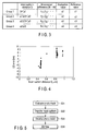
- FIG. 3 is a table to explain groups according to an embodiment of the present invention.
- FIG. 4 is a graph showing the relationship between an inter-pattern distance and a CD error according to an embodiment of the present invention.
- FIG. 5 is a flowchart to schematically explain a method of manufacturing a semiconductor device according to an embodiment of the present invention.
- FIG. 1 is a flowchart to explain a method of evaluating a photo mask according to an embodiment of the present invention.
- a photo mask formed with a mask pattern is prepared (S 11 ).
- Optical proximity correction (OPC) and process proximity correction (PPC) are made with respect to a mask pattern formed on a photo mask.
- the dimension of a plurality of pattern portions (measurement target pattern portions) of the mask pattern formed on the photo mask is measured (S 12 ).
- a mask pattern dimension is measured at a plurality of portions on the photo mask.
- a pattern width W of a measurement target pattern portion 11 is measured.
- An inter-pattern distance between the measurement target pattern portion and a pattern neighboring there is measured with respect to each of a plurality of measurement target pattern portions (S 13 ).
- the following inter-pattern distances (inter-edge distance) D 1 and D 2 are measured.
- the foregoing D 1 is an inter-pattern distance between the measurement target pattern portion 11 and a neighboring pattern 21 .
- the foregoing D 2 is an inter-pattern distance between the measurement target pattern portion 11 and a neighboring pattern 22 .
- the foregoing average inter-pattern distance D is used as an inter-pattern distance, as far as reference is not specially made.
- the foregoing pattern width W. inter-pattern distances D 1 and D 2 can be determined from an image obtained by an electron microscope.
- the inter-pattern distance is not necessarily determined using the distance between neighboring patterns.
- a value is defined based on a distance between a predetermined measurement target pattern and any pattern different from the predetermined pattern.
- the defined value may be defined as an inter-pattern distance of the predetermined pattern. For example, each inter-pattern distance between the predetermined pattern and a plurality of peripheral patterns different from the predetermined pattern is measured. Based on the measured value, a value expressing pattern density may be regarded as an inter-pattern distance.
- ) between the measured dimension of the measurement target pattern portion (dimension W obtained in step S 12 ) and a target dimension Wt thereof is calculated with respect to each of the measurement target pattern portions (S 14 ).
- the target dimension Wt expressing a pattern dimension to be formed on a mask is previously determined by calculation. For example, based on mask pattern writing data, the target dimension Wt is previously calculated.
- the dimensional difference obtained for each measurement target pattern portion is grouped into a plurality of groups in accordance with the inter-pattern distance obtained for each measurement target pattern portion (S 15 ).
- FIG. 3 is a table to explain the foregoing groups. As seen from the table of FIG. 3 , the dimensional difference is grouped into four groups 1 to 4 in accordance with the inter-pattern distance D. Hereinafter, the detailed explanation will be made.
- an inter-pattern distance D of a measurement target pattern portion P 1 is D ⁇ a 1 (a 1 is a predetermined boundary value)
- ) of the portion P 1 is assigned to a group 1.
- an inter-pattern distance D of a measurement target pattern portion P 2 is a 1 ⁇ D ⁇ a 2 (a 1 and a 2 are a predetermined boundary value)
- ) of the portion P 2 is assigned to a group 2.
- dimensional differences are assigned to group 3 and group 4 in accordance with an inter-pattern distance.
- (in FIG. 3 , dimensional difference f 11 , f 12 , . . . ) of the measurement target pattern portion having the inter-pattern distance D (D ⁇ a 1 ) is set to the group 1.
- the dimensional difference (in FIG. 3 , dimensional difference f 21 , f 22 , . . . ) of the measurement target pattern portion having the inter-pattern distance D (a 1 ⁇ D ⁇ a 2 ) is set to the group 2.
- the dimensional difference (in FIG. 3 , dimensional difference f 31 , f 32 , . . .
- the dimensional difference (in FIG. 3 , dimensional difference f 41 , f 42 , . . . ) of the measurement target pattern portion having the inter-pattern distance D (a 3 ⁇ D) is set to the group 4.
- FIG. 4 is a graph plotting the relationship between the inter-pattern distance D and a CD error (corresponding to dimensional difference between measured dimension and target dimension) with respect to actual mask patterns.
- D inter-pattern distance
- a CD error corresponding to dimensional difference between measured dimension and target dimension
- An evaluation value based on the dimensional difference in each group is determined with respect to each of the foregoing groups (groups 1 to 4) (S 16 ).
- a value expressing variations of measurement dimension with respect to the target dimension is usable as the evaluation value.
- a value expressing an average of the dimensional differences in the group is usable as the evaluation value.
- root mean square (rms) of the dimensional differences in the group is used as the evaluation value.
- evaluation values e 2 , e 3 and e 4 of groups 2, 3 and 4 are expressed in the same manner as described above.
- a photo mask is evaluated based on the evaluation value obtained in step S 16 (S 17 ). Specifically, it is determined whether or not the evaluation value satisfies an evaluation criterion for each group.
- the explanation will be made below using FIG. 3 .
- the group 1 it is determined whether or not the evaluation value e 1 is smaller than a predetermined reference value c 1 . If the evaluation value e 1 is smaller than the reference value c 1 , in the group 1, it is determined that the evaluation value satisfies the evaluation criterion.
- the evaluation value e 2 is smaller than a reference value c 2 , it is determined that the evaluation value satisfies the evaluation criterion.
- the same determination as above is made in the groups 3 and 4.
- the foregoing reference values (c 1 to c 4 ) are set for each group in accordance with the inter-pattern distance. In the groups having a larger inter-pattern distance D, the reference value is set larger. Based on the evaluation result, it is determined whether or not a photo mask is acceptable. For example, in all groups (groups 1 to 4), if it is determined that the evaluation value satisfies the evaluation criterion, it is determined that the photo mask is acceptable.
- the dimensional difference (between measured dimension and target dimension) obtained for each measurement target pattern portion is grouped into a plurality of groups in accordance with the inter-pattern distance obtained for each measurement target pattern portion. Further, the evaluation value based on the dimensional difference is obtained for each group.
- the method described above is employed, and thereby, according to this embodiment, it is possible to accurately evaluate the photo mask. Therefore, it is possible to accurately determine whether or not the photo mask is acceptable. The explanation will be additionally made below.
- photolithography margin is taken in the following manner. Specifically, photolithography margin is taken larger at a portion having a large inter-pattern distance D. Conversely, the photolithography margin is taken smaller at a portion having a small inter-pattern distance D. Therefore, the dimensional difference between measured dimension and target dimension may be larger to some degree at a portion having a large inter-pattern distance D. However, the dimensional difference between measured dimension and target dimension must be set so that it does not become large at a portion having a small inter-pattern distance D. In other words, the evaluation value of the dimensional difference may be relatively larger at a portion having a large inter-pattern distance D, compared with a portion having a small inter-pattern distance D.
- the evaluation value of the dimensional difference is obtained for each group in accordance with the inter-pattern distance. As a result, it is possible to make a rational evaluation, and to accurately evaluate the photo mask.
- FIG. 5 is a flowchart to schematically explain a method of manufacturing a semiconductor device.
- the foregoing method is used to evaluate a photo mask (S 31 ).
- a mask pattern on a photo mask is transferred to a photo resist on a semiconductor wafer using the photo mask determined as acceptable (S 32 ).
- the photo resist is developed to form a photo resist pattern (S 33 ).
- etching is carried out using the photo resist pattern as a mask, and a pattern is formed on the semiconductor wafer (S 34 ).
Landscapes
- Physics & Mathematics (AREA)
- General Physics & Mathematics (AREA)
- Preparing Plates And Mask In Photomechanical Process (AREA)
- Exposure And Positioning Against Photoresist Photosensitive Materials (AREA)
Abstract
Description
e1={(f 11 2 +f 12 2 + . . . +f 1n 2)/n} 1/2
Claims (13)
Applications Claiming Priority (2)
| Application Number | Priority Date | Filing Date | Title |
|---|---|---|---|
| JP2008-018034 | 2008-01-29 | ||
| JP2008018034A JP2009180824A (en) | 2008-01-29 | 2008-01-29 | Photomask evaluation method and semiconductor device manufacturing method |
Publications (2)
| Publication Number | Publication Date |
|---|---|
| US20090202924A1 US20090202924A1 (en) | 2009-08-13 |
| US7912275B2 true US7912275B2 (en) | 2011-03-22 |
Family
ID=40939162
Family Applications (1)
| Application Number | Title | Priority Date | Filing Date |
|---|---|---|---|
| US12/360,929 Active 2029-07-30 US7912275B2 (en) | 2008-01-29 | 2009-01-28 | Method of evaluating a photo mask and method of manufacturing a semiconductor device |
Country Status (2)
| Country | Link |
|---|---|
| US (1) | US7912275B2 (en) |
| JP (1) | JP2009180824A (en) |
Families Citing this family (3)
| Publication number | Priority date | Publication date | Assignee | Title |
|---|---|---|---|---|
| JP2011137901A (en) * | 2009-12-28 | 2011-07-14 | Hitachi High-Technologies Corp | Apparatus for setting pattern measuring condition |
| JP2012068454A (en) * | 2010-09-24 | 2012-04-05 | Toshiba Corp | Pattern shape determining method, pattern shape verifying method, pattern correcting method, method of manufacturing mask for lithography, and method of manufacturing semiconductor device |
| JP6428555B2 (en) * | 2014-10-24 | 2018-11-28 | 信越化学工業株式会社 | Method for evaluating defect size of photomask blank, selection method and manufacturing method |
Citations (2)
| Publication number | Priority date | Publication date | Assignee | Title |
|---|---|---|---|---|
| JP2003241364A (en) | 2002-02-15 | 2003-08-27 | Toppan Printing Co Ltd | Photomask pattern dimension assurance system |
| US20060190875A1 (en) | 2005-01-07 | 2006-08-24 | Yukiyasu Arisawa | Pattern extracting system, method for extracting measuring points, method for extracting patterns, and computer program product for extracting patterns |
Family Cites Families (3)
| Publication number | Priority date | Publication date | Assignee | Title |
|---|---|---|---|---|
| JP4131880B2 (en) * | 1997-07-31 | 2008-08-13 | 株式会社東芝 | Mask data creation method and mask data creation apparatus |
| JP2002296761A (en) * | 2001-03-29 | 2002-10-09 | Toshiba Corp | Pattern measuring method and pattern measuring device |
| JP3825744B2 (en) * | 2002-12-02 | 2006-09-27 | 株式会社東芝 | Photomask manufacturing method and semiconductor device manufacturing method |
-
2008
- 2008-01-29 JP JP2008018034A patent/JP2009180824A/en active Pending
-
2009
- 2009-01-28 US US12/360,929 patent/US7912275B2/en active Active
Patent Citations (2)
| Publication number | Priority date | Publication date | Assignee | Title |
|---|---|---|---|---|
| JP2003241364A (en) | 2002-02-15 | 2003-08-27 | Toppan Printing Co Ltd | Photomask pattern dimension assurance system |
| US20060190875A1 (en) | 2005-01-07 | 2006-08-24 | Yukiyasu Arisawa | Pattern extracting system, method for extracting measuring points, method for extracting patterns, and computer program product for extracting patterns |
Also Published As
| Publication number | Publication date |
|---|---|
| JP2009180824A (en) | 2009-08-13 |
| US20090202924A1 (en) | 2009-08-13 |
Similar Documents
| Publication | Publication Date | Title |
|---|---|---|
| KR102411813B1 (en) | Method to predict yield of a device manufacturing process | |
| CN113168116B (en) | Method for determining root causes affecting yield in semiconductor manufacturing processes | |
| KR100498197B1 (en) | Photomask, focus monitoring method, method for monitoring light exposure and method for fabricating semiconductor device | |
| KR100541898B1 (en) | Manufacturing method of photomask and manufacturing method of semiconductor device | |
| US20030156276A1 (en) | Aberration mark and method for estimating overlay error and optical aberrations | |
| US8261214B2 (en) | Pattern layout creation method, program product, and semiconductor device manufacturing method | |
| CN104736962A (en) | Method for estimating and correcting misregistration target inaccuracy | |
| US20090310116A1 (en) | Recording medium storing program for determining exposure parameter, exposure method, and method of manufacturing device | |
| US20080209386A1 (en) | Method for predicting resist pattern shape, computer readable medium storing program for predicting resist pattern shape, and computer for predicting resist pattern shape | |
| WO2004013696A1 (en) | Pattern size correcting device and pattern size correcting method | |
| KR20080045067A (en) | Mask Pattern Correction Program and Mask Pattern Correction System | |
| CN116224718B (en) | Overlay error compensation method and system, and computer-readable storage medium | |
| CN114117573B (en) | Method for processing auxiliary graphics using visual editing graphics database | |
| KR102904615B1 (en) | Method of determining set of sample shot regions, method of obtaining measurement value, information processing apparatus, lithography apparatus, program, and article manufacturing method | |
| US7912275B2 (en) | Method of evaluating a photo mask and method of manufacturing a semiconductor device | |
| US8443309B2 (en) | Multifeature test pattern for optical proximity correction model verification | |
| TWI421908B (en) | Method for constructing opc model | |
| US7952696B2 (en) | Exposure measurement method and apparatus, and semiconductor device manufacturing method | |
| KR20090000868A (en) | Optical proximity effect correction method | |
| KR101160010B1 (en) | Method for processing optical proximity correction | |
| JP5087928B2 (en) | Yield calculation method for semiconductor device and computer program | |
| JP4483612B2 (en) | Photomask manufacturing method and semiconductor device manufacturing method | |
| US10748821B2 (en) | Method and system for measuring pattern placement error on a wafer | |
| US20060206853A1 (en) | Method of producing mask inspection data, method of manufacturing a photo mask and method of manufacturing a semiconductor device | |
| EP4372468A1 (en) | A method for optimizing a parameter applied in a semiconductor fabrication process including a lithography step |
Legal Events
| Date | Code | Title | Description |
|---|---|---|---|
| AS | Assignment |
Owner name: KABUSHIKI KAISHA TOSHIBA, JAPAN Free format text: ASSIGNMENT OF ASSIGNORS INTEREST;ASSIGNORS:YAMAMOTO, HIROKI;ITOH, MASAMITSU;IKENAGA, OSAMU;AND OTHERS;REEL/FRAME:022538/0701;SIGNING DATES FROM 20090209 TO 20090227 Owner name: KABUSHIKI KAISHA TOSHIBA, JAPAN Free format text: ASSIGNMENT OF ASSIGNORS INTEREST;ASSIGNORS:YAMAMOTO, HIROKI;ITOH, MASAMITSU;IKENAGA, OSAMU;AND OTHERS;SIGNING DATES FROM 20090209 TO 20090227;REEL/FRAME:022538/0701 |
|
| STCF | Information on status: patent grant |
Free format text: PATENTED CASE |
|
| FEPP | Fee payment procedure |
Free format text: PAYOR NUMBER ASSIGNED (ORIGINAL EVENT CODE: ASPN); ENTITY STATUS OF PATENT OWNER: LARGE ENTITY |
|
| FPAY | Fee payment |
Year of fee payment: 4 |
|
| AS | Assignment |
Owner name: TOSHIBA MEMORY CORPORATION, JAPAN Free format text: ASSIGNMENT OF ASSIGNORS INTEREST;ASSIGNOR:KABUSHIKI KAISHA TOSHIBA;REEL/FRAME:043709/0035 Effective date: 20170706 |
|
| MAFP | Maintenance fee payment |
Free format text: PAYMENT OF MAINTENANCE FEE, 8TH YEAR, LARGE ENTITY (ORIGINAL EVENT CODE: M1552); ENTITY STATUS OF PATENT OWNER: LARGE ENTITY Year of fee payment: 8 |
|
| AS | Assignment |
Owner name: K.K. PANGEA, JAPAN Free format text: MERGER;ASSIGNOR:TOSHIBA MEMORY CORPORATION;REEL/FRAME:055659/0471 Effective date: 20180801 Owner name: TOSHIBA MEMORY CORPORATION, JAPAN Free format text: CHANGE OF NAME AND ADDRESS;ASSIGNOR:K.K. PANGEA;REEL/FRAME:055669/0401 Effective date: 20180801 Owner name: KIOXIA CORPORATION, JAPAN Free format text: CHANGE OF NAME AND ADDRESS;ASSIGNOR:TOSHIBA MEMORY CORPORATION;REEL/FRAME:055669/0001 Effective date: 20191001 |
|
| MAFP | Maintenance fee payment |
Free format text: PAYMENT OF MAINTENANCE FEE, 12TH YEAR, LARGE ENTITY (ORIGINAL EVENT CODE: M1553); ENTITY STATUS OF PATENT OWNER: LARGE ENTITY Year of fee payment: 12 |