US7902946B2 - MEMS relay with a flux path that is decoupled from an electrical path through the switch and a suspension structure that is independent of the core structure and a method of forming the same - Google Patents

MEMS relay with a flux path that is decoupled from an electrical path through the switch and a suspension structure that is independent of the core structure and a method of forming the same Download PDF

Info

Publication number
US7902946B2
US7902946B2 US12/218,368 US21836808A US7902946B2 US 7902946 B2 US7902946 B2 US 7902946B2 US 21836808 A US21836808 A US 21836808A US 7902946 B2 US7902946 B2 US 7902946B2
Authority
US
United States
Prior art keywords
conductive
magnetic member
forming
coil
layer
Prior art date
Legal status (The legal status is an assumption and is not a legal conclusion. Google has not performed a legal analysis and makes no representation as to the accuracy of the status listed.)
Active, expires
Application number
US12/218,368
Other versions
US20100007448A1 (en
Inventor
Trevor Niblock
Current Assignee (The listed assignees may be inaccurate. Google has not performed a legal analysis and makes no representation or warranty as to the accuracy of the list.)
National Semiconductor Corp
Original Assignee
National Semiconductor Corp
Priority date (The priority date is an assumption and is not a legal conclusion. Google has not performed a legal analysis and makes no representation as to the accuracy of the date listed.)
Filing date
Publication date
Application filed by National Semiconductor Corp filed Critical National Semiconductor Corp
Assigned to NATIONAL SEMICONDUCTOR CORPORATION reassignment NATIONAL SEMICONDUCTOR CORPORATION ASSIGNMENT OF ASSIGNORS INTEREST (SEE DOCUMENT FOR DETAILS). Assignors: NIBLOCK, TREVOR
Priority to US12/218,368 priority Critical patent/US7902946B2/en
Priority to TW098122170A priority patent/TWI492259B/en
Priority to DE112009001086T priority patent/DE112009001086T5/en
Priority to KR1020107023829A priority patent/KR101724717B1/en
Priority to PCT/US2009/049675 priority patent/WO2010005888A2/en
Priority to JP2011517499A priority patent/JP5456777B2/en
Publication of US20100007448A1 publication Critical patent/US20100007448A1/en
Publication of US7902946B2 publication Critical patent/US7902946B2/en
Application granted granted Critical
Active legal-status Critical Current
Adjusted expiration legal-status Critical

Links

Images

Classifications

    • HELECTRICITY
    • H01ELECTRIC ELEMENTS
    • H01HELECTRIC SWITCHES; RELAYS; SELECTORS; EMERGENCY PROTECTIVE DEVICES
    • H01H50/00Details of electromagnetic relays
    • H01H50/005Details of electromagnetic relays using micromechanics
    • HELECTRICITY
    • H01ELECTRIC ELEMENTS
    • H01HELECTRIC SWITCHES; RELAYS; SELECTORS; EMERGENCY PROTECTIVE DEVICES
    • H01H59/00Electrostatic relays; Electro-adhesion relays
    • BPERFORMING OPERATIONS; TRANSPORTING
    • B81MICROSTRUCTURAL TECHNOLOGY
    • B81BMICROSTRUCTURAL DEVICES OR SYSTEMS, e.g. MICROMECHANICAL DEVICES
    • B81B3/00Devices comprising flexible or deformable elements, e.g. comprising elastic tongues or membranes
    • HELECTRICITY
    • H01ELECTRIC ELEMENTS
    • H01HELECTRIC SWITCHES; RELAYS; SELECTORS; EMERGENCY PROTECTIVE DEVICES
    • H01H3/00Mechanisms for operating contacts
    • H01H3/22Power arrangements internal to the switch for operating the driving mechanism
    • H01H3/28Power arrangements internal to the switch for operating the driving mechanism using electromagnet
    • HELECTRICITY
    • H01ELECTRIC ELEMENTS
    • H01HELECTRIC SWITCHES; RELAYS; SELECTORS; EMERGENCY PROTECTIVE DEVICES
    • H01H49/00Apparatus or processes specially adapted to the manufacture of relays or parts thereof
    • HELECTRICITY
    • H01ELECTRIC ELEMENTS
    • H01HELECTRIC SWITCHES; RELAYS; SELECTORS; EMERGENCY PROTECTIVE DEVICES
    • H01H51/00Electromagnetic relays
    • H01H51/02Non-polarised relays
    • H01H51/04Non-polarised relays with single armature; with single set of ganged armatures
    • H01H51/06Armature is movable between two limit positions of rest and is moved in one direction due to energisation of an electromagnet and after the electromagnet is de-energised is returned by energy stored during the movement in the first direction, e.g. by using a spring, by using a permanent magnet, by gravity
    • YGENERAL TAGGING OF NEW TECHNOLOGICAL DEVELOPMENTS; GENERAL TAGGING OF CROSS-SECTIONAL TECHNOLOGIES SPANNING OVER SEVERAL SECTIONS OF THE IPC; TECHNICAL SUBJECTS COVERED BY FORMER USPC CROSS-REFERENCE ART COLLECTIONS [XRACs] AND DIGESTS
    • Y10TECHNICAL SUBJECTS COVERED BY FORMER USPC
    • Y10TTECHNICAL SUBJECTS COVERED BY FORMER US CLASSIFICATION
    • Y10T29/00Metal working
    • Y10T29/49Method of mechanical manufacture
    • Y10T29/49002Electrical device making
    • Y10T29/49105Switch making

Definitions

  • the present invention relates to relays and, more particularly, to a MEMS relay that has a flux path from magnetic actuation that is decoupled from an electrical path through the switch, and a suspension structure that is independent of the core structure, and a method of forming the same.
  • a switch is a well-known device that connects, disconnects, or changes connections between devices.
  • An electrical switch is a switch that provides a low-impedance electrical pathway when the switch is “closed,” and a high-impedance electrical pathway when the switch is “opened.”
  • a mechanical-electrical switch is a type of switch where the low-impedance electrical pathway is formed by physically bringing two electrical contacts together, and the high-impedance electrical pathway is formed by physically separating the two electrical contacts from each other.
  • An actuator is a well-known mechanical device that moves or controls a mechanical member to move or control another device.
  • Actuators are commonly used with mechanical-electrical switches to move or control a mechanical member that closes and opens the switch, thereby providing the low-impedance and high-impedance electrical pathways, respectively, in response to the actuator.
  • a relay is a combination of a switch and an actuator where the mechanical member in the actuator moves in response to electromagnetic changes in the conditions of an electrical circuit. For example, electromagnetic changes due to the presence or absence of a current in a coil can cause the mechanical member in the actuator to close and open the switch.
  • MEMS micro-electromechanical system
  • MEMS relays are passing signals with very small amplitudes through the switch, fluctuations in the current around the core and, thereby the flux, can lead to an unacceptable degradation of the signal passing through the switch.
  • a MEMS relay that has a flux path that is decoupled from the electrical path through the switch.
  • the suspension structure is typically formed as part of the core structure.
  • the suspension and core structures commonly have conflicting requirements.
  • the ideal geometry of the core structure is a short flux path with a large cross-sectional area.
  • the ideal geometry of the suspension structure is a long path with a small cross-sectional area because this reduces the spring stiffness of the beam, and thus the force required to close the switch.
  • FIGS. 2A-15A , 2 B- 15 B, 2 C- 15 C, 2 D- 15 D, and 2 E- 15 E are a series of views that illustrate an example of method 100 in accordance with the present invention.
  • FIGS. 2A-15A are plan views.
  • FIGS. 2B-15B are cross-sectional views taken along lines 2 B- 2 B of FIGS. 2 A through 15 B- 15 B of FIG. 15A , respectively.
  • FIGS. 2C-15C are cross-sectional views taken along lines 2 C- 2 C of FIGS. 2 A through 15 C- 15 C of FIG. 15A , respectively.
  • FIGS. 2D-15D are cross-sectional views taken along lines 2 D- 2 D of FIGS. 2 A through 15 D- 15 D of FIG. 15A , respectively.
  • FIGS. 2E-15E are cross-sectional views taken along lines 2 E- 2 E of FIGS. 2 A through 15 E- 15 E of FIG. 15A , respectively.
  • FIGS. 16A-18A , 16 B- 18 B, 16 C- 18 C, 16 D- 18 D, and 16 E- 18 E are a series of views illustrating a first example of an alternate way of implementing element 110 of method 100 in accordance with the present invention.
  • FIGS. 16A-18A are plan views.
  • FIGS. 16B-18B are cross-sectional views taken along lines 16 B- 16 B of FIG. 16 A through 18 B- 18 B of FIG. 18A , respectively.
  • FIGS. 16C-18C are cross-sectional views taken along lines 16 C- 16 C of FIG. 16 A through 18 C- 18 C of FIG. 18A , respectively.
  • FIGS. 16D-18D are cross-sectional views taken along lines 16 D- 16 D of FIG. 16 A through 18 D- 18 D of FIG. 18A , respectively.
  • FIGS. 16E-18E are cross-sectional views taken along lines 16 E- 16 E of FIG. 16 A through 18 E- 18 E of FIG. 18A , respectively.
  • FIGS. 19A-21A , 19 B- 21 B, 19 C- 21 C, 19 D- 21 D, and 19 E- 21 E are a series of views illustrating a second example of an alternate way of implementing element 110 of method 100 in accordance with the present invention.
  • FIGS. 19A-21A are plan views.
  • FIGS. 19B-21B are cross-sectional views taken along lines 19 B- 19 B of FIG. 19 A through 21 B- 21 B of FIG. 21A , respectively.
  • FIGS. 19C-21C are cross-sectional views taken along lines 19 C- 19 C of FIG. 19 A through 21 C- 21 C of FIG. 21A , respectively.
  • FIGS. 19D-21D are cross-sectional views taken along lines 19 D- 19 D of FIG. 19 A through 21 D- 21 D of FIG. 21A , respectively.
  • FIGS. 19E-21E are cross-sectional views taken along lines 19 E- 19 E of FIG. 19 A through 21 E- 21 E of FIG. 21A , respectively.
  • FIGS. 22A-26A , 22 B- 26 B, 22 C- 26 C, 22 D- 26 D, and 22 E- 26 E are a series of views illustrating an example of an alternate way of implementing element 118 of method 100 in accordance with the present invention.
  • FIGS. 22A-26A are plan views.
  • FIGS. 22B-26B are cross-sectional views taken along lines 22 B- 22 B of FIG. 22 A through 26 B- 26 B of FIG. 26A , respectively.
  • FIGS. 22C-26C are cross-sectional views taken along lines 22 C- 22 C of FIG. 22 A through 26 C- 26 C of FIG. 26A , respectively.
  • FIGS. 22D-26D are cross-sectional views taken along lines 22 D- 22 D of FIG. 22 A through 26 D- 26 D of FIG. 26A , respectively.
  • FIGS. 22E-26E are cross-sectional views taken along lines 22 E- 22 E of FIG. 22 A through 26 E- 26 E of FIG. 26A , respectively
  • FIGS. 28A-28E are a series of views illustrating an example of sacrificial structure 230 , core 236 , intermediate member 246 , and spring member 254 with a different shape in accordance with the present invention.
  • the present invention is a MEMS relay, and a method of forming the relay, that has a flux path from magnetic actuation which is decoupled from the electrical path through the switch.
  • the MEMS relay has a suspension structure that is independent of the core structure.
  • FIG. 1 shows an example of a method 100 of forming the MEMS relay in accordance with the present invention.
  • method 100 begins in 110 by forming a number of spaced-apart lower coil members that form the lower horizontal sections of a to-be-formed coil.
  • a pair of lower input/output members can optionally be formed at the same time that the lower coil members are formed.
  • FIGS. 2A-15A , 2 B- 15 B, 2 C- 15 C, 2 D- 15 D, and 2 E- 15 E show a series of views that illustrate an example of method 100 in accordance with the present invention.
  • FIGS. 2A-3A , 2 B- 3 B, 2 C- 3 C, 2 D- 3 D, and 2 E- 3 E show a series of views that illustrate an example of method 100 forming a number of spaced-apart lower coil members in accordance with the present invention.
  • method 100 utilizes a conventionally formed single-crystal silicon semiconductor wafer 210 that has an overlying base dielectric layer 212 .
  • Base dielectric layer 212 can represent a dielectric layer that includes no metal structures, or a dielectric layer that includes metal structures, such as the dielectric layer of a metal interconnect structure.
  • base dielectric layer 212 When formed as the dielectric layer of a metal interconnect structure, base dielectric layer 212 includes levels of metal traces, which are typically aluminum, a large number of contacts that connect the bottom metal trace to electrically conductive regions on wafer 210 , and a large number of inter-metal vias that connect the metal traces in adjacent layers together. Further, selected regions on the top surfaces of the metal traces in the top metal layer function as pads which provide external connection points.
  • base dielectric layer 212 represents the dielectric layer of a metal interconnect structure that also includes pads P 1 -P 4 .
  • Pads P 1 and P 2 are selected regions on the top surfaces of two of the metal traces in the top layer of metal traces that provide electrical connections for a to-be-formed coil, while pads P 3 and P 4 are selected regions on the top surfaces of the metal traces that provide electrical input/output connections for a to-be-formed switch. (Only pads P 1 -P 4 , and not the entire metal interconnect structure, are shown in cross-section for clarity.)
  • method 100 begins by forming a metal layer 214 on the top surface of base dielectric layer 212 .
  • metal layer 214 is also formed on the top surfaces of the pads P 1 -P 4 .
  • Metal layer 214 can include, for example, a layer of titanium (e.g., 100 ⁇ thick), a layer of titanium nitride (e.g., 200 ⁇ thick), a layer of aluminum copper (e.g., 1.2 ⁇ m thick), a layer of titanium (e.g., 44 ⁇ thick), and a layer of titanium nitride (e.g., 250 ⁇ thick).
  • a lower mask 216 is formed and patterned on the top surface of metal layer 214 .
  • metal layer 214 is etched to remove the exposed regions of metal layer 214 and form a number of spaced-apart lower coil members 220 .
  • the lower coil members 220 which have a horseshoe shape, form the lower sides of the to-be-formed coil. Since base dielectric layer 212 represents the dielectric layer of a metal interconnect structure in the present example, the ends of the lower coil members 220 that correspond with the opposite ends of the to-be-formed coil are physically and electrically connected to pads P 1 and P 2 .
  • the etch can optionally form a pair of lower input/output members 222 that are physically and electrically connected to the input/output pads P 3 and P 4 .
  • mask 216 is removed.
  • method 100 moves to 112 to form a lower dielectric layer that touches the lower coil members and the pair of input/output members.
  • FIGS. 4A , 4 B, 4 C, 4 D, and 4 E show a series of views that illustrate an example of method 100 forming a lower dielectric layer in accordance with the present invention.
  • a lower dielectric layer 224 such as an oxide layer, is formed on base dielectric layer 212 , the lower coil members 220 , and the pair of lower input/output members 222 .
  • lower dielectric layer can be formed by depositing an oxide, and then chemically-mechanically polishing the oxide to have, for example, a target thickness of, for example, 2000 ⁇ , over base dielectric layer 212 .
  • method 100 moves to 114 to form a sacrificial structure that touches the lower dielectric layer.
  • FIGS. 5A-6A , 5 B- 6 B, 5 C- 6 C, 5 D- 6 D, and 5 E- 6 E show a series of views that illustrate an example of method 100 forming a sacrificial structure in accordance with the present invention.
  • a sacrificial layer 226 is formed on the top surface of lower dielectric layer 224 .
  • a layer of amorphous silicon that has a thickness of, for example, 2000 ⁇ , can be formed on the top surface of lower dielectric layer 224 .
  • a mask 228 is formed and patterned on the top surface of sacrificial layer 226 .
  • sacrificial layer 226 is etched to remove the exposed regions of sacrificial layer 226 and form a sacrificial structure 230 .
  • mask 228 is removed.
  • method 100 moves to 116 to form a core, a switch member, and a suspension member that touch the lower dielectric layer. No portion of the switch member touches the core.
  • FIGS. 7A-9A , 7 B- 9 B, 7 C- 9 C, 7 D- 9 D, and 7 E- 9 E show a series of views that illustrate an example of method 100 forming a core, a switch member, and a suspension member in accordance with the present invention.
  • a seed layer 232 is formed on the top surface of lower dielectric layer 224 and sacrificial structure 230 .
  • seed layer can be formed by depositing 300 ⁇ of titanium, 3000 ⁇ of copper, and 300 ⁇ of titanium.
  • a plating mold 234 (shown cross-hatched) is formed and patterned on the top surface of seed layer 232 .
  • the top titanium layer is stripped and a magnetic material, such as an alloy of nickel and iron like permalloy, is deposited by electroplating to a thickness of, for example, 10 ⁇ m, to form a core 236 , a switch member 238 , and a suspension member 240 .
  • a magnetic material such as an alloy of nickel and iron like permalloy
  • plating mold 234 is removed, followed by the removal of the underlying regions of seed layer 232 .
  • core 236 which mirrors the shape of the to-be-formed coil, also has a horseshoe shape that lies over the lower coil members 220 , while switch member 238 has a contact sidewall 244 .
  • suspension member 240 has an intermediate member 246 .
  • Intermediate member 246 lies between core 236 and switch member 238 , and lies adjacent to the contact sidewall 244 of switch member 238 .
  • intermediate member 246 is separated from core 236 by an actuation gap 250
  • intermediate member 246 is separated from the contact sidewall 244 of switch member 238 by a contact gap 252 .
  • Actuation gap 250 can be made to be slightly larger than contact gap 252 , thereby ensuring that an electrical connection will always be made when the relay is activated.
  • the sizes of actuation gap 250 and contact gap 252 are defined by the pattern in plating mold 234 .
  • intermediate member 246 is also formed to have a half-circle shape, and is oriented towards core 236 to form a racetrack shape.
  • Suspension member 240 also includes a spring member 254 . In the present example, as shown in FIGS.
  • spring member 254 is implemented with a base section 256 , which provides the only point where suspension member 240 touches lower dielectric layer 224 , and an extension section 260 that, along with intermediate member 246 , are spaced apart from dielectric layer 224 .
  • method 100 moves to 118 to form tops and sides that touch the lower coil members to form a coil, a conductive first switch trace that sits over the switch member, and a conductive second switch trace that sits over and rides on the suspension member. No portion of the coil is wrapped around the suspension member.
  • FIGS. 10A-14A , 10 B- 14 B, 10 C- 14 C, 10 D- 14 D, and 10 E- 14 E show a series of views that illustrate an example of method 100 forming tops and sides that touch the lower coil members to form a coil, a conductive first switch trace that sits over the switch member, and a conductive second switch trace that sits over and rides on the suspension member in accordance with the present invention.
  • an upper dielectric layer 262 such as an oxide layer, is formed on lower dielectric layer 224 , core 236 , switch member 238 , and suspension member 240 .
  • upper dielectric layer 262 can be formed by conformally depositing an oxide to a thickness of, for example, 1 ⁇ m, over lower dielectric layer 224 .
  • a mask 264 such as a layer of photoresist, is then formed and patterned on the top surface of upper dielectric layer 262 .
  • the exposed regions of the upper dielectric layer 262 and underlying lower dielectric layer 224 are etched to form a number of vertical openings 266 .
  • the vertical openings 266 include via-type openings that expose the top surfaces of the ends of the lower coil members 220 that form the lower sides of the to-be-formed coil.
  • the vertical openings 266 also expose the pair of lower input/output members 222 .
  • the vertical openings 266 also form a trench that extends from base section 256 around suspension member 240 and back again to base section 256 .
  • the exposed regions of sacrificial structure 230 are not to be removed during this etch.
  • vertical openings 266 are formed with an etchant that is highly selective to the material used to form sacrificial structure 230 .
  • sacrificial structure 230 which was formed to have the same thickness as lower dielectric layer 224 , can also be formed to be thicker than lower dielectric layer 224 to ensure that a significant portion of the exposed regions of sacrificial structure 230 remain after the etch. Following the etch, mask 264 is then removed.
  • a seed layer 270 is formed on the exposed ends of the lower coil members 220 , the exposed input/output members 222 , lower dielectric layer 224 , sacrificial structure 230 , and the top surface of upper dielectric layer 262 .
  • seed layer can be formed by depositing 300 ⁇ of titanium, 3000 ⁇ of copper, and 300 ⁇ of titanium.
  • a plating mold 272 (shown cross-hatched) is formed and patterned on the top surface of seed layer 270 . The pattern in plating mold 272 is shown hatched in FIG. 12A .
  • the top titanium layer is stripped and copper is deposited by electroplating to form a number of copper side sections 274 of the coil, and a number of copper upper sections 276 of the coil.
  • the electroplating also forms a first switch trace 280 with a sidewall contact 282 , and a second switch trace 284 with a sidewall contact 286 .
  • the first and second switch traces 280 and 284 also touch the input/output members 222 to make an electrical connection.
  • lower coil member 220 - 1 , side section 274 - 1 , and upper section 276 - 1 form three sides of one coil loop. Following this, as shown in FIGS. 14A-14E , plating mold 272 and the underlying regions of seed layer 270 are removed.
  • method 100 moves to 120 to remove the sacrificial structure so that the suspension member moves in response to changes in a current flowing through the coil.
  • the conductive second switch trace makes and breaks electrical contact with the first conductive switch trace as the suspension member moves in response to changes in a current flowing through the coil.
  • a magnetic flux passes through a portion of the suspension member and substantially no magnetic flux passes through the first and the second conductive switch traces when a current flows through the coil.
  • FIGS. 15A-15E show a series of views that illustrate an example of method 100 removing sacrificial structure 230 in accordance with the present invention.
  • sacrificial structure 230 is removed.
  • the removal of sacrificial structure 230 leaves intermediate member 246 and extension section 260 of spring member 254 floating.
  • intermediate member 246 and extension section 260 each float, connected to lower dielectric layer 224 only via base section 256 .
  • Floating extension section 260 was vertically spaced apart from lower dielectric layer 224 by underlying sacrificial structure 230 , and thereby floats after underlying sacrificial structure 230 has been removed. As a result, the thickness of sacrificial structure 230 determines an offset gap 290 , which is the vertical spacing that lies between lower dielectric layer 224 and floating extension section 260 .
  • the method of the present invention forms a MEMS relay 1500 that includes core 236 and a coil 1510 that is wrapped around core 236 .
  • Coil 1510 can be implemented with the lower coil members 220 , the copper side sections 274 , and the copper upper sections 276 .
  • both core 236 and coil 1510 touch lower dielectric layer 224 .
  • MEMS relay 1500 also includes a switch structure 1512 and a suspension structure 1514 .
  • Switch structure 1512 can be implemented with switch member 238 , which touches lower dielectric layer 224 , and upper dielectric layer 262 .
  • Suspension structure 1514 can be implemented with suspension member 240 , which touches lower dielectric layer 224 , and upper dielectric layer 262 . Further, no portion of coil 1510 is wrapped around suspension structure 1514 .
  • MEMS relay 1500 includes first switch trace 280 that touches and extends along switch structure 1512 , and second switch trace 284 that touches and extends along suspension structure 1514 . Further, first switch trace 280 has a first sidewall contact 282 , and second switch trace 284 has a second sidewall contact 286 .
  • suspension structure 1514 In operation, when no current is present in coil 1510 , suspension structure 1514 lies in a rest position as shown in FIG. 15A .
  • suspension structure 1514 and core 236 are spaced apart by a minimum distance X when no current is present in coil 1510
  • first sidewall contact 282 and second sidewall contact 286 are spaced apart by a minimum distance Y when no current is present in coil 1510 that is equal to or less than the minimum distance X.
  • the minimum distance Y provides a high-impedance electrical pathway.
  • suspension structure 1514 is independent of core 236 (i.e., no portion of suspension structure 1514 touches core 236 when no current flows through coil 1510 ).
  • the suspension structure 1514 can be optimized to reduce the stiffness of the spring while core 236 can be optimized for a short flux path.
  • suspension structure 1514 moves towards core 236 so that the first and second sidewall contacts 282 and 286 touch, thereby providing a low-impedance electrical pathway.
  • the second sidewall contact 286 of second switch trace 284 moves towards and touches the first sidewall contact 282 of first switch trace 280 when a current flows through coil 1510 , and moves away from the first sidewall contact 282 of first switch trace 280 when no current flows through coil 1510 .
  • no portion of suspension structure 1514 touches core 236 when no current flows through coil 1510 .
  • a magnetic flux 1516 passes through a portion of suspension member 240 when a current flows through coil 1510 , while and substantially no magnetic flux passes through the first and the second switch traces 280 and 284 when a current flows through coil 1510 .
  • MEMS relay 1500 is insensitive to fluctuations in the current around the core and, thereby the flux. As a result, signals with very small amplitudes can pass through relay 1500 with no flux-based distortion.
  • FIG. 1 can be implemented in a number of different ways.
  • the spaced-apart lower coil members that form the lower horizontal sections of the coil described in element 110 of FIG. 1 can be alternately formed.
  • FIGS. 16A-18A , 16 B- 18 B, 16 C- 18 C, 16 D- 18 D, and 16 E- 18 E show a series of views that illustrate a first example of an alternate way of implementing element 110 of method 100 , which forms a number of spaced-apart lower coil members of the to-be-formed coil, in accordance with the present invention.
  • FIGS. 16A-18E also utilizes single-crystal silicon semiconductor wafer 210 with overlying base dielectric layer 212 .
  • the FIGS. 16A-18E example begins by forming a seed layer 1610 on base dielectric layer 212 and the pads P 1 -P 4 which are exposed via openings in base dielectric layer 212 .
  • a plating mold 1612 is formed on the top surface of seed layer 1610 . As shown in FIGS. 17A-17E , following the formation of plating mold 1612 , copper is deposited by electroplating to form the number of spaced-apart lower coil members 220 and the pair of lower input/output members 222 .
  • plating mold 1612 is removed, followed by the removal of the underlying regions of seed layer 1610 .
  • the structure illustrated in FIGS. 18A-18E is similar to the structure shown in FIGS. 3A-3E .
  • FIGS. 19A-21A , 19 B- 21 B, 19 C- 21 C, 19 D- 21 D, and 19 E- 21 E show a series of views that illustrate a second example of an alternate way of implementing element 110 of method 100 , which forms a number of spaced-apart lower coil members of the to-be-formed coil, in accordance with the present invention.
  • FIGS. 19A-21E also utilizes single-crystal silicon semiconductor wafer 210 with overlying base dielectric layer 212 .
  • the FIGS. 19A-21E example begins by forming a mask 1910 on the top surface of base dielectric layer 212 . Following this, the exposed regions of base dielectric layer 212 are etched to form a number of spaced-apart trenches 1912 , which will define the spaced-apart lower coil members of the to-be-formed coil, in the top surface of base dielectric layer 212 .
  • One of the trenches 1912 exposes pad P 1
  • another of the trenches 1912 exposes pad P 2 .
  • the etch also forms a pair of openings 1914 in base dielectric layer 212 that expose the pair of pads P 3 and P 4 .
  • Copper structure 1916 is formed in the trenches 1912 and the openings 1914 on the exposed regions of base dielectric layer 212 , pads P 1 -P 4 , and mask 1910 .
  • Copper structure 1916 can be formed by, for example, evaporating, in sequence, 300 ⁇ of titanium, 1 ⁇ m copper, and 300 ⁇ of titanium.
  • FIGS. 21A-21E after copper structure 1916 has been formed, mask 1910 is stripped which, in turn, lifts off the overlying layer of copper structure 1916 .
  • the removal of mask 1910 leaves the copper structure 1916 only on base dielectric layer 212 , thereby forming the number of spaced-apart lower coil members 220 and the pair of lower input/output members 222 .
  • the structure illustrated in FIGS. 21A-21E is similar to the structure shown in FIGS. 3A-3E .
  • FIGS. 22A-26A , 22 B- 26 B, 22 C- 26 C, 22 D- 26 D, and 22 E- 26 E show a series of views that illustrate an example of an alternate way of implementing element 118 of method 100 , which forms the tops and the sides of the to-be-formed coil and the traces for the switch, in accordance with the present invention.
  • FIGS. 22A-26E example is the same as the FIGS. 2A-15E example up through the formation of seed layer 270 , and differs by forming a plating mold 2210 on the top surface of seed layer 270 in lieu of plating mold 272 .
  • Plating mold 2210 differs from plating mold 272 in that plating mold 2210 prevents the first and second sidewall contacts 282 and 286 from being formed from the to-be-formed copper.
  • the pattern in mold 2210 is shown hatched in FIG. 22A .
  • mold 2210 copper is deposited by electroplating to form the number of copper side sections 274 of the coil, and the number of copper upper sections 276 of the coil.
  • the electroplating also forms a first switch trace 2212 , which is the same as switch trace 280 except that there is no sidewall contact 282 , and a second switch trace 2214 , which is the same as switch trace 284 except that there is no sidewall contact 286 .
  • mold 2210 and the underlying regions of seed layer 270 are removed.
  • a mask 2216 is formed and patterned on upper dielectric layer 262 , the copper upper sections 276 , first switch trace 2212 , and second switch trace 2214 .
  • a conductive layer 2220 such as a layer of titanium, nickel, or chrome, and an overlying layer of gold, is deposited on the exposed regions of upper dielectric layer 262 that surround switch member 238 , the exposed regions of upper dielectric layer 262 that surround suspension member 240 , the exposed regions of sacrificial structure 230 , and mask 2216 .
  • titanium, nickel, chrome, and gold provide good coverage on the high-aspect ratio (vertical) sidewalls of the switch member 238 and suspension member 240 that face each other. Titanium, nickel, and chrome, in turn, improve the adhesion of gold.
  • mask 2216 is stripped which, in turn, lifts off the overlying layer of conductive layer 2220 .
  • the removal of mask 2216 leaves the conductive layer 2220 on the sidewalls of upper dielectric layer 262 over switch member 238 and first switch trace 2212 , and the sidewalls of upper dielectric layer 262 over suspension member 240 and second switch trace 2214 , thereby forming a sidewall contact 2222 of first switch trace 2212 and a sidewall contact of 2224 of second switch trace 2214 that faces sidewall contact 2222 .
  • sacrificial structure 230 is removed.
  • the removal of sacrificial structure 230 leaves intermediate member 246 and extension section 260 of spring member 254 floating as before, but with gold contacts.
  • the structures can be formed to have different shapes.
  • mask 228 can be formed to have different shapes so that sacrificial structure 230 has different shapes.
  • plating mold 234 can be formed to have different shapes that correspond with the shapes of sacrificial structure 230 so that core 236 , switch member 238 , and suspension member 240 have different shapes.
  • FIGS. 27A-27E show a series of views that illustrate an example of sacrificial structure 230 and spring member 254 with a different shape in accordance with the present invention.
  • spring member 254 is formed with a pair of facing structures that each include a base section 256 and a C-shaped extension section 260 .
  • FIGS. 28A-28E show a series of views that illustrate an example of sacrificial structure 230 , core 236 , intermediate member 246 , and spring member 254 with a different shape in accordance with the present invention.
  • core 236 is formed as a nearly complete doughnut shape
  • intermediate member 246 is formed with a wedge or pie shape that fits into the opening in the nearly complete doughnut shape.
  • spring member 254 is also formed with a pair of facing structures that each include base section 256 and a C-shaped section 260 .
  • dielectric layer 212 can represent a dielectric layer that is free of metal structures.
  • the electrical connections to coil 1510 can be made, for example, by wire bonding to points on the copper upper sections 276 that represent opposite ends of coil 1510 .
  • connections to the first and second switch traces 280 and 284 can be made, for example, by wire bonding.
  • Another of the advantages of the present invention is that the present invention requires relatively low processing temperatures. As a result, the present invention is compatible with conventional backend CMOS processes.
  • the various seed layers can be implemented as copper seed layers, or as tungsten, chrome, or combination seed layers as need to provide the correct ohmic and mechanical (peel) characteristics.
  • a double throw switch can be easily fabricated by using two MEMS relays 1500 which are positioned as mirror images of each other.

Landscapes

  • Physics & Mathematics (AREA)
  • Electromagnetism (AREA)
  • Engineering & Computer Science (AREA)
  • Manufacturing & Machinery (AREA)
  • Computer Hardware Design (AREA)
  • Microelectronics & Electronic Packaging (AREA)
  • Micromachines (AREA)
  • Relay Circuits (AREA)

Abstract

A micro-electromechanical (MEMS) relay decouples a flux path from magnetic actuation from the electrical path through the switch to eliminate signal degradations that result from fluctuations in the current around the core and, thereby the flux. In addition, the MEMS relay has a suspension structure that is independent of the core.

Description

BACKGROUND OF THE INVENTION
1. Field of the Invention
The present invention relates to relays and, more particularly, to a MEMS relay that has a flux path from magnetic actuation that is decoupled from an electrical path through the switch, and a suspension structure that is independent of the core structure, and a method of forming the same.
2. Description of the Related Art
A switch is a well-known device that connects, disconnects, or changes connections between devices. An electrical switch is a switch that provides a low-impedance electrical pathway when the switch is “closed,” and a high-impedance electrical pathway when the switch is “opened.” A mechanical-electrical switch is a type of switch where the low-impedance electrical pathway is formed by physically bringing two electrical contacts together, and the high-impedance electrical pathway is formed by physically separating the two electrical contacts from each other.
An actuator is a well-known mechanical device that moves or controls a mechanical member to move or control another device. Actuators are commonly used with mechanical-electrical switches to move or control a mechanical member that closes and opens the switch, thereby providing the low-impedance and high-impedance electrical pathways, respectively, in response to the actuator.
A relay is a combination of a switch and an actuator where the mechanical member in the actuator moves in response to electromagnetic changes in the conditions of an electrical circuit. For example, electromagnetic changes due to the presence or absence of a current in a coil can cause the mechanical member in the actuator to close and open the switch.
One approach to implementing actuators and relays is to use micro-electromechanical system (MEMS) technology. MEMS devices are formed using the same fabrication processes that are used to form conventional semiconductor structures, such as the interconnect structures that provide electrical connectivity to the transistors on a die.
One drawback of conventional MEMS relays is that the flux path that actuates the device also typically follows the electrical path through the switch. Traditionally, relays are used for power switching, and thus signal attenuation through the switch due to fluctuations in the current around the core and, thereby the flux, has not been a concern.
However, when MEMS relays are passing signals with very small amplitudes through the switch, fluctuations in the current around the core and, thereby the flux, can lead to an unacceptable degradation of the signal passing through the switch. Thus, there is a need for a MEMS relay that has a flux path that is decoupled from the electrical path through the switch.
Another drawback of conventional MEMS relays is that the suspension structure is typically formed as part of the core structure. The suspension and core structures, however, commonly have conflicting requirements. The ideal geometry of the core structure is a short flux path with a large cross-sectional area. However, the ideal geometry of the suspension structure is a long path with a small cross-sectional area because this reduces the spring stiffness of the beam, and thus the force required to close the switch. Thus, there is also a need for a MEMS relay that has a suspension structure that is independent of the core structure.
BRIEF DESCRIPTION OF THE DRAWINGS
FIG. 1 is a view illustrating an example of a method 100 of forming a MEMS relay in accordance with the present invention.
FIGS. 2A-15A, 2B-15B, 2C-15C, 2D-15D, and 2E-15E are a series of views that illustrate an example of method 100 in accordance with the present invention. FIGS. 2A-15A are plan views. FIGS. 2B-15B are cross-sectional views taken along lines 2B-2B of FIGS. 2A through 15B-15B of FIG. 15A, respectively. FIGS. 2C-15C are cross-sectional views taken along lines 2C-2C of FIGS. 2A through 15C-15C of FIG. 15A, respectively. FIGS. 2D-15D are cross-sectional views taken along lines 2D-2D of FIGS. 2A through 15D-15D of FIG. 15A, respectively. FIGS. 2E-15E are cross-sectional views taken along lines 2E-2E of FIGS. 2A through 15E-15E of FIG. 15A, respectively.
FIGS. 16A-18A, 16B-18B, 16C-18C, 16D-18D, and 16E-18E are a series of views illustrating a first example of an alternate way of implementing element 110 of method 100 in accordance with the present invention. FIGS. 16A-18A are plan views. FIGS. 16B-18B are cross-sectional views taken along lines 16B-16B of FIG. 16A through 18B-18B of FIG. 18A, respectively. FIGS. 16C-18C are cross-sectional views taken along lines 16C-16C of FIG. 16A through 18C-18C of FIG. 18A, respectively. FIGS. 16D-18D are cross-sectional views taken along lines 16D-16D of FIG. 16A through 18D-18D of FIG. 18A, respectively. FIGS. 16E-18E are cross-sectional views taken along lines 16E-16E of FIG. 16A through 18E-18E of FIG. 18A, respectively.
FIGS. 19A-21A, 19B-21B, 19C-21C, 19D-21D, and 19E-21E are a series of views illustrating a second example of an alternate way of implementing element 110 of method 100 in accordance with the present invention. FIGS. 19A-21A are plan views. FIGS. 19B-21B are cross-sectional views taken along lines 19B-19B of FIG. 19A through 21B-21B of FIG. 21A, respectively. FIGS. 19C-21C are cross-sectional views taken along lines 19C-19C of FIG. 19A through 21C-21C of FIG. 21A, respectively. FIGS. 19D-21D are cross-sectional views taken along lines 19D-19D of FIG. 19A through 21D-21D of FIG. 21A, respectively. FIGS. 19E-21E are cross-sectional views taken along lines 19E-19E of FIG. 19A through 21E-21E of FIG. 21A, respectively.
FIGS. 22A-26A, 22B-26B, 22C-26C, 22D-26D, and 22E-26E are a series of views illustrating an example of an alternate way of implementing element 118 of method 100 in accordance with the present invention. FIGS. 22A-26A are plan views. FIGS. 22B-26B are cross-sectional views taken along lines 22B-22B of FIG. 22A through 26B-26B of FIG. 26A, respectively. FIGS. 22C-26C are cross-sectional views taken along lines 22C-22C of FIG. 22A through 26C-26C of FIG. 26A, respectively. FIGS. 22D-26D are cross-sectional views taken along lines 22D-22D of FIG. 22A through 26D-26D of FIG. 26A, respectively. FIGS. 22E-26E are cross-sectional views taken along lines 22E-22E of FIG. 22A through 26E-26E of FIG. 26A, respectively.
FIGS. 27A-27E are a series of views illustrating an example of sacrificial structure 230 and spring member 254 with a different shape in accordance with the present invention.
FIGS. 28A-28E are a series of views illustrating an example of sacrificial structure 230, core 236, intermediate member 246, and spring member 254 with a different shape in accordance with the present invention.
DETAILED DESCRIPTION OF THE INVENTION
As described in greater detail below, the present invention is a MEMS relay, and a method of forming the relay, that has a flux path from magnetic actuation which is decoupled from the electrical path through the switch. In addition, the MEMS relay has a suspension structure that is independent of the core structure.
FIG. 1 shows an example of a method 100 of forming the MEMS relay in accordance with the present invention. As shown in FIG. 1, method 100 begins in 110 by forming a number of spaced-apart lower coil members that form the lower horizontal sections of a to-be-formed coil. In addition, a pair of lower input/output members can optionally be formed at the same time that the lower coil members are formed.
FIGS. 2A-15A, 2B-15B, 2C-15C, 2D-15D, and 2E-15E show a series of views that illustrate an example of method 100 in accordance with the present invention. FIGS. 2A-3A, 2B-3B, 2C-3C, 2D-3D, and 2E-3E show a series of views that illustrate an example of method 100 forming a number of spaced-apart lower coil members in accordance with the present invention.
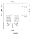
As shown in FIGS. 2A-2E, method 100 utilizes a conventionally formed single-crystal silicon semiconductor wafer 210 that has an overlying base dielectric layer 212. Base dielectric layer 212 can represent a dielectric layer that includes no metal structures, or a dielectric layer that includes metal structures, such as the dielectric layer of a metal interconnect structure.
When formed as the dielectric layer of a metal interconnect structure, base dielectric layer 212 includes levels of metal traces, which are typically aluminum, a large number of contacts that connect the bottom metal trace to electrically conductive regions on wafer 210, and a large number of inter-metal vias that connect the metal traces in adjacent layers together. Further, selected regions on the top surfaces of the metal traces in the top metal layer function as pads which provide external connection points.
In the present example, base dielectric layer 212 represents the dielectric layer of a metal interconnect structure that also includes pads P1-P4. Pads P1 and P2 are selected regions on the top surfaces of two of the metal traces in the top layer of metal traces that provide electrical connections for a to-be-formed coil, while pads P3 and P4 are selected regions on the top surfaces of the metal traces that provide electrical input/output connections for a to-be-formed switch. (Only pads P1-P4, and not the entire metal interconnect structure, are shown in cross-section for clarity.)
Referring again to FIGS. 2A-2E, method 100 begins by forming a metal layer 214 on the top surface of base dielectric layer 212. In the present example, since base dielectric layer 212 represents the dielectric layer of a metal interconnect structure, metal layer 214 is also formed on the top surfaces of the pads P1-P4.
Metal layer 214 can include, for example, a layer of titanium (e.g., 100 Å thick), a layer of titanium nitride (e.g., 200 Å thick), a layer of aluminum copper (e.g., 1.2 μm thick), a layer of titanium (e.g., 44 Å thick), and a layer of titanium nitride (e.g., 250 Å thick). Once metal layer 214 has been formed, a lower mask 216 is formed and patterned on the top surface of metal layer 214.
As shown in FIGS. 3A-3E, following the formation and patterning of mask 216, metal layer 214 is etched to remove the exposed regions of metal layer 214 and form a number of spaced-apart lower coil members 220. The lower coil members 220, which have a horseshoe shape, form the lower sides of the to-be-formed coil. Since base dielectric layer 212 represents the dielectric layer of a metal interconnect structure in the present example, the ends of the lower coil members 220 that correspond with the opposite ends of the to-be-formed coil are physically and electrically connected to pads P1 and P2.
In addition, the etch can optionally form a pair of lower input/output members 222 that are physically and electrically connected to the input/output pads P3 and P4. After the lower coil members 220 and the pair of lower input/output members 222 have been formed, mask 216 is removed.
Returning to FIG. 1, once the lower coil members and the pair of lower input/output members have been formed, method 100 moves to 112 to form a lower dielectric layer that touches the lower coil members and the pair of input/output members. FIGS. 4A, 4B, 4C, 4D, and 4E show a series of views that illustrate an example of method 100 forming a lower dielectric layer in accordance with the present invention.
As shown in FIGS. 4A-4E, a lower dielectric layer 224, such as an oxide layer, is formed on base dielectric layer 212, the lower coil members 220, and the pair of lower input/output members 222. For example, lower dielectric layer can be formed by depositing an oxide, and then chemically-mechanically polishing the oxide to have, for example, a target thickness of, for example, 2000 Å, over base dielectric layer 212.
Referring back to FIG. 1, after the lower dielectric layer has been formed, method 100 moves to 114 to form a sacrificial structure that touches the lower dielectric layer. FIGS. 5A-6A, 5B-6B, 5C-6C, 5D-6D, and 5E-6E show a series of views that illustrate an example of method 100 forming a sacrificial structure in accordance with the present invention.
As shown in FIGS. 5A-5E, once lower dielectric layer 224 has been formed, a sacrificial layer 226 is formed on the top surface of lower dielectric layer 224. For example, a layer of amorphous silicon that has a thickness of, for example, 2000 Å, can be formed on the top surface of lower dielectric layer 224. Once sacrificial layer 226 has been formed, a mask 228 is formed and patterned on the top surface of sacrificial layer 226.
As shown in FIGS. 6A-6E, following the formation and patterning of mask 228, sacrificial layer 226 is etched to remove the exposed regions of sacrificial layer 226 and form a sacrificial structure 230. After sacrificial layer 226 has been etched to form sacrificial structure 230, mask 228 is removed.
Referring again to FIG. 1, after the sacrificial structure has been formed, method 100 moves to 116 to form a core, a switch member, and a suspension member that touch the lower dielectric layer. No portion of the switch member touches the core. FIGS. 7A-9A, 7B-9B, 7C-9C, 7D-9D, and 7E-9E show a series of views that illustrate an example of method 100 forming a core, a switch member, and a suspension member in accordance with the present invention.
As shown in FIGS. 7A-7E, after the formation of sacrificial structure 230, a seed layer 232 is formed on the top surface of lower dielectric layer 224 and sacrificial structure 230. For example, seed layer can be formed by depositing 300 Å of titanium, 3000 Å of copper, and 300 Å of titanium. After seed layer 232 has been formed, a plating mold 234 (shown cross-hatched) is formed and patterned on the top surface of seed layer 232.
Next, following the formation of plating mold 234, as illustrated in FIGS. 8A-8E, the top titanium layer is stripped and a magnetic material, such as an alloy of nickel and iron like permalloy, is deposited by electroplating to a thickness of, for example, 10 μm, to form a core 236, a switch member 238, and a suspension member 240.
After this, plating mold 234 is removed, followed by the removal of the underlying regions of seed layer 232. As shown in FIGS. 9A-9E, core 236, which mirrors the shape of the to-be-formed coil, also has a horseshoe shape that lies over the lower coil members 220, while switch member 238 has a contact sidewall 244.
As further shown in FIGS. 9A-9E, suspension member 240 has an intermediate member 246. Intermediate member 246 lies between core 236 and switch member 238, and lies adjacent to the contact sidewall 244 of switch member 238. As a result, intermediate member 246 is separated from core 236 by an actuation gap 250, while intermediate member 246 is separated from the contact sidewall 244 of switch member 238 by a contact gap 252.
Actuation gap 250 can be made to be slightly larger than contact gap 252, thereby ensuring that an electrical connection will always be made when the relay is activated. The sizes of actuation gap 250 and contact gap 252 are defined by the pattern in plating mold 234. Further, in the present example, intermediate member 246 is also formed to have a half-circle shape, and is oriented towards core 236 to form a racetrack shape. Suspension member 240 also includes a spring member 254. In the present example, as shown in FIGS. 9A-9E, spring member 254 is implemented with a base section 256, which provides the only point where suspension member 240 touches lower dielectric layer 224, and an extension section 260 that, along with intermediate member 246, are spaced apart from dielectric layer 224.
Referring again to FIG. 1, after the core, the switch member, and the suspension member have been formed, method 100 moves to 118 to form tops and sides that touch the lower coil members to form a coil, a conductive first switch trace that sits over the switch member, and a conductive second switch trace that sits over and rides on the suspension member. No portion of the coil is wrapped around the suspension member.
FIGS. 10A-14A, 10B-14B, 10C-14C, 10D-14D, and 10E-14E show a series of views that illustrate an example of method 100 forming tops and sides that touch the lower coil members to form a coil, a conductive first switch trace that sits over the switch member, and a conductive second switch trace that sits over and rides on the suspension member in accordance with the present invention.
As shown in FIGS. 10A-10E, after the formation of core 236, switch member 238, and suspension member 240 have been formed, and after the removal of plating mold 234 and the underlying regions of seed layer 232, an upper dielectric layer 262, such as an oxide layer, is formed on lower dielectric layer 224, core 236, switch member 238, and suspension member 240. For example, upper dielectric layer 262 can be formed by conformally depositing an oxide to a thickness of, for example, 1 μm, over lower dielectric layer 224. After upper dielectric layer 262 has been formed, a mask 264, such as a layer of photoresist, is then formed and patterned on the top surface of upper dielectric layer 262.
Following the formation and patterning of mask 264, as shown in FIGS. 11A-11E, the exposed regions of the upper dielectric layer 262 and underlying lower dielectric layer 224 are etched to form a number of vertical openings 266. The vertical openings 266 include via-type openings that expose the top surfaces of the ends of the lower coil members 220 that form the lower sides of the to-be-formed coil. The vertical openings 266 also expose the pair of lower input/output members 222. In addition, the vertical openings 266 also form a trench that extends from base section 256 around suspension member 240 and back again to base section 256.
In accordance with the present invention, the exposed regions of sacrificial structure 230 are not to be removed during this etch. As a result, vertical openings 266 are formed with an etchant that is highly selective to the material used to form sacrificial structure 230. In addition, sacrificial structure 230, which was formed to have the same thickness as lower dielectric layer 224, can also be formed to be thicker than lower dielectric layer 224 to ensure that a significant portion of the exposed regions of sacrificial structure 230 remain after the etch. Following the etch, mask 264 is then removed.
Once mask 264 has been removed, as shown in FIGS. 12A-12E, a seed layer 270 is formed on the exposed ends of the lower coil members 220, the exposed input/output members 222, lower dielectric layer 224, sacrificial structure 230, and the top surface of upper dielectric layer 262. For example, seed layer can be formed by depositing 300 Å of titanium, 3000 Å of copper, and 300 Å of titanium. After seed layer 270 has been formed, a plating mold 272 (shown cross-hatched) is formed and patterned on the top surface of seed layer 270. The pattern in plating mold 272 is shown hatched in FIG. 12A.
Next, as shown in FIGS. 13A-13E, following the formation and patterning of plating mold 272, the top titanium layer is stripped and copper is deposited by electroplating to form a number of copper side sections 274 of the coil, and a number of copper upper sections 276 of the coil. In addition, the electroplating also forms a first switch trace 280 with a sidewall contact 282, and a second switch trace 284 with a sidewall contact 286. The first and second switch traces 280 and 284 also touch the input/output members 222 to make an electrical connection. As further shown in FIGS. 13A-13E, lower coil member 220-1, side section 274-1, and upper section 276-1 form three sides of one coil loop. Following this, as shown in FIGS. 14A-14E, plating mold 272 and the underlying regions of seed layer 270 are removed.
Referring again to FIG. 1, after the coil, the conductive first switch trace, and the conductive second switch trace have been formed, method 100 moves to 120 to remove the sacrificial structure so that the suspension member moves in response to changes in a current flowing through the coil.
In other words, the conductive second switch trace makes and breaks electrical contact with the first conductive switch trace as the suspension member moves in response to changes in a current flowing through the coil. In addition, a magnetic flux passes through a portion of the suspension member and substantially no magnetic flux passes through the first and the second conductive switch traces when a current flows through the coil.
FIGS. 15A-15E show a series of views that illustrate an example of method 100 removing sacrificial structure 230 in accordance with the present invention. As shown in FIGS. 15A-15E, after the coil, first switch trace 280, and second switch trace 284 have been formed, sacrificial structure 230 is removed. The removal of sacrificial structure 230 leaves intermediate member 246 and extension section 260 of spring member 254 floating. For example, in the example shown in FIGS. 15A-15E, intermediate member 246 and extension section 260 each float, connected to lower dielectric layer 224 only via base section 256.
Floating extension section 260 was vertically spaced apart from lower dielectric layer 224 by underlying sacrificial structure 230, and thereby floats after underlying sacrificial structure 230 has been removed. As a result, the thickness of sacrificial structure 230 determines an offset gap 290, which is the vertical spacing that lies between lower dielectric layer 224 and floating extension section 260.
Thus, as shown in FIGS. 15A-15E, the method of the present invention forms a MEMS relay 1500 that includes core 236 and a coil 1510 that is wrapped around core 236. Coil 1510 can be implemented with the lower coil members 220, the copper side sections 274, and the copper upper sections 276. In addition, both core 236 and coil 1510 touch lower dielectric layer 224.
As further shown in FIGS. 15A-15E, MEMS relay 1500 also includes a switch structure 1512 and a suspension structure 1514. Switch structure 1512 can be implemented with switch member 238, which touches lower dielectric layer 224, and upper dielectric layer 262. Suspension structure 1514 can be implemented with suspension member 240, which touches lower dielectric layer 224, and upper dielectric layer 262. Further, no portion of coil 1510 is wrapped around suspension structure 1514.
As additionally shown in FIGS. 15A-15E, MEMS relay 1500 includes first switch trace 280 that touches and extends along switch structure 1512, and second switch trace 284 that touches and extends along suspension structure 1514. Further, first switch trace 280 has a first sidewall contact 282, and second switch trace 284 has a second sidewall contact 286.
In operation, when no current is present in coil 1510, suspension structure 1514 lies in a rest position as shown in FIG. 15A. In addition, suspension structure 1514 and core 236 are spaced apart by a minimum distance X when no current is present in coil 1510, while first sidewall contact 282 and second sidewall contact 286 are spaced apart by a minimum distance Y when no current is present in coil 1510 that is equal to or less than the minimum distance X. The minimum distance Y, in turn, provides a high-impedance electrical pathway.
Thus, one of the advantages of MEMS relay 1500 is that suspension structure 1514 is independent of core 236 (i.e., no portion of suspension structure 1514 touches core 236 when no current flows through coil 1510). Thus, the suspension structure 1514 can be optimized to reduce the stiffness of the spring while core 236 can be optimized for a short flux path.
On the other hand, when a current flows through coil 1510 and generates an electromagnetic field that is stronger than the spring force of suspension structure 1514, suspension structure 1514 moves towards core 236 so that the first and second sidewall contacts 282 and 286 touch, thereby providing a low-impedance electrical pathway.
Thus, the second sidewall contact 286 of second switch trace 284 moves towards and touches the first sidewall contact 282 of first switch trace 280 when a current flows through coil 1510, and moves away from the first sidewall contact 282 of first switch trace 280 when no current flows through coil 1510. Thus, no portion of suspension structure 1514 touches core 236 when no current flows through coil 1510.
Further, as shown in FIG. 15A, in accordance with the present invention, a magnetic flux 1516 passes through a portion of suspension member 240 when a current flows through coil 1510, while and substantially no magnetic flux passes through the first and the second switch traces 280 and 284 when a current flows through coil 1510. Thus, one of the advantages of the present invention is that MEMS relay 1500 is insensitive to fluctuations in the current around the core and, thereby the flux. As a result, signals with very small amplitudes can pass through relay 1500 with no flux-based distortion.
Thus, a method of forming a MEMS relay in accordance with the present invention has been described. The elements shown in FIG. 1 can be implemented in a number of different ways. For example, the spaced-apart lower coil members that form the lower horizontal sections of the coil described in element 110 of FIG. 1 can be alternately formed.
FIGS. 16A-18A, 16B-18B, 16C-18C, 16D-18D, and 16E-18E show a series of views that illustrate a first example of an alternate way of implementing element 110 of method 100, which forms a number of spaced-apart lower coil members of the to-be-formed coil, in accordance with the present invention.
As with the example shown in FIGS. 2A-3E, the example shown in FIGS. 16A-18E also utilizes single-crystal silicon semiconductor wafer 210 with overlying base dielectric layer 212. The FIGS. 16A-18E example begins by forming a seed layer 1610 on base dielectric layer 212 and the pads P1-P4 which are exposed via openings in base dielectric layer 212.
Once seed layer 1610 has been formed, a plating mold 1612 is formed on the top surface of seed layer 1610. As shown in FIGS. 17A-17E, following the formation of plating mold 1612, copper is deposited by electroplating to form the number of spaced-apart lower coil members 220 and the pair of lower input/output members 222.
As shown in FIGS. 18A-18E, after the lower coil members 220 and the pair of lower input/output members 222 have been formed, plating mold 1612 is removed, followed by the removal of the underlying regions of seed layer 1610. As shown, the structure illustrated in FIGS. 18A-18E is similar to the structure shown in FIGS. 3A-3E.
FIGS. 19A-21A, 19B-21B, 19C-21C, 19D-21D, and 19E-21E show a series of views that illustrate a second example of an alternate way of implementing element 110 of method 100, which forms a number of spaced-apart lower coil members of the to-be-formed coil, in accordance with the present invention.
As with the example shown in FIGS. 2A-3E, the example shown in FIGS. 19A-21E also utilizes single-crystal silicon semiconductor wafer 210 with overlying base dielectric layer 212. The FIGS. 19A-21E example begins by forming a mask 1910 on the top surface of base dielectric layer 212. Following this, the exposed regions of base dielectric layer 212 are etched to form a number of spaced-apart trenches 1912, which will define the spaced-apart lower coil members of the to-be-formed coil, in the top surface of base dielectric layer 212. One of the trenches 1912 exposes pad P1, while another of the trenches 1912 exposes pad P2. In addition, the etch also forms a pair of openings 1914 in base dielectric layer 212 that expose the pair of pads P3 and P4.
Following the etch, as shown in FIGS. 20A-20E, with mask 1910 in place, a copper structure 1916 is formed in the trenches 1912 and the openings 1914 on the exposed regions of base dielectric layer 212, pads P1-P4, and mask 1910. Copper structure 1916 can be formed by, for example, evaporating, in sequence, 300 Å of titanium, 1 μm copper, and 300 Å of titanium.
Next, as shown in FIGS. 21A-21E, after copper structure 1916 has been formed, mask 1910 is stripped which, in turn, lifts off the overlying layer of copper structure 1916. The removal of mask 1910 leaves the copper structure 1916 only on base dielectric layer 212, thereby forming the number of spaced-apart lower coil members 220 and the pair of lower input/output members 222. As shown, other than being recessed, the structure illustrated in FIGS. 21A-21E is similar to the structure shown in FIGS. 3A-3E.
FIGS. 22A-26A, 22B-26B, 22C-26C, 22D-26D, and 22E-26E show a series of views that illustrate an example of an alternate way of implementing element 118 of method 100, which forms the tops and the sides of the to-be-formed coil and the traces for the switch, in accordance with the present invention.
The FIGS. 22A-26E example is the same as the FIGS. 2A-15E example up through the formation of seed layer 270, and differs by forming a plating mold 2210 on the top surface of seed layer 270 in lieu of plating mold 272. Plating mold 2210 differs from plating mold 272 in that plating mold 2210 prevents the first and second sidewall contacts 282 and 286 from being formed from the to-be-formed copper. The pattern in mold 2210 is shown hatched in FIG. 22A.
Next, following the formation of mold 2210, copper is deposited by electroplating to form the number of copper side sections 274 of the coil, and the number of copper upper sections 276 of the coil. In addition, the electroplating also forms a first switch trace 2212, which is the same as switch trace 280 except that there is no sidewall contact 282, and a second switch trace 2214, which is the same as switch trace 284 except that there is no sidewall contact 286. Following this, as shown in FIGS. 23A-23E, mold 2210 and the underlying regions of seed layer 270 are removed.
Following this, as shown in FIGS. 24A-24E, a mask 2216 is formed and patterned on upper dielectric layer 262, the copper upper sections 276, first switch trace 2212, and second switch trace 2214. Once mask 2216 has been formed and patterned, a conductive layer 2220, such as a layer of titanium, nickel, or chrome, and an overlying layer of gold, is deposited on the exposed regions of upper dielectric layer 262 that surround switch member 238, the exposed regions of upper dielectric layer 262 that surround suspension member 240, the exposed regions of sacrificial structure 230, and mask 2216. When sputtered, titanium, nickel, chrome, and gold provide good coverage on the high-aspect ratio (vertical) sidewalls of the switch member 238 and suspension member 240 that face each other. Titanium, nickel, and chrome, in turn, improve the adhesion of gold.
As shown in FIGS. 25A-25E, after conductive layer 2220 has been formed, mask 2216 is stripped which, in turn, lifts off the overlying layer of conductive layer 2220. The removal of mask 2216 leaves the conductive layer 2220 on the sidewalls of upper dielectric layer 262 over switch member 238 and first switch trace 2212, and the sidewalls of upper dielectric layer 262 over suspension member 240 and second switch trace 2214, thereby forming a sidewall contact 2222 of first switch trace 2212 and a sidewall contact of 2224 of second switch trace 2214 that faces sidewall contact 2222.
Following this, as shown in FIGS. 26A-26E, sacrificial structure 230 is removed. The removal of sacrificial structure 230 leaves intermediate member 246 and extension section 260 of spring member 254 floating as before, but with gold contacts.
In addition to the above, the structures can be formed to have different shapes. For example, mask 228 can be formed to have different shapes so that sacrificial structure 230 has different shapes. In addition, plating mold 234 can be formed to have different shapes that correspond with the shapes of sacrificial structure 230 so that core 236, switch member 238, and suspension member 240 have different shapes.
For example, FIGS. 27A-27E show a series of views that illustrate an example of sacrificial structure 230 and spring member 254 with a different shape in accordance with the present invention. In the FIGS. 27A-27E example, spring member 254 is formed with a pair of facing structures that each include a base section 256 and a C-shaped extension section 260.
Further, FIGS. 28A-28E show a series of views that illustrate an example of sacrificial structure 230, core 236, intermediate member 246, and spring member 254 with a different shape in accordance with the present invention. In the FIGS. 28A-28E example, core 236 is formed as a nearly complete doughnut shape, while intermediate member 246 is formed with a wedge or pie shape that fits into the opening in the nearly complete doughnut shape. In addition, spring member 254 is also formed with a pair of facing structures that each include base section 256 and a C-shaped section 260.
As noted above, dielectric layer 212 can represent a dielectric layer that is free of metal structures. When free of metal structures, the electrical connections to coil 1510 can be made, for example, by wire bonding to points on the copper upper sections 276 that represent opposite ends of coil 1510. In addition, connections to the first and second switch traces 280 and 284 can be made, for example, by wire bonding. Another of the advantages of the present invention is that the present invention requires relatively low processing temperatures. As a result, the present invention is compatible with conventional backend CMOS processes.
It should be understood that the above descriptions are examples of the present invention, and that various alternatives of the invention described herein may be employed in practicing the invention. For example, the various seed layers can be implemented as copper seed layers, or as tungsten, chrome, or combination seed layers as need to provide the correct ohmic and mechanical (peel) characteristics. In addition, a double throw switch can be easily fabricated by using two MEMS relays 1500 which are positioned as mirror images of each other. Thus, it is intended that the following claims define the scope of the invention and that structures and methods within the scope of these claims and their equivalents be covered thereby.

Claims (20)

1. A microelectromechanical system (MEMS) structure comprising:
a semiconductor body having a non-conductive top surface;
a coil having a plurality of coil segments that touch the non-conductive top surface;
a dielectric structure touching the plurality of coil segments and the non-conductive top surface;
a plurality of structures, the plurality of structures including:
a first magnetic member touching the dielectric structure, the first magnetic member lying directly vertically above the plurality of coil segments;
a second magnetic member touching the dielectric structure, the second magnetic member being completely spaced apart from the first magnetic member when no current flows in the coil, and moving towards the first magnetic member in response to a current flowing in the coil;
a stationary structure touching the dielectric structure and having a first conductive member;
a non-conductive region touching the second magnetic member; and
a second conductive member touching the non-conductive region, lying directly vertically above the second magnetic member, being completely spaced apart from the first conductive member when the second magnetic member is spaced apart from the first magnetic member, and moving towards and making an electrical connection to the first conductive member when the second magnetic member moves towards the first magnetic member.
2. The MEMS structure of claim 1 wherein when the second conductive member makes an electrical connection to the first conductive member, only a first surface region of the first conductive member physically touches the second conductive member and only a second surface region of the second conductive member physically touches the first conductive member, the second surface region moving substantially only in a horizontal direction towards the first surface region when the second magnetic member moves towards the first magnetic member.
3. The MEMS structure of claim 1 wherein when the second conductive member makes an electrical connection to the first conductive member, only a first surface region of the first conductive member physically touches the second conductive member and only a second surface region of the second conductive member physically touches the first conductive member, the first surface region being substantially vertical, the second surface region being substantially vertical.
4. The MEMS structure of claim 1 wherein no portion of the second conductive member is electrically connected to the second magnetic member.
5. The MEMS structure of claim 1 wherein none of the plurality of coil segments lie directly vertically below any portion of the second magnetic member.
6. The MEMS structure of claim 1 wherein the first magnetic member lies between a first portion of the second magnetic member and a second portion of the second magnetic member.
7. A method of forming a microelectromechanical system (MEMS) structure on a semiconductor body having a non-conductive top surface comprising:
forming a coil having a plurality of coil segments that touch the non-conductive top surface;
forming a dielectric structure to touch the plurality of coil segments and the non-conductive top surface;
forming a plurality of structures, the plurality of structures including:
a first magnetic member touching the dielectric structure, the first magnetic member lying directly vertically above the plurality of coil segments;
a second magnetic member touching the dielectric structure, the second magnetic member being completely spaced apart from the first magnetic member when no current flows in the coil, and moving towards the first magnetic member in response to a current flowing in the coil;
a stationary structure touching the dielectric structure and having a first conductive member;
a non-conductive region touching the second magnetic member; and
a second conductive member touching the non-conductive region, lying directly vertically above the second magnetic member, being completely spaced apart from the first conductive member when the second magnetic member is spaced apart from the first magnetic member, and moving towards and making an electrical connection to the first conductive member when the second magnetic member moves towards the first magnetic member.
8. The method of claim 7 wherein forming the plurality of structures includes:
forming a sacrificial layer that touches the dielectric structure; and
etching the sacrificial layer to form a sacrificial region that touches the dielectric structure.
9. The method of claim 8 wherein forming the plurality of structures further includes:
forming a seed layer that touches the dielectric structure and the sacrificial region;
forming a mold that touches the seed layer, the mold having a first opening that exposes a region of the seed layer that lies above the dielectric structure and the plurality of coil segments, a second opening spaced apart from the first opening that exposes a region of the seed layer that lies above the dielectric structure and the sacrificial region, and a third opening spaced apart from the first and second openings that exposes a region of the seed layer that lies above the dielectric structure; and
forming a magnetic material in the mold to form the first magnetic member in the first opening, the second magnetic member in the second opening, and a third magnetic member in the third opening.
10. The method of claim 9 wherein forming the plurality of structures further includes:
forming a non-conductive layer to touch the first, second, and third magnetic members;
forming a sacrificial opening through the non-conductive layer to expose the sacrificial region;
forming a layer of seed material that touches the non-conductive layer and the sacrificial region exposed by the sacrificial opening;
forming a mold structure that touches the layer of seed material, the mold structure having a first opening that exposes a region of the seed layer that lies above the third magnetic member, and a second opening that exposes a region of the seed layer that lies above the second magnetic member;
forming a conductive material in the mold structure to form the first conductive member in the first opening of the mold structure, and the second conductive member in the second opening of the mold structure; and
removing the sacrificial region from below the second magnetic member.
11. The method of claim 10 wherein the stationary structure includes the third magnetic member and a portion of the non-conductive layer.
12. The method of claim 10 wherein forming the plurality of structures further includes:
forming a plurality of coil openings in the non-conductive layer and the dielectric structure to expose a plurality of portions of the plurality of coil segments simultaneously with forming the sacrificial opening;
forming the layer of seed material to touch the plurality of portions of the plurality of coil segments exposed by the plurality of coil openings simultaneously with forming the layer of seed material to touch the sacrificial region exposed by the sacrificial opening;
forming the mold structure to have a plurality of coil openings simultaneously with forming the first opening of the mold structure, and the second opening of the mold structure; and
forming the conductive material in the mold structure to form a plurality of coil sections in the plurality of coil openings simultaneously with forming the conductive material in the first and second openings of the mold structure, the plurality of coil sections touching the plurality of coil segments to form the coil.
13. The method of claim 10 wherein forming the plurality of structures further includes:
forming a seed material layer that touches the first conductive member and the second conductive member;
forming a mold layer that touches the seed material layer, the mold layer having a first opening that exposes a side wall of the first conductive member, and a second opening that exposes a side wall of the second conductive member;
forming a conductive material in the first opening and the second opening of the mold layer to form a first conductive contact that touches the side wall of the first conductive member, and a second conductive contact that touches a side wall of the second conductive member; and
removing the mold layer, an air gap lying between the first contact and the second contact, the first contact facing the second contact, the sacrificial region being removed after the mold layer is removed.
14. The method of claim 7 wherein forming the plurality of coil segments of the coil includes:
forming a layer of conductive material to touch the non-conductive top surface; and
etching the layer of conductive material to form the plurality of coil segments.
15. The method of claim 7 wherein forming the plurality of coil segments of the coil includes:
forming a layer of seed material to touch the non-conductive top surface;
forming a mold structure to touch the layer of seed material; and
forming a conductive material in the mold structure to form the plurality of coil segments.
16. The method of claim 7 wherein forming the plurality of coil segments of the coil includes:
etching the non-conductive top surface to expose a plurality of spaced apart conductive regions;
forming a layer of conductive material to touch the non-conductive top surface and the plurality of conductive regions; and
planarizing the layer of conductive material to form the plurality of coil segments.
17. A microelectromechanical system (MEMS) structure comprising:
a semiconductor body having a non-conductive top surface;
a coil having a plurality of coil segments that touch the non-conductive top surface;
a dielectric structure touching the plurality of coil segments and the non-conductive top surface;
a plurality of structures, the plurality of structures including:
a first magnetic member touching the dielectric structure, the first magnetic member lying directly vertically above the plurality of coil segments;
a second magnetic member touching the dielectric structure, the second magnetic member being completely spaced apart from the first magnetic member when no current flows in the coil, and moving towards the first magnetic member in response to a current flowing in the coil;
a plurality of pads that touch the non-conductive top surface, the plurality of pads being conductive, lying substantially in a single horizontal plane, and including a first pad, a second pad, and a third pad, the third pad lying directly vertically below a coil segment of the plurality of coil segments;
a stationary structure touching the dielectric structure and having a first conductive member, the first conductive member being permanently electrically connected to the first pad;
a non-conductive region touching the second magnetic member; and
a second conductive member touching the non-conductive region, being permanently electrically connected to the second pad, being completely spaced apart from the first conductive member when the second magnetic member is spaced apart from the first magnetic member, and moving towards and making an electrical connection to the first conductive member when the second magnetic member moves towards the first magnetic member.
18. The MEMS structure of claim 17 wherein the plurality of pads are spaced apart from the dielectric structure.
19. The MEMS structure of claim 17 wherein:
no portion of the second conductive member is electrically connected to the second magnetic member; and
no portion of the coil is wrapped around any portion of the second magnetic member.
20. The MEMS structure of claim 17 wherein the first magnetic member lies between a first portion of the second magnetic member and a second portion of the second magnetic member.
US12/218,368 2008-07-11 2008-07-11 MEMS relay with a flux path that is decoupled from an electrical path through the switch and a suspension structure that is independent of the core structure and a method of forming the same Active 2028-09-29 US7902946B2 (en)

Priority Applications (6)

Application Number Priority Date Filing Date Title
US12/218,368 US7902946B2 (en) 2008-07-11 2008-07-11 MEMS relay with a flux path that is decoupled from an electrical path through the switch and a suspension structure that is independent of the core structure and a method of forming the same
TW098122170A TWI492259B (en) 2008-07-11 2009-07-01 Mems relay with a flux path that is decoupled from an electrical path through the switch and a suspension structure that is independent of the core structure and a method of forming the same
PCT/US2009/049675 WO2010005888A2 (en) 2008-07-11 2009-07-06 Mems relay
KR1020107023829A KR101724717B1 (en) 2008-07-11 2009-07-06 Mems relay
DE112009001086T DE112009001086T5 (en) 2008-07-11 2009-07-06 Microsystem relay
JP2011517499A JP5456777B2 (en) 2008-07-11 2009-07-06 MEMS relay

Applications Claiming Priority (1)

Application Number Priority Date Filing Date Title
US12/218,368 US7902946B2 (en) 2008-07-11 2008-07-11 MEMS relay with a flux path that is decoupled from an electrical path through the switch and a suspension structure that is independent of the core structure and a method of forming the same

Publications (2)

Publication Number Publication Date
US20100007448A1 US20100007448A1 (en) 2010-01-14
US7902946B2 true US7902946B2 (en) 2011-03-08

Family

ID=41504642

Family Applications (1)

Application Number Title Priority Date Filing Date
US12/218,368 Active 2028-09-29 US7902946B2 (en) 2008-07-11 2008-07-11 MEMS relay with a flux path that is decoupled from an electrical path through the switch and a suspension structure that is independent of the core structure and a method of forming the same

Country Status (6)

Country Link
US (1) US7902946B2 (en)
JP (1) JP5456777B2 (en)
KR (1) KR101724717B1 (en)
DE (1) DE112009001086T5 (en)
TW (1) TWI492259B (en)
WO (1) WO2010005888A2 (en)

Cited By (5)

* Cited by examiner, † Cited by third party
Publication number Priority date Publication date Assignee Title
US20100171577A1 (en) * 2008-03-20 2010-07-08 Todd Richard Christenson Integrated Microminiature Relay
US20110140814A1 (en) * 2005-03-04 2011-06-16 Ht Microanalytical, Inc. Miniaturized Switch Device
US8378766B2 (en) 2011-02-03 2013-02-19 National Semiconductor Corporation MEMS relay and method of forming the MEMS relay
US20140008559A1 (en) * 2011-02-03 2014-01-09 UT-Battelle. LLC Mesofluidic digital valve
US9284183B2 (en) 2005-03-04 2016-03-15 Ht Microanalytical, Inc. Method for forming normally closed micromechanical device comprising a laterally movable element

Families Citing this family (3)

* Cited by examiner, † Cited by third party
Publication number Priority date Publication date Assignee Title
JP2013068757A (en) * 2011-09-22 2013-04-18 Japan Display East Co Ltd Display device
CN107748826B (en) * 2017-11-08 2018-09-25 哈尔滨工业大学 A kind of resistance to mechanical property storage degradation analysis method of relay
JP6950613B2 (en) 2018-04-11 2021-10-13 Tdk株式会社 Magnetically actuated MEMS switch

Citations (23)

* Cited by examiner, † Cited by third party
Publication number Priority date Publication date Assignee Title
US5578976A (en) 1995-06-22 1996-11-26 Rockwell International Corporation Micro electromechanical RF switch
US5880921A (en) 1997-04-28 1999-03-09 Rockwell Science Center, Llc Monolithically integrated switched capacitor bank using micro electro mechanical system (MEMS) technology
US6016092A (en) 1997-08-22 2000-01-18 Qiu; Cindy Xing Miniature electromagnetic microwave switches and switch arrays
US6094116A (en) 1996-08-01 2000-07-25 California Institute Of Technology Micro-electromechanical relays
US6169826B1 (en) 1998-05-12 2001-01-02 Hitachi Metals, Ltd. Optical switch
US6310526B1 (en) * 1999-09-21 2001-10-30 Lap-Sum Yip Double-throw miniature electromagnetic microwave (MEM) switches
US6360036B1 (en) 2000-01-14 2002-03-19 Corning Incorporated MEMS optical switch and method of manufacture
US6469602B2 (en) 1999-09-23 2002-10-22 Arizona State University Electronically switching latching micro-magnetic relay and method of operating same
US20030030998A1 (en) 2001-07-02 2003-02-13 Memscap Microelectromechanical component
US6573822B2 (en) 2001-06-18 2003-06-03 Intel Corporation Tunable inductor using microelectromechanical switches
US20030137374A1 (en) * 2002-01-18 2003-07-24 Meichun Ruan Micro-Magnetic Latching switches with a three-dimensional solenoid coil
US20040001667A1 (en) 2002-06-28 2004-01-01 Childers Winthrop D. Switching apparatus
US20040012469A1 (en) * 2001-12-10 2004-01-22 Hei, Inc. Low voltage MEM switch
US20040022484A1 (en) 2000-01-07 2004-02-05 Susanne Sigloch Fiber-optic switching element
US6803843B2 (en) * 2001-02-22 2004-10-12 Canon Kabushiki Kaisha Movable-body apparatus, optical deflector, and method of fabricating the same
US6842558B2 (en) 2001-11-15 2005-01-11 Seiko Instruments Inc. Optical switch manufacturing method thereof
JP2006210065A (en) 2005-01-26 2006-08-10 Matsushita Electric Works Ltd Microrelay
US7095919B2 (en) 2002-07-12 2006-08-22 Omron Corporation Optical switch
US7202763B2 (en) 2002-09-25 2007-04-10 Nxp B.V. Micro-electromechanical switching device
US7382218B2 (en) * 2002-12-10 2008-06-03 Commissariat A L'energie Atomique Micromechanical switch and production process thereof
US7381663B2 (en) 2003-02-17 2008-06-03 Nippon Telegraph And Telephone Corporation Method of fabricating a surface shape recognition sensor
US7444042B1 (en) 2007-05-25 2008-10-28 National Semiconductor Corporation Optical switch
US7464459B1 (en) 2007-05-25 2008-12-16 National Semiconductor Corporation Method of forming a MEMS actuator and relay with vertical actuation

Family Cites Families (3)

* Cited by examiner, † Cited by third party
Publication number Priority date Publication date Assignee Title
JP3750574B2 (en) * 2001-08-16 2006-03-01 株式会社デンソー Thin film electromagnet and switching element using the same
JP4305293B2 (en) * 2003-10-14 2009-07-29 横河電機株式会社 relay
US7101724B2 (en) * 2004-02-20 2006-09-05 Wireless Mems, Inc. Method of fabricating semiconductor devices employing at least one modulation doped quantum well structure and one or more etch stop layers for accurate contact formation

Patent Citations (25)

* Cited by examiner, † Cited by third party
Publication number Priority date Publication date Assignee Title
US5578976A (en) 1995-06-22 1996-11-26 Rockwell International Corporation Micro electromechanical RF switch
US6094116A (en) 1996-08-01 2000-07-25 California Institute Of Technology Micro-electromechanical relays
US5880921A (en) 1997-04-28 1999-03-09 Rockwell Science Center, Llc Monolithically integrated switched capacitor bank using micro electro mechanical system (MEMS) technology
US6016092A (en) 1997-08-22 2000-01-18 Qiu; Cindy Xing Miniature electromagnetic microwave switches and switch arrays
US6169826B1 (en) 1998-05-12 2001-01-02 Hitachi Metals, Ltd. Optical switch
US6310526B1 (en) * 1999-09-21 2001-10-30 Lap-Sum Yip Double-throw miniature electromagnetic microwave (MEM) switches
US6469602B2 (en) 1999-09-23 2002-10-22 Arizona State University Electronically switching latching micro-magnetic relay and method of operating same
US20040022484A1 (en) 2000-01-07 2004-02-05 Susanne Sigloch Fiber-optic switching element
US6360036B1 (en) 2000-01-14 2002-03-19 Corning Incorporated MEMS optical switch and method of manufacture
US6803843B2 (en) * 2001-02-22 2004-10-12 Canon Kabushiki Kaisha Movable-body apparatus, optical deflector, and method of fabricating the same
US6573822B2 (en) 2001-06-18 2003-06-03 Intel Corporation Tunable inductor using microelectromechanical switches
US20030030998A1 (en) 2001-07-02 2003-02-13 Memscap Microelectromechanical component
US6842558B2 (en) 2001-11-15 2005-01-11 Seiko Instruments Inc. Optical switch manufacturing method thereof
US20040012469A1 (en) * 2001-12-10 2004-01-22 Hei, Inc. Low voltage MEM switch
US20030137374A1 (en) * 2002-01-18 2003-07-24 Meichun Ruan Micro-Magnetic Latching switches with a three-dimensional solenoid coil
US20060049900A1 (en) 2002-01-18 2006-03-09 Magfusion, Inc. Micro-magnetic latching switches with a three-dimensional solenoid coil
US7327211B2 (en) 2002-01-18 2008-02-05 Schneider Electric Industries Sas Micro-magnetic latching switches with a three-dimensional solenoid coil
US20040001667A1 (en) 2002-06-28 2004-01-01 Childers Winthrop D. Switching apparatus
US7095919B2 (en) 2002-07-12 2006-08-22 Omron Corporation Optical switch
US7202763B2 (en) 2002-09-25 2007-04-10 Nxp B.V. Micro-electromechanical switching device
US7382218B2 (en) * 2002-12-10 2008-06-03 Commissariat A L'energie Atomique Micromechanical switch and production process thereof
US7381663B2 (en) 2003-02-17 2008-06-03 Nippon Telegraph And Telephone Corporation Method of fabricating a surface shape recognition sensor
JP2006210065A (en) 2005-01-26 2006-08-10 Matsushita Electric Works Ltd Microrelay
US7444042B1 (en) 2007-05-25 2008-10-28 National Semiconductor Corporation Optical switch
US7464459B1 (en) 2007-05-25 2008-12-16 National Semiconductor Corporation Method of forming a MEMS actuator and relay with vertical actuation

Non-Patent Citations (22)

* Cited by examiner, † Cited by third party
Title
Ernst Thielicke and Ernst Obermeier, "A Fast Switching Surface Micromachined Electrostatic Relay", The 12th International Conference on Solid State Sensors, Actuators and Microsystems, Boston, Jun. 8-12, 2003, pp. 899-902.
Gary D. Gray Jr. and Paul A. Kohl, "Magnetically Bistable Actuator Part 1. Ultra-Low Switching Energy And Modeling", Sensors and Actuators A: Physical, vol. 119, Issue 2, Apr. 13, 2005, pp. 489-501.
Gary D. Gray Jr., et al. "Magnetically Bistable Actuator Part 2. Fabrication and Performance", Sensors and Actuators A: Physical, vol. 119, Issue 2, Apr. 13, 2005, pp. 502-511.
Han S. Lee, et al., "Micro-Electro-Mechanical Relays-Design Concepts and Process Demonstrations", Joint 22nd International Conference on Electrical Contacts and 50th IEEE HOLM Conference on Electrical Contacts, Sep. 20-23, 2004, pp. 242-247.
International Search Report for PCT/US2009/049675 filed on Jul. 6, 2009.
J.H. Fabian, et al., "Matrix Cominbination of MEMS Relays", 17th IEEE International Conference on Micro Electro Mechanical Systems, 2004, pp. 861-864.
John A. Wright, et al., "Magnetostatic MEMS Relays For The Miniaturization Of Brushless DC Motor Controllers", 12th IEEE International Conference on Micro Electro Mechanical Systems, Jan. 17-21, 1999, pp. 594-599.
John A. Wright, et al., "Micro-Miniature Electromagnetic Switches Fabricated Using MEMS Technology", Proceedings: 46th Annual International Relay Conference: NARM '98, Oak Brook, Illinois, Apr. 1998, pp. 13-1 to 13-4.
John A. Wright, et al., "Micro-Miniature Electromagnetic Switches Fabricated Using MEMS Technology," Proceedings: 46th Annual International Relay Conference:NARM '98, Oak Brook, Illinois, Apr. 1998, pp. 13-1 to 13-4.
Ren Wanbin, et al., "Finite Element Analysis of Magnetic Structures for Micro-Electro-Mechanical Relays", Proceedings of the 51st IEEE HOLM Conference on Electrical Contacts, Sep. 26-28, 2005, pp. 265-269.
U.S. Appl. No. 11/805,933, filed May 25, 2007 to Niblock et al.
U.S. Appl. No. 11/805,933, filed May 25, 2007, Niblock et al.
U.S. Appl. No. 11/805,934, filed May 25, 2007 to Niblock et al.
U.S. Appl. No. 11/805,934, filed May 25, 2007, Niblock et al.
U.S. Appl. No. 11/805,955, filed May 25, 2007 to Niblock et al.
U.S. Appl. No. 11/805,955, filed May 25, 2007, Niblock et al.
U.S. Appl. No. 11/807,161, filed May 25, 2007 to Niblock et al.
U.S. Appl. No. 11/807,161, filed May 25, 2007, Niblock et al.
U.S. Appl. No. 11/807,162, filed May 25, 2007 to Niblock et al.
U.S. Appl. No. 11/807,162, filed May 25, 2007, Niblock et al.
U.S. Appl. No. 12/283,969, filed Sep. 17, 2008 to Niblock et al.
Written Opinion of the International Searching Authority for PCT/US2009/049675 filed on Jul. 6, 2009.

Cited By (8)

* Cited by examiner, † Cited by third party
Publication number Priority date Publication date Assignee Title
US20110140814A1 (en) * 2005-03-04 2011-06-16 Ht Microanalytical, Inc. Miniaturized Switch Device
US8258900B2 (en) * 2005-03-04 2012-09-04 Ht Microanalytical, Inc. Miniaturized switch device
US9284183B2 (en) 2005-03-04 2016-03-15 Ht Microanalytical, Inc. Method for forming normally closed micromechanical device comprising a laterally movable element
US20100171577A1 (en) * 2008-03-20 2010-07-08 Todd Richard Christenson Integrated Microminiature Relay
US8665041B2 (en) 2008-03-20 2014-03-04 Ht Microanalytical, Inc. Integrated microminiature relay
US8378766B2 (en) 2011-02-03 2013-02-19 National Semiconductor Corporation MEMS relay and method of forming the MEMS relay
US8446237B1 (en) 2011-02-03 2013-05-21 National Semiconductor Corporation MEMS relay and method of forming the MEMS relay
US20140008559A1 (en) * 2011-02-03 2014-01-09 UT-Battelle. LLC Mesofluidic digital valve

Also Published As

Publication number Publication date
WO2010005888A2 (en) 2010-01-14
WO2010005888A3 (en) 2010-04-15
DE112009001086T5 (en) 2012-01-12
KR20110027649A (en) 2011-03-16
US20100007448A1 (en) 2010-01-14
KR101724717B1 (en) 2017-04-07
JP2011527821A (en) 2011-11-04
JP5456777B2 (en) 2014-04-02
TWI492259B (en) 2015-07-11
TW201007802A (en) 2010-02-16

Similar Documents

Publication Publication Date Title
US7902946B2 (en) MEMS relay with a flux path that is decoupled from an electrical path through the switch and a suspension structure that is independent of the core structure and a method of forming the same
US7464459B1 (en) Method of forming a MEMS actuator and relay with vertical actuation
US8446237B1 (en) MEMS relay and method of forming the MEMS relay
US7064637B2 (en) Recessed electrode for electrostatically actuated structures
US6667245B2 (en) CMOS-compatible MEM switches and method of making
US7545234B2 (en) Microelectromechanical device having a common ground plane layer and a set of contact teeth and method for making aspects thereof
JP2004530253A (en) Monolithic switch
KR100419233B1 (en) MEMS device and a fabrication method thereof
KR100619488B1 (en) Microswitching device and method of manufacturing the same
US6962832B2 (en) Fabrication method for making a planar cantilever, low surface leakage, reproducible and reliable metal dimple contact micro-relay MEMS switch
JP2008511105A (en) Plate-based microelectromechanical switch with relative arrangement of contact structure and support arm
JP2007535797A (en) Beam for micromachine technology (MEMS) switches
US7644490B1 (en) Method of forming a microelectromechanical (MEMS) device
JP5131298B2 (en) Switch, manufacturing method thereof, and electrostatic relay
US20110209970A1 (en) Switch and method for manufacturing the same, and relay
EP1556877B1 (en) A micromachined relay with inorganic insulation
EP2365499A1 (en) Switch and method for manufacturing the same, and relay
US7602267B1 (en) MEMS actuator and relay with horizontal actuation
US20060109069A1 (en) Planarized structure for a reliable metal-to-metal contact micro-relay mems switch
US7598829B1 (en) MEMS actuator and relay with vertical actuation
CN105712285A (en) Mems Structure With Multilayer Membrane
EP3038126A1 (en) MEMS structure with thick movable membrane
JP2016177991A (en) Method of manufacturing magnetic lead switch
JP2016207262A (en) Magnetic lead switch
JP2016177990A (en) Magnetic lead switch

Legal Events

Date Code Title Description
AS Assignment

Owner name: NATIONAL SEMICONDUCTOR CORPORATION, CALIFORNIA

Free format text: ASSIGNMENT OF ASSIGNORS INTEREST;ASSIGNOR:NIBLOCK, TREVOR;REEL/FRAME:021293/0240

Effective date: 20080711

STCF Information on status: patent grant

Free format text: PATENTED CASE

FPAY Fee payment

Year of fee payment: 4

MAFP Maintenance fee payment

Free format text: PAYMENT OF MAINTENANCE FEE, 8TH YEAR, LARGE ENTITY (ORIGINAL EVENT CODE: M1552); ENTITY STATUS OF PATENT OWNER: LARGE ENTITY

Year of fee payment: 8

MAFP Maintenance fee payment

Free format text: PAYMENT OF MAINTENANCE FEE, 12TH YEAR, LARGE ENTITY (ORIGINAL EVENT CODE: M1553); ENTITY STATUS OF PATENT OWNER: LARGE ENTITY

Year of fee payment: 12