US7882299B2 - System and method for use of on-chip non-volatile memory write cache - Google Patents
System and method for use of on-chip non-volatile memory write cache Download PDFInfo
- Publication number
- US7882299B2 US7882299B2 US11/021,200 US2120004A US7882299B2 US 7882299 B2 US7882299 B2 US 7882299B2 US 2120004 A US2120004 A US 2120004A US 7882299 B2 US7882299 B2 US 7882299B2
- Authority
- US
- United States
- Prior art keywords
- data
- memory
- volatile memory
- array
- addressable
- Prior art date
- Legal status (The legal status is an assumption and is not a legal conclusion. Google has not performed a legal analysis and makes no representation as to the accuracy of the status listed.)
- Active, expires
Links
Images


Classifications
-
- G—PHYSICS
- G11—INFORMATION STORAGE
- G11C—STATIC STORES
- G11C16/00—Erasable programmable read-only memories
- G11C16/02—Erasable programmable read-only memories electrically programmable
- G11C16/06—Auxiliary circuits, e.g. for writing into memory
- G11C16/10—Programming or data input circuits
- G11C16/12—Programming voltage switching circuits
-
- G—PHYSICS
- G06—COMPUTING OR CALCULATING; COUNTING
- G06F—ELECTRIC DIGITAL DATA PROCESSING
- G06F12/00—Accessing, addressing or allocating within memory systems or architectures
- G06F12/02—Addressing or allocation; Relocation
- G06F12/08—Addressing or allocation; Relocation in hierarchically structured memory systems, e.g. virtual memory systems
- G06F12/0802—Addressing of a memory level in which the access to the desired data or data block requires associative addressing means, e.g. caches
- G06F12/0893—Caches characterised by their organisation or structure
-
- G—PHYSICS
- G06—COMPUTING OR CALCULATING; COUNTING
- G06F—ELECTRIC DIGITAL DATA PROCESSING
- G06F12/00—Accessing, addressing or allocating within memory systems or architectures
- G06F12/02—Addressing or allocation; Relocation
- G06F12/0223—User address space allocation, e.g. contiguous or non contiguous base addressing
- G06F12/023—Free address space management
- G06F12/0238—Memory management in non-volatile memory, e.g. resistive RAM or ferroelectric memory
- G06F12/0246—Memory management in non-volatile memory, e.g. resistive RAM or ferroelectric memory in block erasable memory, e.g. flash memory
-
- G—PHYSICS
- G06—COMPUTING OR CALCULATING; COUNTING
- G06F—ELECTRIC DIGITAL DATA PROCESSING
- G06F12/00—Accessing, addressing or allocating within memory systems or architectures
- G06F12/02—Addressing or allocation; Relocation
- G06F12/08—Addressing or allocation; Relocation in hierarchically structured memory systems, e.g. virtual memory systems
- G06F12/0802—Addressing of a memory level in which the access to the desired data or data block requires associative addressing means, e.g. caches
- G06F12/0804—Addressing of a memory level in which the access to the desired data or data block requires associative addressing means, e.g. caches with main memory updating
-
- G—PHYSICS
- G11—INFORMATION STORAGE
- G11C—STATIC STORES
- G11C16/00—Erasable programmable read-only memories
- G11C16/02—Erasable programmable read-only memories electrically programmable
- G11C16/04—Erasable programmable read-only memories electrically programmable using variable threshold transistors, e.g. FAMOS
- G11C16/0483—Erasable programmable read-only memories electrically programmable using variable threshold transistors, e.g. FAMOS comprising cells having several storage transistors connected in series
-
- G—PHYSICS
- G11—INFORMATION STORAGE
- G11C—STATIC STORES
- G11C16/00—Erasable programmable read-only memories
- G11C16/02—Erasable programmable read-only memories electrically programmable
- G11C16/06—Auxiliary circuits, e.g. for writing into memory
- G11C16/34—Determination of programming status, e.g. threshold voltage, overprogramming or underprogramming, retention
- G11C16/3418—Disturbance prevention or evaluation; Refreshing of disturbed memory data
- G11C16/3427—Circuits or methods to prevent or reduce disturbance of the state of a memory cell when neighbouring cells are read or written
-
- G—PHYSICS
- G06—COMPUTING OR CALCULATING; COUNTING
- G06F—ELECTRIC DIGITAL DATA PROCESSING
- G06F2212/00—Indexing scheme relating to accessing, addressing or allocation within memory systems or architectures
- G06F2212/72—Details relating to flash memory management
- G06F2212/7203—Temporary buffering, e.g. using volatile buffer or dedicated buffer blocks
-
- G—PHYSICS
- G11—INFORMATION STORAGE
- G11C—STATIC STORES
- G11C2207/00—Indexing scheme relating to arrangements for writing information into, or reading information out from, a digital store
- G11C2207/22—Control and timing of internal memory operations
- G11C2207/2245—Memory devices with an internal cache buffer
-
- G—PHYSICS
- G11—INFORMATION STORAGE
- G11C—STATIC STORES
- G11C2216/00—Indexing scheme relating to G11C16/00 and subgroups, for features not directly covered by these groups
- G11C2216/12—Reading and writing aspects of erasable programmable read-only memories
- G11C2216/14—Circuits or methods to write a page or sector of information simultaneously into a nonvolatile memory, typically a complete row or word line in flash memory
Definitions
- This invention relates generally to semiconductor memory systems, particularly to non-volatile memory systems, and has application to data storage systems based on flash electrically-erasable and programmable read-only memories (EEPROMS).
- EEPROMS electrically-erasable and programmable read-only memories
- non-volatile memory products are used today, particularly in the form of small form factor cards, which employ an array of flash EEPROM (Electrically Erasable and Programmable Read Only Memory) cells formed on one or more integrated circuit chips.
- a memory controller usually but not necessarily on a separate integrated circuit chip, interfaces with a host to which the card is removably connected and controls operation of the memory array within the card.
- Such a controller typically includes a microprocessor, some program memory such as non-volatile read-only-memory (ROM), a volatile random-access-memory (RAM) and one or more special circuits such as one that calculates an error-correction-code (ECC) from data as they pass through the controller during the programming and reading of data.
- ECC error-correction-code
- CF CompactFlashTM
- MMC MultiMedia cards
- SD Secure Digital
- Smart Media cards Smart Media cards
- P-Tag personnel tags
- Memory Stick cards Some of the commercially available cards are CompactFlashTM (CF) cards, MultiMedia cards (MMC), Secure Digital (SD) cards, Smart Media cards, personnel tags (P-Tag) and Memory Stick cards.
- Hosts include personal computers, notebook computers, personal digital assistants (PDAs), various data communication devices, digital cameras, cellular telephones, portable audio players, automobile sound systems, and similar types of equipment.
- PDAs personal digital assistants
- this type of memory can alternatively be embedded into various types of host systems.
- NOR and NAND Two general memory cell array architectures have found commercial application, NOR and NAND.
- memory cells are connected between adjacent bit line source and drain diffusions that extend in a column direction with control gates connected to word lines extending along rows of cells.
- a memory cell includes at least one storage element positioned over at least a portion of the cell channel region between the source and drain. A programmed level of charge on the storage elements thus controls an operating characteristic of the cells, which can then be read by applying appropriate voltages to the addressed memory cells. Examples of such cells, their uses in memory systems and methods of manufacturing them are given in U.S. Pat. Nos.
- the NAND array utilizes series strings of more than two memory cells, such as 16 or 32, connected along with one or more select transistors between individual bit lines and a reference potential to form columns of cells. Word lines extend across cells within a large number of these columns. An individual cell within a column is read and verified during programming by causing the remaining cells in the string to be turned on hard so that the current flowing through a string is dependent upon the level of charge stored in the addressed cell. Examples of NAND architecture arrays and their operation as part of a memory system are found in U.S. Pat. Nos. 5,570,315, 5,774,397, 6,046,935, and 6,522,580.
- the charge storage elements of current flash EEPROM arrays are most commonly electrically conductive floating gates, typically formed from conductively doped polysilicon material.
- An alternate type of memory cell useful in flash EEPROM systems utilizes a non-conductive dielectric material in place of the conductive floating gate to store charge in a non-volatile manner.
- a triple layer dielectric formed of silicon oxide, silicon nitride and silicon oxide (ONO) is sandwiched between a conductive control gate and a surface of a semi-conductive substrate above the memory cell channel.
- the cell is programmed by injecting electrons from the cell channel into the nitride, where they are trapped and stored in a limited region, and erased by injecting hot holes into the nitride.
- flash EEPROM memory cell arrays As in most all integrated circuit applications, the pressure to shrink the silicon substrate area required to implement some integrated circuit function also exists with flash EEPROM memory cell arrays. It is continually desired to increase the amount of digital data that can be stored in a given area of a silicon substrate, in order to increase the storage capacity of a given size memory card and other types of packages, or to both increase capacity and decrease size.
- One way to increase the storage density of data is to store more than one bit of data per memory cell and/or per storage unit or element. This is accomplished by dividing a window of a storage element charge level voltage range into more than two states. The use of four such states allows each cell to store two bits of data, eight states stores three bits of data per storage element, and so on.
- Memory cells of a typical flash EEPROM array are divided into discrete blocks of cells that are erased together. That is, the block is the erase unit, a minimum number of cells that are simultaneously erasable.
- Each block typically stores one or more pages of data, the page being the minimum unit of programming and reading, although more than one page may be programmed or read in parallel in different sub-arrays or planes.
- Each page typically stores one or more sectors of data, the size of the sector being defined by the host system.
- An example sector includes 512 bytes of user data, following a standard established with magnetic disk drives, plus some number of bytes of overhead information about the user data and/or the block in which they are stored.
- Such memories are typically configured with 16, 32 or more pages within each block, and each page stores one or just a few host sectors of data.
- the array In order to increase the degree of parallelism, and thus improve performance, during programming user data into the memory array and reading user data from it, the array is typically divided into sub-arrays, commonly referred to as planes, which contain their own data registers and other circuits to allow parallel operation such that sectors of data may be programmed to or read from each of several or all the planes simultaneously.
- An array on a single integrated circuit may be physically divided into planes, or each plane may be formed from a separate one or more integrated circuit chips. Examples of such a memory implementation are described in U.S. Pat. Nos. 5,798,968 and 5,890,192.
- blocks may be linked together to form virtual blocks or metablocks. That is, each metablock is defined to include one block from each plane. Use of the metablock is described in U.S. Pat. No. 6,763,424, which patent, along with all other patents and patent applications referred to in this application, is hereby incorporated by reference.
- the metablock is identified by a host logical block address as a destination for programming and reading data. Similarly, all blocks of a metablock are erased together.
- the controller in a memory system operated with such large blocks and/or metablocks performs a number of functions including the translation between logical block addresses (LBAs) received from a host, and physical block numbers (PBNs) within the memory cell array. Individual pages within the blocks are typically identified by offsets within the block address. Address translation often involves use of intermediate terms of a logical block number (LBN) and logical page.
- LBAs logical block addresses
- PBNs physical block numbers
- Updated sectors of one metablock are normally written to another metablock.
- the unchanged sectors are usually also copied from the original to the new metablock, as part of the same programming operation, to consolidate the data. Alternatively, the unchanged data may remain in the original metablock until later consolidation with the updated data into a single metablock again.
- the physical memory cells are also grouped into two or more zones.
- a zone may be any partitioned subset of the physical memory or memory system into which a specified range of logical block addresses is mapped.
- a memory system capable of storing 64 Megabytes of data may be partitioned into four zones that store 16 Megabytes of data per zone.
- the range of logical block addresses is then also divided into four groups, one group being assigned to the physical blocks of each of the four zones.
- Logical block addresses are constrained, in a typical implementation, such that the data of each are never written outside of a single physical zone into which the logical block addresses are mapped.
- each zone preferably includes blocks from multiple planes, typically the same number of blocks from each of the planes. Zones are primarily used to simplify address management such as logical to physical translation, resulting in smaller translation tables, less RAM memory needed to hold these tables, and faster access times to address the currently active region of memory, but because of their restrictive nature can result in less than optimum wear leveling.
- Individual flash EEPROM cells store an amount of charge in a charge storage element or unit that is representative of one or more bits of data.
- the charge level of a storage element controls the threshold voltage (commonly referenced as V T ) of its memory cell, which is used as a basis of reading the storage state of the cell.
- V T threshold voltage
- a threshold voltage window is commonly divided into a number of ranges, one for each of the two or more storage states of the memory cell. These ranges are separated by guardbands that include a nominal sensing level that allows determining the storage states of the individual cells. These storage levels do shift as a result of charge disturbing programming, reading or erasing operations performed in neighboring or other related memory cells, pages or blocks.
- ECCs Error correcting codes
- One architecture of the memory cell array conveniently forms a block from one or two rows of memory cells that are within a sub-array or other unit of cells and which share a common erase gate.
- the block structure can also be formed to enable selection of operation of each of the memory cells in two states (one data bit per cell) or in some multiple such as four states (two data bits per cell), as described in SanDisk Corporation U.S. Pat. No. 5,930,167, which is incorporated herein in its entirety by this reference.
- One or more registers may be used to move data into and out of a memory cell array. Examples of multiple register memory systems are described in U.S. Pat. Nos. 6,349,056 B1 and 6,560,143 B2.
- a register typically holds data equal to the data in one row of the memory cell array.
- a register is generally volatile and therefore any data in such a register is lost if there is a loss of power.
- Cache memory may be used in conjunction with non-volatile memory arrays to speed up read and write operations.
- a read cache may store data that is frequently requested by the host. This reduces the number of times the non-volatile array is accessed.
- a write cache may be used to reduce the number of writes to the non-volatile array as described by Harari et al in U.S. Pat. No. 6,523,132, which is incorporated herein in its entirety. This may reduce wear on the non-volatile array by reducing the number of write operations required.
- Cache memories are generally part of the memory controller system and may be formed on the same chip as the controller.
- the non-volatile array is generally formed on a separate chip or may comprise two or more separate chips.
- each row of the memory cell array may be written only once, unless an erase is performed.
- a row of cells may define the minimum unit of programming (a page).
- storing a single sector of data in the array may occupy a page that is capable of storing multiple sectors. For example, when the host sends a single sector, this sector is written to a page in the array as shown in FIG. 1A .
- the write operation leaves the remainder of the page empty.
- This empty space in the page is capable of holding three sectors of data in this example. Even if sectors are received sequentially, they may be programmed separately where there are delays between them. This results in inefficient use of the space available in the memory array.
- FIG. 1B shows two pages in the memory array, each of which is capable of storing four sectors of data. Each page only holds one sector of data because the sector was programmed as described above.
- the two stored sectors may be copied to a third page.
- the two sectors occupy just one page of space in the array instead of the two pages they previously occupied.
- the first two pages must still be erased before they can be used to store more data.
- This system involves additional steps to read the stored sectors from the first and second pages, write the combined sectors to a third page and then perform an erase on the block, or blocks containing the original sectors, in order to reuse the pages that they occupied. These operations may be done as part of garbage collection. While garbage collection allows data to be more efficiently configured within the memory array, it takes time and uses system resources thus imposing an unwanted overhead. As page sizes increase, garbage collection of such pages becomes an increasing overhead.
- An efficient method of storing data in non-volatile memory uses a cache memory connected to the non-volatile memory array. This allows addressable data packets sent to the memory system to be assembled into larger units of data for programming to the memory array. For example, an individual sector sent to the memory system is not immediately programmed to the memory array. Instead, it is stored in the cache memory. When another sector of data is received, the two sectors are compared to see if they may be programmed together in a single page. If they may be programmed in the same page, then the new sector is stored in the cache memory with the cached sector. The next sector to be received is similarly compared with the two cached sectors and is stored in cache memory if it may be programmed together with the cached sectors.
- the cached sectors are programmed to the non-volatile memory thus emptying the cache memory.
- the newly received sector is then stored in the cache memory.
- two sectors are programmed together in a single page instead of programming two pages each containing one sector of data.
- This example involves programming just two sectors in a page. However, more than two sectors may be programmed to a single page in this manner. Where a page contains four sectors of data, as many as four sectors may be programmed together in this way.
- programming may be triggered by other events.
- the cached data may be programmed to the array when a low power condition is detected. This prevents the loss of the data stored in the volatile cache when the power is removed.
- a non-volatile memory may be used as the cache. Cached data may also be written to the array after a certain period of inactivity.
- the cache memory may be on the same chip as the non-volatile memory.
- the cache memory may be implemented using registers that are already part of many non-volatile memory systems.
- the cache memory system may use registers like those described in U.S. Pat. No. 6,426,893.
- FIG. 1A shows programming of a sector of data according to the prior art.
- FIG. 1B shows garbage collection of programmed pages according to the prior art.
- FIGS. 2A and 2B are block diagrams of a non-volatile memory and a host system, respectively, that operate together.
- FIG. 3A illustrates a first example organization of the memory array of FIG. 2A .
- FIG. 3B shows an example host data sector with overhead data as stored in the memory array of FIG. 2A .
- FIG. 4 illustrates a second example organization of the memory array of FIG. 2A .
- FIG. 5 illustrates a third example organization of the memory array of FIG. 2A ;
- FIG. 6 shows an extension of the third example organization of the memory array of FIG. 2A ;
- FIG. 7 is a circuit diagram of a group of memory cells of the array of FIG. 2A in one particular configuration
- FIG. 8 shows a memory system using a cache memory
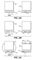
- FIG. 9A shows a first sector being received by a memory system and being stored in the cache memory.
- FIG. 9B shows a second sector being received by a memory system being stored in the cache memory with the first sector.
- FIG. 9C shows a third sector being received by a memory system and being stored in the cache memory, the first two sectors being programmed to the memory array.
- FIG. 10A shows sequential single sectors being received by a memory system having a cache memory.
- FIG. 10B shows a sector being received that replaces a sector of data that is stored in the cache memory.
- FIG. 11 shows a read-modify-write sequence for updating a page of data.
- FIG. 12 shows a memory system that is suitable for implementing an on-chip cache.
- FIG. 13 shows a flowchart for an embodiment of the present invention.
- a flash memory includes a memory cell array and a controller.
- two integrated circuit devices (chips) 11 and 13 include an array 15 of memory cells and various logic circuits 17 .
- the logic circuits 17 interface with a controller 19 on a separate chip through data, command and status circuits, and also provide addressing, data transfer and sensing, and other support to the array 13 .
- a number of memory array chips can be from one to many, depending upon the storage capacity provided.
- the controller and part or the entire array can alternatively be combined onto a single integrated circuit chip but this is currently not an economical alternative.
- a typical controller 19 includes a microprocessor 21 , a program memory 23 primarily to store firmware and a data buffer memory (RAM) 25 primarily for the temporary storage of user data either being written to or read from the memory chips 11 and 13 .
- a program memory may be either volatile or non-volatile.
- Program memory is dedicated to storage of data for controller operation.
- program memory is a Read Only Memory (ROM).
- Circuits 27 interface with the memory array chip(s) and circuits 29 interface with a host though connections 31 . The integrity of data is in this example determined by calculating an ECC with circuits 33 dedicated to calculating the code. As user data is being transferred from the host to the flash memory array for storage, the circuit calculates an ECC from the data and the code is stored in the memory.
- connections 31 of the memory of FIG. 2A mate with connections 31 ′ of a host system, an example of which is given in FIG. 2B .
- Data transfers between the host and the memory of FIG. 2A are through interface circuits 35 .
- a typical host also includes a microprocessor 37 , a ROM 39 for storing firmware code and RAM 41 .
- Other circuits and subsystems 43 often include a high capacity magnetic data storage disk drive, interface circuits for a keyboard, a monitor and the like, depending upon the particular host system.
- hosts include desktop computers, laptop computers, handheld computers, palmtop computers, personal digital assistants (PDAs), MP3 and other audio players, digital cameras, video cameras, electronic game machines, wireless and wired telephony devices, answering machines, voice recorders, network routers and others.
- PDAs personal digital assistants
- MP3 and other audio players
- digital cameras digital cameras
- video cameras electronic game machines
- electronic game machines electronic game machines
- wireless and wired telephony devices answering machines
- voice recorders network routers and others.
- the memory of FIG. 2A may be implemented as a small enclosed card containing the controller and all its memory array circuit devices in a form that is removably connectable with the host of FIG. 2B . That is, mating connections 31 and 31 ′ allow a card to be disconnected and moved to another host, or replaced by connecting another card to the host.
- the memory array devices may be enclosed in a separate card that is electrically and mechanically connectable with a card containing the controller and connections 31 .
- the memory of FIG. 2A may be embedded within the host of FIG. 2B , wherein the connections 31 and 31 ′ are permanently made. In this case, the memory is usually contained within an enclosure of the host along with other components.
- FIG. 3A illustrates a portion of a memory array wherein memory cells are grouped into blocks, the cells in each block being erasable together as part of a single erase operation, usually simultaneously.
- a block is the minimum unit of erase.
- the size of the individual memory cell blocks of FIG. 3A can vary but one commercially practiced form includes a single sector of data in an individual block. The contents of such a data sector are illustrated in FIG. 3B .
- User data 51 are typically 512 bytes.
- overhead data that includes an ECC 53 calculated from the user data, parameters 55 relating to the sector data and/or the block in which the sector is programmed and an ECC 57 calculated from the parameters 55 and any other overhead data that might be included.
- the parameters 55 may include an indication of the bit values assigned to each of the storage states of the memory cells, referred to as their “rotation”. This also has a beneficial effect in wear leveling.
- One or more flags may also be included in the parameters 55 that indicate status or states. Indications of voltage levels to be used for programming and/or erasing the block can also be stored within the parameters 55 , these voltages being updated as the number of cycles experienced by the block and other factors change.
- Other examples of the parameters 55 include an identification of any defective cells within the block, the logical address of the block that is mapped into this physical block and the address of any substitute block in case the primary block is defective.
- the particular combination of parameters 55 that are used in any memory system will vary in accordance with the design. Also, some or all of the overhead data can be stored in blocks dedicated to such a function, rather than in the block containing the user data or to which the overhead data pertains.
- An example block 59 still the minimum unit of erase, contains four pages 0 - 3 , each of which is the minimum unit of programming.
- One or more host sectors of data are stored in each page, usually along with overhead data including at least the ECC calculated from the sector's data and may be in the form of the data sector of FIG. 3B .
- Re-writing the data of an entire block usually involves programming the new data into an erased block of an erase block pool, the original block then being erased and placed in the erase pool.
- the updated data are typically stored in a page of an erased block from the erased block pool and data in the remaining unchanged pages are copied from the original block into the new block.
- the original block is then erased.
- Variations of this large block management technique include writing the updated data into a page of another block without moving data from the original block or erasing it. This results in multiple pages having the same logical address.
- the most recent page of data is identified by some convenient technique such as the time of programming that is recorded as a field in sector or page overhead data.
- FIG. 5 A further multi-sector block arrangement is illustrated in FIG. 5 .
- the total memory cell array is physically divided into two or more planes, four planes 0 - 3 being illustrated.
- Each plane is a sub-array of memory cells that has its own data registers, sense amplifiers, addressing decoders and the like in order to be able to operate largely independently of the other planes. All the planes may be provided on a single integrated circuit device or on multiple devices, an example being to form each plane from one or more distinct integrated circuit devices.
- Each block in the example system of FIG. 5 contains 16 pages P 0 -P 15 , each page having a capacity of one, two or more host data sectors and some overhead data.
- FIG. 6 Yet another memory cell arrangement is illustrated in FIG. 6 .
- Each plane contains a large number of blocks of cells.
- blocks within different planes are logically linked to form metablocks.
- One such metablock is illustrated in FIG. 6 as being formed of block 3 of plane 0 , block 1 of plane 1 , block 1 of plane 2 and block 2 of plane 3 .
- the memory controller assigns and keeps track of the blocks that form the individual metablocks.
- the host system preferably interfaces with the memory system in addressable units of data such as a sector.
- the memory controller may use other units of data that comprise multiple sectors.
- a logical data block is a unit of data comprising data equal to the capacity of an individual metablock.
- Such a logical data block 61 of FIG. 6 is mapped by the controller into the blocks that make up the metablock. All blocks of the metablock are erased together, and pages from each block are preferably programmed and read simultaneously.
- the controller maintains a record of the physical locations where portions of data (for example, sectors) are stored.
- a logical to physical mapping is performed so that the location of a particular sector in the non-volatile memory array may be determined.
- data is written to a new physical location when it is updated so that the logical to physical information is also updated.
- Sectors of data may be maintained in sequential order in a block or may be written in non-sequential order as described in U.S.
- FIG. 7 One block of a memory array of the NAND type is shown in FIG. 7 .
- a large number of column oriented strings of series connected memory cells are connected between a common source 65 of a voltage Vss and one of bit lines BL 0 -BLN that are in turn connected with circuits 67 containing address decoders, drivers, read sense amplifiers and the like.
- one such string contains charge storage transistors 70 , 71 . . . 72 and 74 connected in series between select transistors 77 and 79 at opposite ends of the strings.
- each string contains 16 storage transistors but other numbers are possible.
- Word lines WL 0 -WL 15 extend across one storage transistor of each string and are connected to circuits 81 that contain address decoders and voltage source drivers of the word lines. Voltages on lines 83 and 84 control connection of all the strings in the block together to either the voltage source 65 and/or the bit lines BL 0 -BLN through their select transistors. Data and addresses come from the memory controller.
- Each row of charge storage transistors (memory cells) of the block forms a page that is programmed and read together.
- An appropriate voltage is applied to the word line (WL) of such a page for programming or reading its data while voltages applied to the remaining word lines are selected to render their respective storage transistors conductive.
- WL word line
- previously stored charge levels on unselected rows can be disturbed because of voltages applied across all the strings and to their word lines.
- FIG. 8 shows an example of a memory system 800 utilizing the present invention.
- a memory array 802 has a word line decoder 804 and a bit line decoder 806 connected to memory array 802 along adjacent edges of memory array 802 .
- Word line decoder 804 is connected to the controller 808 .
- Bit line decoder 806 is connected to a cache memory 810 .
- Cache memory 810 is connected to controller 808 .
- cache memory 810 is in-line between controller 808 and bit line decoder 806 .
- Data going between controller 808 and memory array 802 pass through cache memory 810 .
- data sent from controller 808 for storage in memory array 802 pass through cache memory 810 .
- Data may be stored in cache memory 810 before being written to memory array 802 .
- Controller 808 is connected to a host in the example shown in FIG. 8 .
- Memory systems of the type shown may be used in an enclosed card that is removably connected with a host system.
- this memory system may be implemented in a card according to one of the standards discussed above (PCMCIA, CF, MMC, SD).
- the host may be a digital camera, mobile phone or other device that uses memory cards.
- the memory system may be embedded in a host system.
- FIG. 9A shows an addressable unit of data 912 being sent to cache memory 810 that is empty.
- One example of such an addressable unit is a sector of data comprising 512 bytes.
- a sector 912 is received from the host and is stored in the cache memory 810 instead of being written to memory array 802 . This is in contrast to the prior art example of FIG. 1 where, after the sector is transferred to the register, it is written to the memory array.
- sector 912 is stored in a cache memory 810 that may contain four sectors of data. This is because the size of one page (unit of program) for memory array 802 is four sectors. Memory arrays that have larger pages would require larger cache memories.
- a signal may be sent to the host indicating that the sector has been programmed. This enables the host to send more data to the memory system. Because writing to a cache memory is quicker than writing to many non-volatile memory arrays, storing a sector in cache may improve system speed and allow the host to send another sector more rapidly than if a write operation was performed.
- FIG. 9B shows another sector of data 914 being received by the cache memory of FIG. 9B .
- the new sector 914 and the cached sector 912 are compared to determine if they may be written to the memory array in the same page. This determination may be made by comparing the new sector 914 with the physical page location for storing the cached data, here sector 912 .
- the two sectors of data 912 , 914 may be written in the same page. Because they can be written together, the new sector 914 is stored with the cached sector 912 in cache memory 810 .
- a signal is sent to the host indicating that the second sector 914 has been programmed.
- sectors are programmable together if they are logically sequential. Because the controller often sends sectors to the memory array sequentially, such received sectors are often programmable in a single page.
- FIG. 9C shows another sector of data 916 being received by cache memory 810 .
- the new sector 916 is again compared to the cached data.
- the cached data is written to memory array 810 .
- the cache is written to a single page, thus the two sectors 912 , 914 stored in cache memory 810 are written to a single page.
- Writing cache 810 to the memory array 802 empties cache 810 .
- the new sector 916 is then stored in cache 810 .
- the result, shown in FIG. 9C is that two sectors 912 , 914 are stored in a single page without additional copying of pages or any additional erase steps.
- potentially even greater saving of space could be achieved. For example, in a page that comprises four sectors, up to four sectors could be programmed together saving as many as three pages of space in the memory array. For bigger page sizes containing more sectors, the potential saving of space in the memory array is even greater.
- programming the two sectors 912 , 914 required only one write operation where previously two separate write operations would have been used. Because write operations may be time consuming this may increase the speed of data transfer between the host and the memory system. Also, only one page is used to store the two sectors so that space in the memory array is more efficiently used. Once a sector is stored in cache the host may send another sector where previously the host would wait until a write operation was performed.
- FIG. 10A shows programming of sequentially received sectors 101 , 102 , 103 , 104 .
- the sectors may be programmed together in a single page 106 because they are logically sequential or because the memory system allows non-sequential storage of sectors.
- single sectors received from a host are sequential. While four sectors are shown forming a complete page of data in this example, in some cases less than a full page of data may be programmed.
- FIG. 10B shows the situation where the host sends a sector of data 107 that is to replace a sector 108 that was previously sent.
- the new sector 107 and the old sector 108 have the same logical address.
- New sector 107 may replace old sector 108 in cache 810 without ever writing the cached sector 108 to the memory array. This reduces wear on array 802 and also increases the speed of memory system 800 .
- FIG. 11 shows another example of using on-chip cache 810 .
- a page of data 111 is first read from the memory array 802 to the cache memory 810 .
- the data from page 111 is then modified while it is in cache memory 810 .
- the modification is updating one sector of data by replacing the old sector 112 by a new sector 113 .
- multiple pages of data may be updated.
- the data in cache 810 is modified, the data is written back to memory array 802 .
- the data is written back to a page 114 having a different location to the page 111 from which it was read. This is because writing to the same location would require an erase operation, which can only be done for an erase block.
- the controller generally keeps track of where particular data is located in the physical memory by a table or tables that record the logical address to physical address mapping
- the cache memory of this invention is not limited in size to just one page.
- a cache memory may store data for several pages. This allows a received sector to be cached for programming to one of several pages. This increases the chances of combining sectors in the cache memory prior to writing to the memory array and thus increases the memory storage performance.
- the cache memory may be implemented using the data registers that are employed in certain memory systems. This provides a relatively small, simple cache memory that is on the same chip as the memory array. Thus, the present invention may be implemented without requiring additional hardware.
- registers are comprised of volatile latches.
- the register or registers connected to a memory array or sub-array typically store data that is equal to the data stored in one row of the memory array or sub-array. In other examples, data for two or more rows of the array are stored in registers. This makes such registers suitable for caching data that is to be programmed to a wide page that extends along a row of the memory array.
- FIG. 12 shows an example of a memory array 400 having a master register 403 and a slave register 404 that may be used as a cache memory.
- a write operation from the cache memory to the memory array may be triggered by different events.
- One example, described above, is receiving a sector of data that is not programmable with the cached data.
- Another example is receiving a signal from the host indicating that a write operation is required.
- Another triggering event is the detection of a low power condition.
- a low power condition could be detected by a circuit in the memory system. For example, detection of an undervoltage condition (low voltage detection, or LVD) may be used to indicate a low power condition is imminent. Alternatively, the low power condition could be detected by the host and a signal could be sent to the memory system indicating the condition.
- Low power conditions are a particular problem where memory systems are implemented in removable cards connected to a host.
- One way to save cached data during a low power condition is to write it to the memory array.
- the cached data is multi-level data, it may be saved as binary data.
- binary data is quicker to write than multi-level data and requires less power. Examples of writing both multi-level data and binary data in the same memory array are provided in U.S. Pat. No. 6,717,847, entitled, “Selective operation of a multi-state non-volatile memory system in a binary mode,” which patent is hereby incorporated by reference in its entirety.
- Cached data may be written to a predetermined address in the memory array. When low power is detected, the state machine begins programming the data in cache to the predetermined address in the memory array. No program command is needed.
- This function may be enabled and disabled by the controller.
- the controller checks to see if there is data written at the predetermined address. If there is data there, this indicates to the controller that the data was in cache memory during the last power-down. Thus, the controller can load the data to the cache memory. The data is then erased from the memory array so that the predetermined address is available for subsequent use. If a power-down occurs without data in the cache, no data is written to the predetermined address and upon the subsequent power-up the controller simply verifies that there is no data there and hence no data to restore to the cache memory.
- Temporary power may be provided by a power storage device within the memory system such as a capacitor.
- a signal may be issued by the host that a low power condition is imminent. For example, where the card is secured in the host system, opening a door to access the card may cause the host to signal that a write to the memory array is required. The volatile cache is then written to the memory array before the card is removed from the host.
- the cached data may also be written to the memory array after a period of inactivity.
- the cache maintains data that is to be stored in the array.
- all data remaining in the cache memory is written to the memory array. This prepares the memory system for power loss.
- FIG. 13 shows a flowchart for a new command or LVD being received by a controller in a memory system. If the command is a write command 330 then a host sector write sequence 332 is begun for a sector. If the cache is not valid 334 (i.e. if there is no data in the cache) then the sector is transferred to cache 338 . If the cache is valid 334 (i.e. there is data in the cache) then the sector is compared to the data in cache to determine whether the sector has a physical address in the cache range 336 . For a single-page cache, this means that the sector has been assigned by the controller to the same page in the memory array that the cached data has been assigned to.
- this also means that the cached data and the sector have logical addresses within the same range. However, in some systems, sectors may be stored together even where there is a logical address gap between them. If the sector is in the cache range then it is stored with the previously cached data in the cache memory 338 . If the sector is not in the cache range, a cache flush process is carried out 340 . This means that the contents of the cache are programmed to the memory array. When the program operation has been completed 342 , the sector is transferred to cache memory. If there is more data to be written 344 , then this cycle is repeated for subsequent sectors. If there is no more data to be written, then the system may wait for a predetermined period 346 before flushing the cache 348 .
- the system waits for a new command 352 .
- a command is received that is not a write command 330
- the cache is flushed 354 and, when the flush is complete 356 , it is determined if an LVD has occurred 358 . If an LVD has occurred, then the system may enter a sleep mode 360 because the contents of the cache are already saved in non-volatile memory. If an LVD has not occurred, then the new command is processed according to a predefined process for that command 362 .
Landscapes
- Engineering & Computer Science (AREA)
- Theoretical Computer Science (AREA)
- Physics & Mathematics (AREA)
- General Engineering & Computer Science (AREA)
- General Physics & Mathematics (AREA)
- Microelectronics & Electronic Packaging (AREA)
- Read Only Memory (AREA)
- Memory System Of A Hierarchy Structure (AREA)
- Techniques For Improving Reliability Of Storages (AREA)
Abstract
Description
Claims (26)
Priority Applications (9)
| Application Number | Priority Date | Filing Date | Title |
|---|---|---|---|
| US11/021,200 US7882299B2 (en) | 2004-12-21 | 2004-12-21 | System and method for use of on-chip non-volatile memory write cache |
| AT05854199T ATE469420T1 (en) | 2004-12-21 | 2005-12-14 | SYSTEM AND METHOD FOR USING AN ON-CHIP WRITE CACHE OF NON-VOLATILE MEMORY |
| DE602005021544T DE602005021544D1 (en) | 2004-12-21 | 2005-12-14 | SYSTEM AND METHOD FOR USING AN ON-CHIP SCROLL OF A NON-VOLATILE MEMORY |
| KR1020077014037A KR101040961B1 (en) | 2004-12-21 | 2005-12-14 | System and method for using on-chip nonvolatile memory write cache |
| EP05854199A EP1829047B1 (en) | 2004-12-21 | 2005-12-14 | System and method for use of on-chip non-volatile memory write cache |
| KR1020097024956A KR20100022026A (en) | 2004-12-21 | 2005-12-14 | System and method for use of on-chip non-volatile memory write cache |
| JP2007548312A JP4834676B2 (en) | 2004-12-21 | 2005-12-14 | System and method using on-chip non-volatile memory write cache |
| PCT/US2005/045431 WO2006068916A1 (en) | 2004-12-21 | 2005-12-14 | System and method for use of on-chip non-volatile memory write cache |
| TW094145663A TW200634823A (en) | 2004-12-21 | 2005-12-21 | System and method for use of on-chip non-volatile memory write cache |
Applications Claiming Priority (1)
| Application Number | Priority Date | Filing Date | Title |
|---|---|---|---|
| US11/021,200 US7882299B2 (en) | 2004-12-21 | 2004-12-21 | System and method for use of on-chip non-volatile memory write cache |
Publications (2)
| Publication Number | Publication Date |
|---|---|
| US20060136656A1 US20060136656A1 (en) | 2006-06-22 |
| US7882299B2 true US7882299B2 (en) | 2011-02-01 |
Family
ID=36283836
Family Applications (1)
| Application Number | Title | Priority Date | Filing Date |
|---|---|---|---|
| US11/021,200 Active 2027-05-01 US7882299B2 (en) | 2004-12-21 | 2004-12-21 | System and method for use of on-chip non-volatile memory write cache |
Country Status (8)
| Country | Link |
|---|---|
| US (1) | US7882299B2 (en) |
| EP (1) | EP1829047B1 (en) |
| JP (1) | JP4834676B2 (en) |
| KR (2) | KR20100022026A (en) |
| AT (1) | ATE469420T1 (en) |
| DE (1) | DE602005021544D1 (en) |
| TW (1) | TW200634823A (en) |
| WO (1) | WO2006068916A1 (en) |
Cited By (11)
| Publication number | Priority date | Publication date | Assignee | Title |
|---|---|---|---|---|
| US20120054421A1 (en) * | 2010-08-25 | 2012-03-01 | Hitachi, Ltd. | Information device equipped with cache memories, apparatus and program using the same device |
| US20140254263A1 (en) * | 2013-03-07 | 2014-09-11 | Sandisk Technologies Inc. | Write Sequence Providing Write Abort Protection |
| US8914592B2 (en) | 2010-12-01 | 2014-12-16 | Kabushiki Kaisha Toshiba | Data storage apparatus with nonvolatile memories and method for controlling nonvolatile memories |
| US9218282B2 (en) | 2013-10-31 | 2015-12-22 | Micron Technology, Inc. | Memory system data management |
| TWI549134B (en) * | 2014-10-30 | 2016-09-11 | 華邦電子股份有限公司 | Nand type flash memory and programming method thereof |
| US9891694B2 (en) | 2012-12-22 | 2018-02-13 | Qualcomm Incorporated | Reducing power consumption of volatile memory via use of non-volatile memory |
| TWI619017B (en) * | 2017-01-23 | 2018-03-21 | 美光科技公司 | Partially written block treatment |
| US10811071B1 (en) | 2019-05-17 | 2020-10-20 | Yangtze Memory Technologies Co., Ltd. | Three-dimensional memory device with static random-access memory |
| TWI713200B (en) * | 2019-05-17 | 2020-12-11 | 大陸商長江存儲科技有限責任公司 | Operation of caching process of a 3d memory device having static random accessory memory |
| US11249920B2 (en) | 2018-12-31 | 2022-02-15 | Knu-Industry Cooperation Foundation | Non-volatile memory device using efficient page collection mapping in association with cache and method of operating the same |
| US11816343B2 (en) | 2020-11-30 | 2023-11-14 | Western Digital Technologies, Inc. | Data storage device enabling latches of non-volatile memory dies for use as externally-accessible volatile memory |
Families Citing this family (76)
| Publication number | Priority date | Publication date | Assignee | Title |
|---|---|---|---|---|
| US7356641B2 (en) * | 2001-08-28 | 2008-04-08 | International Business Machines Corporation | Data management in flash memory |
| US9010645B2 (en) * | 2003-06-13 | 2015-04-21 | Michael Arnouse | Portable computing system and portable computer for use with same |
| US7702848B2 (en) * | 2004-06-10 | 2010-04-20 | Marvell World Trade Ltd. | Adaptive storage system including hard disk drive with flash interface |
| US7788427B1 (en) * | 2005-05-05 | 2010-08-31 | Marvell International Ltd. | Flash memory interface for disk drive |
| US7617359B2 (en) * | 2004-06-10 | 2009-11-10 | Marvell World Trade Ltd. | Adaptive storage system including hard disk drive with flash interface |
| US7730335B2 (en) | 2004-06-10 | 2010-06-01 | Marvell World Trade Ltd. | Low power computer with main and auxiliary processors |
| US7882299B2 (en) | 2004-12-21 | 2011-02-01 | Sandisk Corporation | System and method for use of on-chip non-volatile memory write cache |
| KR101185614B1 (en) * | 2005-01-31 | 2012-09-28 | 삼성전자주식회사 | Power Saving Method and Apparatus for Mobile System with Blocking the Power of the Module |
| EP2016494A4 (en) * | 2006-02-14 | 2010-02-03 | Atmel Corp | Writing to and configuring flash memory |
| US8245109B2 (en) * | 2006-03-31 | 2012-08-14 | Hewlett-Packard Development Company, L.P. | Error checking and correction (ECC) system and method |
| US20090282185A1 (en) * | 2006-06-30 | 2009-11-12 | Nxp B.V. | Flash memory device and a method for using the same |
| US20080263324A1 (en) | 2006-08-10 | 2008-10-23 | Sehat Sutardja | Dynamic core switching |
| JP4304676B2 (en) * | 2006-10-31 | 2009-07-29 | 日本電気株式会社 | Data transfer apparatus, data transfer method, and computer apparatus |
| KR100833512B1 (en) * | 2006-12-08 | 2008-05-29 | 한국전자통신연구원 | Sensing data storage device and its method of tag |
| US7502255B2 (en) * | 2007-03-07 | 2009-03-10 | Sandisk Corporation | Method for cache page copy in a non-volatile memory |
| US7499320B2 (en) | 2007-03-07 | 2009-03-03 | Sandisk Corporation | Non-volatile memory with cache page copy |
| US8140908B2 (en) * | 2007-06-22 | 2012-03-20 | Microsoft Corporation | System and method of client side analysis for identifying failing RAM after a user mode or kernel mode exception |
| JP4743174B2 (en) * | 2007-06-29 | 2011-08-10 | Tdk株式会社 | MEMORY CONTROLLER, FLASH MEMORY SYSTEM HAVING MEMORY CONTROLLER, AND FLASH MEMORY CONTROL METHOD |
| US9032154B2 (en) * | 2007-12-13 | 2015-05-12 | Sandisk Technologies Inc. | Integration of secure data transfer applications for generic IO devices |
| US20090201748A1 (en) * | 2008-02-11 | 2009-08-13 | Sony Corporation | Removable nonvolatile memory system with destructive read |
| USRE49124E1 (en) | 2008-02-13 | 2022-07-05 | Arnouse Digital Devices Corp. | Mobile data center |
| US11113228B2 (en) | 2008-02-13 | 2021-09-07 | Arnouse Digital Devices Corporation | Portable computing system and portable computer for use with same |
| US10235323B2 (en) | 2008-02-13 | 2019-03-19 | Michael Arnouse | Portable computing system and portable computer for use with same |
| TWI350453B (en) * | 2008-06-13 | 2011-10-11 | Phison Electronics Corp | Method, system and controller thereof for transmitting and dispatching data stream |
| TWI399651B (en) * | 2008-09-12 | 2013-06-21 | Communication protocol method and system for input / output device | |
| TWI405209B (en) * | 2009-04-01 | 2013-08-11 | Phison Electronics Corp | Data management method and flash memory stroage system and controller using the same |
| US8832353B2 (en) * | 2009-04-07 | 2014-09-09 | Sandisk Technologies Inc. | Host stop-transmission handling |
| US8027195B2 (en) * | 2009-06-05 | 2011-09-27 | SanDisk Technologies, Inc. | Folding data stored in binary format into multi-state format within non-volatile memory devices |
| US8102705B2 (en) | 2009-06-05 | 2012-01-24 | Sandisk Technologies Inc. | Structure and method for shuffling data within non-volatile memory devices |
| US8132045B2 (en) * | 2009-06-16 | 2012-03-06 | SanDisk Technologies, Inc. | Program failure handling in nonvolatile memory |
| US8307241B2 (en) * | 2009-06-16 | 2012-11-06 | Sandisk Technologies Inc. | Data recovery in multi-level cell nonvolatile memory |
| US20110002169A1 (en) * | 2009-07-06 | 2011-01-06 | Yan Li | Bad Column Management with Bit Information in Non-Volatile Memory Systems |
| EP2317442A1 (en) | 2009-10-29 | 2011-05-04 | Thomson Licensing | Solid state memory with reduced number of partially filled pages |
| US20110153912A1 (en) * | 2009-12-18 | 2011-06-23 | Sergey Anatolievich Gorobets | Maintaining Updates of Multi-Level Non-Volatile Memory in Binary Non-Volatile Memory |
| US8144512B2 (en) * | 2009-12-18 | 2012-03-27 | Sandisk Technologies Inc. | Data transfer flows for on-chip folding |
| US8468294B2 (en) * | 2009-12-18 | 2013-06-18 | Sandisk Technologies Inc. | Non-volatile memory with multi-gear control using on-chip folding of data |
| US8725935B2 (en) | 2009-12-18 | 2014-05-13 | Sandisk Technologies Inc. | Balanced performance for on-chip folding of non-volatile memories |
| TWI424438B (en) * | 2009-12-30 | 2014-01-21 | Asolid Technology Co Ltd | Nonvolatile memory control apparatus and multi-stage resorting method thereof |
| WO2011082703A1 (en) * | 2010-01-08 | 2011-07-14 | Hyperstone Gmbh | Method for managing flash memories with multi-level cells |
| KR20120091648A (en) * | 2011-02-09 | 2012-08-20 | 삼성전자주식회사 | Non-volatile memory, system having the same, and method of programming the same |
| US20120221809A1 (en) * | 2011-02-28 | 2012-08-30 | Hitachi, Ltd. | Storage apparatus and data processing method of the same |
| US9342446B2 (en) | 2011-03-29 | 2016-05-17 | SanDisk Technologies, Inc. | Non-volatile memory system allowing reverse eviction of data updates to non-volatile binary cache |
| US9898402B2 (en) | 2011-07-01 | 2018-02-20 | Micron Technology, Inc. | Unaligned data coalescing |
| US8687453B2 (en) * | 2011-10-12 | 2014-04-01 | Wisconsin Alumni Research Foundation | Energy efficient processor having heterogeneous cache |
| US9911470B2 (en) | 2011-12-15 | 2018-03-06 | Nvidia Corporation | Fast-bypass memory circuit |
| US8842473B2 (en) | 2012-03-15 | 2014-09-23 | Sandisk Technologies Inc. | Techniques for accessing column selecting shift register with skipped entries in non-volatile memories |
| US10101769B2 (en) | 2012-04-10 | 2018-10-16 | Michael Arnouse | Mobile data center |
| US8681548B2 (en) | 2012-05-03 | 2014-03-25 | Sandisk Technologies Inc. | Column redundancy circuitry for non-volatile memory |
| CN103632712A (en) | 2012-08-27 | 2014-03-12 | 辉达公司 | Memory cell and memory |
| US9058126B2 (en) * | 2012-09-10 | 2015-06-16 | Texas Instruments Incorporated | Nonvolatile logic array with retention flip flops to reduce switching power during wakeup |
| US9076506B2 (en) | 2012-09-28 | 2015-07-07 | Sandisk Technologies Inc. | Variable rate parallel to serial shift register |
| US8897080B2 (en) | 2012-09-28 | 2014-11-25 | Sandisk Technologies Inc. | Variable rate serial to parallel shift register |
| US9490035B2 (en) | 2012-09-28 | 2016-11-08 | SanDisk Technologies, Inc. | Centralized variable rate serializer and deserializer for bad column management |
| US9685207B2 (en) | 2012-12-04 | 2017-06-20 | Nvidia Corporation | Sequential access memory with master-slave latch pairs and method of operating |
| US9081712B2 (en) * | 2012-12-21 | 2015-07-14 | Dell Products, L.P. | System and method for using solid state storage systems as a cache for the storage of temporary data |
| US9405621B2 (en) * | 2012-12-28 | 2016-08-02 | Super Talent Technology, Corp. | Green eMMC device (GeD) controller with DRAM data persistence, data-type splitting, meta-page grouping, and diversion of temp files for enhanced flash endurance |
| US9281817B2 (en) | 2012-12-31 | 2016-03-08 | Nvidia Corporation | Power conservation using gray-coded address sequencing |
| US9037902B2 (en) | 2013-03-15 | 2015-05-19 | Sandisk Technologies Inc. | Flash memory techniques for recovering from write interrupt resulting from voltage fault |
| US10141930B2 (en) | 2013-06-04 | 2018-11-27 | Nvidia Corporation | Three state latch |
| US20150089118A1 (en) * | 2013-09-20 | 2015-03-26 | Sandisk Technologies Inc. | Methods, systems, and computer readable media for partition and cache restore |
| US9323614B2 (en) | 2013-11-06 | 2016-04-26 | Wisconsin Alumni Research Foundation | Dynamic error handling for on-chip memory structures |
| KR20160007972A (en) * | 2014-07-10 | 2016-01-21 | 삼성전자주식회사 | Nonvolatile memory device, memory controller, and operating method of the same |
| US9934872B2 (en) | 2014-10-30 | 2018-04-03 | Sandisk Technologies Llc | Erase stress and delta erase loop count methods for various fail modes in non-volatile memory |
| US9224502B1 (en) | 2015-01-14 | 2015-12-29 | Sandisk Technologies Inc. | Techniques for detection and treating memory hole to local interconnect marginality defects |
| US10032524B2 (en) | 2015-02-09 | 2018-07-24 | Sandisk Technologies Llc | Techniques for determining local interconnect defects |
| US9269446B1 (en) | 2015-04-08 | 2016-02-23 | Sandisk Technologies Inc. | Methods to improve programming of slow cells |
| US9564219B2 (en) | 2015-04-08 | 2017-02-07 | Sandisk Technologies Llc | Current based detection and recording of memory hole-interconnect spacing defects |
| KR102739276B1 (en) * | 2016-09-20 | 2024-12-05 | 삼성전자주식회사 | Method of operating memory controller and methods of operating devices having the same |
| US10318423B2 (en) | 2016-12-14 | 2019-06-11 | Macronix International Co., Ltd. | Methods and systems for managing physical information of memory units in a memory device |
| US10318417B2 (en) * | 2017-03-31 | 2019-06-11 | Intel Corporation | Persistent caching of memory-side cache content |
| FR3072476A1 (en) * | 2017-10-13 | 2019-04-19 | Proton World International N.V. | MEMORY LOGIC UNIT FOR FLASH MEMORY |
| US11037627B2 (en) | 2017-11-29 | 2021-06-15 | Western Digital Technologies, Inc. | Cell block allocation for hybrid dual write |
| KR102456176B1 (en) * | 2020-05-21 | 2022-10-19 | 에스케이하이닉스 주식회사 | Memory controller and operating method thereof |
| US11573891B2 (en) | 2019-11-25 | 2023-02-07 | SK Hynix Inc. | Memory controller for scheduling commands based on response for receiving write command, storage device including the memory controller, and operating method of the memory controller and the storage device |
| US11966621B2 (en) * | 2022-02-17 | 2024-04-23 | Sandisk Technologies Llc | Non-volatile storage system with program execution decoupled from dataload |
| US12197329B2 (en) * | 2022-12-09 | 2025-01-14 | Advanced Micro Devices, Inc. | Range-based cache flushing |
Citations (87)
| Publication number | Priority date | Publication date | Assignee | Title |
|---|---|---|---|---|
| US4725945A (en) | 1984-09-18 | 1988-02-16 | International Business Machines Corp. | Distributed cache in dynamic rams |
| US5043940A (en) | 1988-06-08 | 1991-08-27 | Eliyahou Harari | Flash EEPROM memory systems having multistate storage cells |
| US5070032A (en) | 1989-03-15 | 1991-12-03 | Sundisk Corporation | Method of making dense flash eeprom semiconductor memory structures |
| US5095344A (en) | 1988-06-08 | 1992-03-10 | Eliyahou Harari | Highly compact eprom and flash eeprom devices |
| US5172338A (en) | 1989-04-13 | 1992-12-15 | Sundisk Corporation | Multi-state EEprom read and write circuits and techniques |
| EP0557968A2 (en) | 1992-02-25 | 1993-09-01 | Fuji Photo Film Co., Ltd. | Method of rewriting data in EEPROM, and EEPROM card |
| EP0566306A2 (en) | 1992-04-16 | 1993-10-20 | Hitachi, Ltd. | Semiconductor memory device |
| US5276829A (en) * | 1988-05-31 | 1994-01-04 | Kabushiki Kaisha Toshiba | Data processing system including cache memory for rapidly converting a logical address into a physical address using shared memory flag |
| US5313421A (en) | 1992-01-14 | 1994-05-17 | Sundisk Corporation | EEPROM with split gate source side injection |
| US5315541A (en) | 1992-07-24 | 1994-05-24 | Sundisk Corporation | Segmented column memory array |
| US5343063A (en) | 1990-12-18 | 1994-08-30 | Sundisk Corporation | Dense vertical programmable read only memory cell structure and processes for making them |
| US5418752A (en) | 1989-04-13 | 1995-05-23 | Sundisk Corporation | Flash EEPROM system with erase sector select |
| US5438549A (en) * | 1994-02-28 | 1995-08-01 | Intel Corporation | Nonvolatile memory with volatile memory buffer and a backup power supply system |
| US5530673A (en) * | 1993-04-08 | 1996-06-25 | Hitachi, Ltd. | Flash memory control method and information processing system therewith |
| US5532962A (en) | 1992-05-20 | 1996-07-02 | Sandisk Corporation | Soft errors handling in EEPROM devices |
| US5570315A (en) | 1993-09-21 | 1996-10-29 | Kabushiki Kaisha Toshiba | Multi-state EEPROM having write-verify control circuit |
| US5586291A (en) * | 1994-12-23 | 1996-12-17 | Emc Corporation | Disk controller with volatile and non-volatile cache memories |
| US5606532A (en) | 1995-03-17 | 1997-02-25 | Atmel Corporation | EEPROM array with flash-like core |
| US5661053A (en) | 1994-05-25 | 1997-08-26 | Sandisk Corporation | Method of making dense flash EEPROM cell array and peripheral supporting circuits formed in deposited field oxide with the use of spacers |
| US5677872A (en) | 1995-05-31 | 1997-10-14 | Sandisk Corporation | Low voltage erase of a flash EEPROM system having a common erase electrode for two individual erasable sectors |
| US5712179A (en) | 1995-10-31 | 1998-01-27 | Sandisk Corporation | Method of making triple polysilicon flash EEPROM arrays having a separate erase gate for each row of floating gates |
| US5726937A (en) * | 1994-01-31 | 1998-03-10 | Norand Corporation | Flash memory system having memory cache |
| US5774397A (en) | 1993-06-29 | 1998-06-30 | Kabushiki Kaisha Toshiba | Non-volatile semiconductor memory device and method of programming a non-volatile memory cell to a predetermined state |
| US5798968A (en) | 1996-09-24 | 1998-08-25 | Sandisk Corporation | Plane decode/virtual sector architecture |
| US5802554A (en) * | 1995-02-28 | 1998-09-01 | Panasonic Technologies Inc. | Method and system for reducing memory access latency by providing fine grain direct access to flash memory concurrent with a block transfer therefrom |
| US5890192A (en) | 1996-11-05 | 1999-03-30 | Sandisk Corporation | Concurrent write of multiple chunks of data into multiple subarrays of flash EEPROM |
| US5909449A (en) | 1997-09-08 | 1999-06-01 | Invox Technology | Multibit-per-cell non-volatile memory with error detection and correction |
| US5930167A (en) | 1997-07-30 | 1999-07-27 | Sandisk Corporation | Multi-state non-volatile flash memory capable of being its own two state write cache |
| US5937423A (en) | 1996-12-26 | 1999-08-10 | Intel Corporation | Register interface for flash EEPROM memory arrays |
| US5956744A (en) * | 1995-09-08 | 1999-09-21 | Texas Instruments Incorporated | Memory configuration cache with multilevel hierarchy least recently used cache entry replacement |
| US5996047A (en) * | 1996-07-01 | 1999-11-30 | Sun Microsystems, Inc. | Method and apparatus for caching file control information corresponding to a second file block in a first file block |
| US6000006A (en) * | 1997-08-25 | 1999-12-07 | Bit Microsystems, Inc. | Unified re-map and cache-index table with dual write-counters for wear-leveling of non-volatile flash RAM mass storage |
| US6026027A (en) * | 1994-01-31 | 2000-02-15 | Norand Corporation | Flash memory system having memory cache |
| US6035347A (en) * | 1997-12-19 | 2000-03-07 | International Business Machines Corporation | Secure store implementation on common platform storage subsystem (CPSS) by storing write data in non-volatile buffer |
| US6046935A (en) | 1996-03-18 | 2000-04-04 | Kabushiki Kaisha Toshiba | Semiconductor device and memory system |
| US6078520A (en) * | 1993-04-08 | 2000-06-20 | Hitachi, Ltd. | Flash memory control method and information processing system therewith |
| US6222762B1 (en) | 1992-01-14 | 2001-04-24 | Sandisk Corporation | Multi-state memory |
| US6249841B1 (en) | 1998-12-03 | 2001-06-19 | Ramtron International Corporation | Integrated circuit memory device and method incorporating flash and ferroelectric random access memory arrays |
| US6263398B1 (en) | 1998-02-10 | 2001-07-17 | Ramtron International Corporation | Integrated circuit memory device incorporating a non-volatile memory array and a relatively faster access time memory cache |
| US6272587B1 (en) * | 1996-09-30 | 2001-08-07 | Cummins Engine Company, Inc. | Method and apparatus for transfer of data between cache and flash memory in an internal combustion engine control system |
| US20010012222A1 (en) * | 1999-12-20 | 2001-08-09 | Yukio Terasaki | Memory controller for flash memory system and method for accessing flash memory device |
| US20010034809A1 (en) * | 1995-09-28 | 2001-10-25 | Takeshi Ogawa | Selecting erase method based on type of power supply for flash eeprom |
| US6329687B1 (en) * | 2000-01-27 | 2001-12-11 | Advanced Micro Devices, Inc. | Two bit flash cell with two floating gate regions |
| US20010052060A1 (en) | 1999-07-12 | 2001-12-13 | Liewei Bao | Buffering system bus for external-memory access |
| WO2002005285A2 (en) | 2000-07-07 | 2002-01-17 | Lexar Media, Inc. | Flash memory architecture implementing simultaneously programmable multiple flash memory banks that are host compatible |
| US20020013874A1 (en) | 2000-06-27 | 2002-01-31 | Hans-Joachim Gelke | Integrated circuit with flash |
| US6349056B1 (en) | 2000-12-28 | 2002-02-19 | Sandisk Corporation | Method and structure for efficient data verification operation for non-volatile memories |
| US6405323B1 (en) * | 1999-03-30 | 2002-06-11 | Silicon Storage Technology, Inc. | Defect management for interface to electrically-erasable programmable read-only memory |
| US6412045B1 (en) * | 1995-05-23 | 2002-06-25 | Lsi Logic Corporation | Method for transferring data from a host computer to a storage media using selectable caching strategies |
| US20020097594A1 (en) * | 2000-11-30 | 2002-07-25 | Bruce Ricardo H. | Parallel erase operations in memory systems |
| US6426893B1 (en) | 2000-02-17 | 2002-07-30 | Sandisk Corporation | Flash eeprom system with simultaneous multiple data sector programming and storage of physical block characteristics in other designated blocks |
| US6434669B1 (en) | 1999-09-07 | 2002-08-13 | International Business Machines Corporation | Method of cache management to dynamically update information-type dependent cache policies |
| US6456528B1 (en) * | 2001-09-17 | 2002-09-24 | Sandisk Corporation | Selective operation of a multi-state non-volatile memory system in a binary mode |
| US20020144059A1 (en) * | 2001-03-28 | 2002-10-03 | Kendall Terry L. | Flash memory low-latency cache |
| US6470422B2 (en) | 1998-12-08 | 2002-10-22 | Intel Corporation | Buffer memory management in a system having multiple execution entities |
| US6483748B2 (en) | 2000-06-05 | 2002-11-19 | Mitsubishi Denki Kabushiki Kaisha | Nonvolatile memory with background operation function |
| US20020174291A1 (en) | 2001-05-15 | 2002-11-21 | International Business Machines Corporation | High speed embedded dram with sram-like interface |
| US20020185337A1 (en) | 2001-06-11 | 2002-12-12 | Hitachi, Ltd. | Semiconductor device with non-volatile memory and random access memory |
| US6510495B1 (en) | 1999-11-19 | 2003-01-21 | Nec Corporation | Data write method into nonvolatile memory, information processing device and recording medium |
| US6522580B2 (en) | 2001-06-27 | 2003-02-18 | Sandisk Corporation | Operating techniques for reducing effects of coupling between storage elements of a non-volatile memory operated in multiple data states |
| US6549977B1 (en) * | 2001-05-23 | 2003-04-15 | 3Ware, Inc. | Use of deferred write completion interrupts to increase the performance of disk operations |
| US20030109093A1 (en) | 2001-10-31 | 2003-06-12 | Eliyahou Harari | Multi-state non-volatile integrated circuit memory systems that employ dielectric storage elements |
| US6601137B1 (en) * | 2000-04-19 | 2003-07-29 | Western Digital Technologies, Inc. | Range-based cache control system and method |
| US6611938B1 (en) * | 1999-06-28 | 2003-08-26 | Kabushiki Kaisha Toshiba | Flash memory |
| US20030163629A1 (en) * | 2002-02-22 | 2003-08-28 | Conley Kevin M. | Pipelined parallel programming operation in a non-volatile memory system |
| US20030201904A1 (en) * | 2002-04-24 | 2003-10-30 | Schlumbergersema Inc., | Method of using flash memory for storing metering data |
| US6647499B1 (en) | 2000-01-26 | 2003-11-11 | International Business Machines Corporation | System for powering down a disk storage device to an idle state upon trnsfer to an intermediate storage location accessible by system processor |
| US20030233513A1 (en) * | 2002-06-12 | 2003-12-18 | Nec Corporation | Information processing system and cache flash control method used for the same |
| US6717847B2 (en) | 2001-09-17 | 2004-04-06 | Sandisk Corporation | Selective operation of a multi-state non-volatile memory system in a binary mode |
| US6725321B1 (en) * | 1999-02-17 | 2004-04-20 | Lexar Media, Inc. | Memory system |
| US6763424B2 (en) | 2001-01-19 | 2004-07-13 | Sandisk Corporation | Partial block data programming and reading operations in a non-volatile memory |
| US20040193782A1 (en) * | 2003-03-26 | 2004-09-30 | David Bordui | Nonvolatile intelligent flash cache memory |
| US20040213045A1 (en) * | 2003-04-25 | 2004-10-28 | Kabushiki Kaisha Toshiba | Semiconductor integrated circuit device |
| US6822899B1 (en) * | 2002-12-23 | 2004-11-23 | Cypress Semiconductor Corporation | Method of protecting flash memory from data corruption during fast power down events |
| US20050050261A1 (en) * | 2003-08-27 | 2005-03-03 | Thomas Roehr | High density flash memory with high speed cache data interface |
| US20050066121A1 (en) * | 2003-09-24 | 2005-03-24 | Keeler Stanton M. | Multi-level caching in data storage devices |
| US20050080994A1 (en) * | 2003-10-14 | 2005-04-14 | International Business Machines Corporation | Method of dynamically controlling cache size |
| US20050125601A1 (en) * | 2003-12-04 | 2005-06-09 | Ehrlich Richard M. | HDD with rapid availability of critical data after critical event |
| US20050144360A1 (en) * | 2003-12-30 | 2005-06-30 | Bennett Alan D. | Non-volatile memory and method with block management system |
| US6941412B2 (en) | 2002-08-29 | 2005-09-06 | Sandisk Corporation | Symbol frequency leveling in a storage system |
| US20050251617A1 (en) * | 2004-05-07 | 2005-11-10 | Sinclair Alan W | Hybrid non-volatile memory system |
| US20050257120A1 (en) | 2004-05-13 | 2005-11-17 | Gorobets Sergey A | Pipelined data relocation and improved chip architectures |
| US20050268025A1 (en) | 2004-05-27 | 2005-12-01 | Peter Smith | Configurable ready/busy control |
| WO2006068916A1 (en) | 2004-12-21 | 2006-06-29 | Sandisk Corporation | System and method for use of on-chip non-volatile memory write cache |
| US20060161722A1 (en) * | 2004-12-16 | 2006-07-20 | Bennett Alan D | Scratch pad block |
| US7113432B2 (en) * | 2000-09-14 | 2006-09-26 | Sandisk Corporation | Compressed event counting technique and application to a flash memory system |
| US7480760B2 (en) * | 2003-12-17 | 2009-01-20 | Wegener Communications, Inc. | Rotational use of memory to minimize write cycles |
Family Cites Families (9)
| Publication number | Priority date | Publication date | Assignee | Title |
|---|---|---|---|---|
| US5087975A (en) * | 1990-11-09 | 1992-02-11 | Zenith Electronics Corporation | VSB HDTV transmission system with reduced NTSC co-channel interference |
| JP2549034B2 (en) * | 1991-07-22 | 1996-10-30 | 株式会社メルコ | Storage device |
| JPH05216775A (en) * | 1991-10-29 | 1993-08-27 | Hitachi Ltd | Semiconductor memory device |
| JPH07146820A (en) * | 1993-04-08 | 1995-06-06 | Hitachi Ltd | Flash memory control method and information processing apparatus using the same |
| JP2000132983A (en) * | 1998-10-26 | 2000-05-12 | Sony Corp | Information recording medium element, information recording device and information recording method, and information reproducing device and information reproducing method |
| JP2000276402A (en) * | 1999-03-24 | 2000-10-06 | Kokusai Electric Co Ltd | Flash memory driving method and flash memory device |
| JP2002222120A (en) * | 2001-01-26 | 2002-08-09 | Sony Corp | Memory access management device and management method |
| JP4563715B2 (en) * | 2003-04-29 | 2010-10-13 | 三星電子株式会社 | Flash memory device having partial copyback operation mode |
| US20060268916A1 (en) * | 2005-05-09 | 2006-11-30 | Sarkar Susanta P | Reliable short messaging service |
-
2004
- 2004-12-21 US US11/021,200 patent/US7882299B2/en active Active
-
2005
- 2005-12-14 EP EP05854199A patent/EP1829047B1/en not_active Expired - Lifetime
- 2005-12-14 JP JP2007548312A patent/JP4834676B2/en not_active Expired - Lifetime
- 2005-12-14 DE DE602005021544T patent/DE602005021544D1/en not_active Expired - Lifetime
- 2005-12-14 AT AT05854199T patent/ATE469420T1/en not_active IP Right Cessation
- 2005-12-14 WO PCT/US2005/045431 patent/WO2006068916A1/en not_active Ceased
- 2005-12-14 KR KR1020097024956A patent/KR20100022026A/en not_active Withdrawn
- 2005-12-14 KR KR1020077014037A patent/KR101040961B1/en not_active Expired - Fee Related
- 2005-12-21 TW TW094145663A patent/TW200634823A/en unknown
Patent Citations (104)
| Publication number | Priority date | Publication date | Assignee | Title |
|---|---|---|---|---|
| US4725945A (en) | 1984-09-18 | 1988-02-16 | International Business Machines Corp. | Distributed cache in dynamic rams |
| US5276829A (en) * | 1988-05-31 | 1994-01-04 | Kabushiki Kaisha Toshiba | Data processing system including cache memory for rapidly converting a logical address into a physical address using shared memory flag |
| US5043940A (en) | 1988-06-08 | 1991-08-27 | Eliyahou Harari | Flash EEPROM memory systems having multistate storage cells |
| US5095344A (en) | 1988-06-08 | 1992-03-10 | Eliyahou Harari | Highly compact eprom and flash eeprom devices |
| US5070032A (en) | 1989-03-15 | 1991-12-03 | Sundisk Corporation | Method of making dense flash eeprom semiconductor memory structures |
| US6523132B1 (en) * | 1989-04-13 | 2003-02-18 | Sandisk Corporation | Flash EEprom system |
| US5172338A (en) | 1989-04-13 | 1992-12-15 | Sundisk Corporation | Multi-state EEprom read and write circuits and techniques |
| US5418752A (en) | 1989-04-13 | 1995-05-23 | Sundisk Corporation | Flash EEPROM system with erase sector select |
| US5936971A (en) * | 1989-04-13 | 1999-08-10 | Sandisk Corporation | Multi-state flash EEprom system with cache memory |
| US5172338B1 (en) | 1989-04-13 | 1997-07-08 | Sandisk Corp | Multi-state eeprom read and write circuits and techniques |
| US5343063A (en) | 1990-12-18 | 1994-08-30 | Sundisk Corporation | Dense vertical programmable read only memory cell structure and processes for making them |
| US5313421A (en) | 1992-01-14 | 1994-05-17 | Sundisk Corporation | EEPROM with split gate source side injection |
| US6222762B1 (en) | 1992-01-14 | 2001-04-24 | Sandisk Corporation | Multi-state memory |
| EP0557968A2 (en) | 1992-02-25 | 1993-09-01 | Fuji Photo Film Co., Ltd. | Method of rewriting data in EEPROM, and EEPROM card |
| EP0566306A2 (en) | 1992-04-16 | 1993-10-20 | Hitachi, Ltd. | Semiconductor memory device |
| US5532962A (en) | 1992-05-20 | 1996-07-02 | Sandisk Corporation | Soft errors handling in EEPROM devices |
| US5315541A (en) | 1992-07-24 | 1994-05-24 | Sundisk Corporation | Segmented column memory array |
| US20020051394A1 (en) * | 1993-04-08 | 2002-05-02 | Tsunehiro Tobita | Flash memory control method and apparatus processing system therewith |
| US5530673A (en) * | 1993-04-08 | 1996-06-25 | Hitachi, Ltd. | Flash memory control method and information processing system therewith |
| US6078520A (en) * | 1993-04-08 | 2000-06-20 | Hitachi, Ltd. | Flash memory control method and information processing system therewith |
| US5774397A (en) | 1993-06-29 | 1998-06-30 | Kabushiki Kaisha Toshiba | Non-volatile semiconductor memory device and method of programming a non-volatile memory cell to a predetermined state |
| US5570315A (en) | 1993-09-21 | 1996-10-29 | Kabushiki Kaisha Toshiba | Multi-state EEPROM having write-verify control circuit |
| US5726937A (en) * | 1994-01-31 | 1998-03-10 | Norand Corporation | Flash memory system having memory cache |
| US6026027A (en) * | 1994-01-31 | 2000-02-15 | Norand Corporation | Flash memory system having memory cache |
| US5438549A (en) * | 1994-02-28 | 1995-08-01 | Intel Corporation | Nonvolatile memory with volatile memory buffer and a backup power supply system |
| US5661053A (en) | 1994-05-25 | 1997-08-26 | Sandisk Corporation | Method of making dense flash EEPROM cell array and peripheral supporting circuits formed in deposited field oxide with the use of spacers |
| US5586291A (en) * | 1994-12-23 | 1996-12-17 | Emc Corporation | Disk controller with volatile and non-volatile cache memories |
| US5802554A (en) * | 1995-02-28 | 1998-09-01 | Panasonic Technologies Inc. | Method and system for reducing memory access latency by providing fine grain direct access to flash memory concurrent with a block transfer therefrom |
| US5765185A (en) | 1995-03-17 | 1998-06-09 | Atmel Corporation | EEPROM array with flash-like core having ECC or a write cache or interruptible load cycles |
| US5606532A (en) | 1995-03-17 | 1997-02-25 | Atmel Corporation | EEPROM array with flash-like core |
| US6412045B1 (en) * | 1995-05-23 | 2002-06-25 | Lsi Logic Corporation | Method for transferring data from a host computer to a storage media using selectable caching strategies |
| US5677872A (en) | 1995-05-31 | 1997-10-14 | Sandisk Corporation | Low voltage erase of a flash EEPROM system having a common erase electrode for two individual erasable sectors |
| US5956744A (en) * | 1995-09-08 | 1999-09-21 | Texas Instruments Incorporated | Memory configuration cache with multilevel hierarchy least recently used cache entry replacement |
| US20010034809A1 (en) * | 1995-09-28 | 2001-10-25 | Takeshi Ogawa | Selecting erase method based on type of power supply for flash eeprom |
| US5712179A (en) | 1995-10-31 | 1998-01-27 | Sandisk Corporation | Method of making triple polysilicon flash EEPROM arrays having a separate erase gate for each row of floating gates |
| US6046935A (en) | 1996-03-18 | 2000-04-04 | Kabushiki Kaisha Toshiba | Semiconductor device and memory system |
| US5996047A (en) * | 1996-07-01 | 1999-11-30 | Sun Microsystems, Inc. | Method and apparatus for caching file control information corresponding to a second file block in a first file block |
| US5798968A (en) | 1996-09-24 | 1998-08-25 | Sandisk Corporation | Plane decode/virtual sector architecture |
| US6272587B1 (en) * | 1996-09-30 | 2001-08-07 | Cummins Engine Company, Inc. | Method and apparatus for transfer of data between cache and flash memory in an internal combustion engine control system |
| US5890192A (en) | 1996-11-05 | 1999-03-30 | Sandisk Corporation | Concurrent write of multiple chunks of data into multiple subarrays of flash EEPROM |
| US5937423A (en) | 1996-12-26 | 1999-08-10 | Intel Corporation | Register interface for flash EEPROM memory arrays |
| US5930167A (en) | 1997-07-30 | 1999-07-27 | Sandisk Corporation | Multi-state non-volatile flash memory capable of being its own two state write cache |
| US6000006A (en) * | 1997-08-25 | 1999-12-07 | Bit Microsystems, Inc. | Unified re-map and cache-index table with dual write-counters for wear-leveling of non-volatile flash RAM mass storage |
| US5909449A (en) | 1997-09-08 | 1999-06-01 | Invox Technology | Multibit-per-cell non-volatile memory with error detection and correction |
| US6035347A (en) * | 1997-12-19 | 2000-03-07 | International Business Machines Corporation | Secure store implementation on common platform storage subsystem (CPSS) by storing write data in non-volatile buffer |
| US6263398B1 (en) | 1998-02-10 | 2001-07-17 | Ramtron International Corporation | Integrated circuit memory device incorporating a non-volatile memory array and a relatively faster access time memory cache |
| US20010025333A1 (en) * | 1998-02-10 | 2001-09-27 | Craig Taylor | Integrated circuit memory device incorporating a non-volatile memory array and a relatively faster access time memory cache |
| US6249841B1 (en) | 1998-12-03 | 2001-06-19 | Ramtron International Corporation | Integrated circuit memory device and method incorporating flash and ferroelectric random access memory arrays |
| US6470422B2 (en) | 1998-12-08 | 2002-10-22 | Intel Corporation | Buffer memory management in a system having multiple execution entities |
| US6725321B1 (en) * | 1999-02-17 | 2004-04-20 | Lexar Media, Inc. | Memory system |
| US6405323B1 (en) * | 1999-03-30 | 2002-06-11 | Silicon Storage Technology, Inc. | Defect management for interface to electrically-erasable programmable read-only memory |
| US20040030971A1 (en) * | 1999-06-28 | 2004-02-12 | Kabushiki Kaisha Toshiba | Flash memory |
| US6611938B1 (en) * | 1999-06-28 | 2003-08-26 | Kabushiki Kaisha Toshiba | Flash memory |
| US20010052060A1 (en) | 1999-07-12 | 2001-12-13 | Liewei Bao | Buffering system bus for external-memory access |
| US6434669B1 (en) | 1999-09-07 | 2002-08-13 | International Business Machines Corporation | Method of cache management to dynamically update information-type dependent cache policies |
| US6510495B1 (en) | 1999-11-19 | 2003-01-21 | Nec Corporation | Data write method into nonvolatile memory, information processing device and recording medium |
| US20010012222A1 (en) * | 1999-12-20 | 2001-08-09 | Yukio Terasaki | Memory controller for flash memory system and method for accessing flash memory device |
| US6647499B1 (en) | 2000-01-26 | 2003-11-11 | International Business Machines Corporation | System for powering down a disk storage device to an idle state upon trnsfer to an intermediate storage location accessible by system processor |
| US6329687B1 (en) * | 2000-01-27 | 2001-12-11 | Advanced Micro Devices, Inc. | Two bit flash cell with two floating gate regions |
| US6426893B1 (en) | 2000-02-17 | 2002-07-30 | Sandisk Corporation | Flash eeprom system with simultaneous multiple data sector programming and storage of physical block characteristics in other designated blocks |
| US6601137B1 (en) * | 2000-04-19 | 2003-07-29 | Western Digital Technologies, Inc. | Range-based cache control system and method |
| US6880043B1 (en) * | 2000-04-19 | 2005-04-12 | Western Digital Technologies, Inc. | Range-based cache control system and method |
| US6483748B2 (en) | 2000-06-05 | 2002-11-19 | Mitsubishi Denki Kabushiki Kaisha | Nonvolatile memory with background operation function |
| US20020013874A1 (en) | 2000-06-27 | 2002-01-31 | Hans-Joachim Gelke | Integrated circuit with flash |
| WO2002005285A2 (en) | 2000-07-07 | 2002-01-17 | Lexar Media, Inc. | Flash memory architecture implementing simultaneously programmable multiple flash memory banks that are host compatible |
| US6721843B1 (en) | 2000-07-07 | 2004-04-13 | Lexar Media, Inc. | Flash memory architecture implementing simultaneously programmable multiple flash memory banks that are host compatible |
| US7113432B2 (en) * | 2000-09-14 | 2006-09-26 | Sandisk Corporation | Compressed event counting technique and application to a flash memory system |
| US20020097594A1 (en) * | 2000-11-30 | 2002-07-25 | Bruce Ricardo H. | Parallel erase operations in memory systems |
| US6560143B2 (en) | 2000-12-28 | 2003-05-06 | Sandisk Corporation | Method and structure for efficient data verification operation for non-volatile memories |
| US6349056B1 (en) | 2000-12-28 | 2002-02-19 | Sandisk Corporation | Method and structure for efficient data verification operation for non-volatile memories |
| US6968421B2 (en) | 2001-01-19 | 2005-11-22 | Sandisk Corporation | Partial block data programming and reading operations in a non-volatile memory |
| US6763424B2 (en) | 2001-01-19 | 2004-07-13 | Sandisk Corporation | Partial block data programming and reading operations in a non-volatile memory |
| US6836816B2 (en) * | 2001-03-28 | 2004-12-28 | Intel Corporation | Flash memory low-latency cache |
| US20020144059A1 (en) * | 2001-03-28 | 2002-10-03 | Kendall Terry L. | Flash memory low-latency cache |
| US6941414B2 (en) | 2001-05-15 | 2005-09-06 | International Business Machines Corporation | High speed embedded DRAM with SRAM-like interface |
| US20020174291A1 (en) | 2001-05-15 | 2002-11-21 | International Business Machines Corporation | High speed embedded dram with sram-like interface |
| US6549977B1 (en) * | 2001-05-23 | 2003-04-15 | 3Ware, Inc. | Use of deferred write completion interrupts to increase the performance of disk operations |
| US6791877B2 (en) | 2001-06-11 | 2004-09-14 | Renesas Technology Corporation | Semiconductor device with non-volatile memory and random access memory |
| US20020185337A1 (en) | 2001-06-11 | 2002-12-12 | Hitachi, Ltd. | Semiconductor device with non-volatile memory and random access memory |
| US6522580B2 (en) | 2001-06-27 | 2003-02-18 | Sandisk Corporation | Operating techniques for reducing effects of coupling between storage elements of a non-volatile memory operated in multiple data states |
| US6717847B2 (en) | 2001-09-17 | 2004-04-06 | Sandisk Corporation | Selective operation of a multi-state non-volatile memory system in a binary mode |
| US6456528B1 (en) * | 2001-09-17 | 2002-09-24 | Sandisk Corporation | Selective operation of a multi-state non-volatile memory system in a binary mode |
| US20030109093A1 (en) | 2001-10-31 | 2003-06-12 | Eliyahou Harari | Multi-state non-volatile integrated circuit memory systems that employ dielectric storage elements |
| US20030163629A1 (en) * | 2002-02-22 | 2003-08-28 | Conley Kevin M. | Pipelined parallel programming operation in a non-volatile memory system |
| US6798353B2 (en) | 2002-04-24 | 2004-09-28 | Itron Electricity Metering, Inc. | Method of using flash memory for storing metering data |
| US20030201904A1 (en) * | 2002-04-24 | 2003-10-30 | Schlumbergersema Inc., | Method of using flash memory for storing metering data |
| US20030233513A1 (en) * | 2002-06-12 | 2003-12-18 | Nec Corporation | Information processing system and cache flash control method used for the same |
| US6941412B2 (en) | 2002-08-29 | 2005-09-06 | Sandisk Corporation | Symbol frequency leveling in a storage system |
| US6822899B1 (en) * | 2002-12-23 | 2004-11-23 | Cypress Semiconductor Corporation | Method of protecting flash memory from data corruption during fast power down events |
| US20040193782A1 (en) * | 2003-03-26 | 2004-09-30 | David Bordui | Nonvolatile intelligent flash cache memory |
| US20040213045A1 (en) * | 2003-04-25 | 2004-10-28 | Kabushiki Kaisha Toshiba | Semiconductor integrated circuit device |
| US20050050261A1 (en) * | 2003-08-27 | 2005-03-03 | Thomas Roehr | High density flash memory with high speed cache data interface |
| US20050066121A1 (en) * | 2003-09-24 | 2005-03-24 | Keeler Stanton M. | Multi-level caching in data storage devices |
| US7099993B2 (en) * | 2003-09-24 | 2006-08-29 | Seagate Technology Llc | Multi-level caching in data storage devices |
| US20050080994A1 (en) * | 2003-10-14 | 2005-04-14 | International Business Machines Corporation | Method of dynamically controlling cache size |
| US7127560B2 (en) * | 2003-10-14 | 2006-10-24 | International Business Machines Corporation | Method of dynamically controlling cache size |
| US20050125601A1 (en) * | 2003-12-04 | 2005-06-09 | Ehrlich Richard M. | HDD with rapid availability of critical data after critical event |
| US7480760B2 (en) * | 2003-12-17 | 2009-01-20 | Wegener Communications, Inc. | Rotational use of memory to minimize write cycles |
| US20050144360A1 (en) * | 2003-12-30 | 2005-06-30 | Bennett Alan D. | Non-volatile memory and method with block management system |
| US20050251617A1 (en) * | 2004-05-07 | 2005-11-10 | Sinclair Alan W | Hybrid non-volatile memory system |
| US20050257120A1 (en) | 2004-05-13 | 2005-11-17 | Gorobets Sergey A | Pipelined data relocation and improved chip architectures |
| US20050268025A1 (en) | 2004-05-27 | 2005-12-01 | Peter Smith | Configurable ready/busy control |
| US20060161722A1 (en) * | 2004-12-16 | 2006-07-20 | Bennett Alan D | Scratch pad block |
| WO2006068916A1 (en) | 2004-12-21 | 2006-06-29 | Sandisk Corporation | System and method for use of on-chip non-volatile memory write cache |
Non-Patent Citations (8)
| Title |
|---|
| Jim Handy, "The Cache Memory book: The authoritative reference on cache design," 1998. Second Edition, pp. 177-179, 183-184. * |
| Kenichi Imamiya et al., "A 125-mm2 1-Gb NAND Flash Memory With 10-MByte/s Program Speed." May 20, 2002. IEEE. p. 1-11. * |
| Notice of Final Rejection mailed Jul. 31, 2009 in Korean Application No. 2007-7014037. |
| Notification of Transmittal of the International Search Report and the Written Opinion of the International Searching Authority, or the Declaration for corresponding International Application No. PCT/US2005/045431, mailed Jun. 7, 2006, 14 pages. |
| Office Action mailed Jun. 17, 2008 in European Application No. 05854199.6. |
| Office Action mailed Mar. 19, 2009 in European Application No. 05854199.6. |
| Office Action mailed Nov. 4, 2008 in European Application No. 05854199.6. |
| Office Action mailed Sep. 30, 2008 in Korean Application No. 2007-7014037. |
Cited By (19)
| Publication number | Priority date | Publication date | Assignee | Title |
|---|---|---|---|---|
| US20120054421A1 (en) * | 2010-08-25 | 2012-03-01 | Hitachi, Ltd. | Information device equipped with cache memories, apparatus and program using the same device |
| US8914592B2 (en) | 2010-12-01 | 2014-12-16 | Kabushiki Kaisha Toshiba | Data storage apparatus with nonvolatile memories and method for controlling nonvolatile memories |
| US9891694B2 (en) | 2012-12-22 | 2018-02-13 | Qualcomm Incorporated | Reducing power consumption of volatile memory via use of non-volatile memory |
| US20140254263A1 (en) * | 2013-03-07 | 2014-09-11 | Sandisk Technologies Inc. | Write Sequence Providing Write Abort Protection |
| US9384839B2 (en) * | 2013-03-07 | 2016-07-05 | Sandisk Technologies Llc | Write sequence providing write abort protection |
| US11210011B2 (en) | 2013-10-31 | 2021-12-28 | Micron Technology, Inc. | Memory system data management |
| US9218282B2 (en) | 2013-10-31 | 2015-12-22 | Micron Technology, Inc. | Memory system data management |
| US9696937B2 (en) | 2013-10-31 | 2017-07-04 | Micron Technology, Inc. | Memory system data management |
| US10489079B2 (en) | 2013-10-31 | 2019-11-26 | Micron Technology, Inc. | Memory system data management |
| TWI549134B (en) * | 2014-10-30 | 2016-09-11 | 華邦電子股份有限公司 | Nand type flash memory and programming method thereof |
| TWI619017B (en) * | 2017-01-23 | 2018-03-21 | 美光科技公司 | Partially written block treatment |
| US11249920B2 (en) | 2018-12-31 | 2022-02-15 | Knu-Industry Cooperation Foundation | Non-volatile memory device using efficient page collection mapping in association with cache and method of operating the same |
| TWI713200B (en) * | 2019-05-17 | 2020-12-11 | 大陸商長江存儲科技有限責任公司 | Operation of caching process of a 3d memory device having static random accessory memory |
| US11200935B2 (en) | 2019-05-17 | 2021-12-14 | Yangtze Memory Technologies Co., Ltd. | Three-dimensional memory device with static random-access memory |
| US10811071B1 (en) | 2019-05-17 | 2020-10-20 | Yangtze Memory Technologies Co., Ltd. | Three-dimensional memory device with static random-access memory |
| US11474739B2 (en) | 2019-05-17 | 2022-10-18 | Yangtze Memory Technologies Co., Ltd. | Cache program operation of three-dimensional memory device with static random-access memory |
| US11735243B2 (en) | 2019-05-17 | 2023-08-22 | Yangtze Memory Technologies Co., Ltd. | Three-dimensional memory device with static random-access memory |
| US12019919B2 (en) | 2019-05-17 | 2024-06-25 | Yangtze Memory Technologies Co., Ltd. | Cache program operation of three-dimensional memory device with static random-access memory |
| US11816343B2 (en) | 2020-11-30 | 2023-11-14 | Western Digital Technologies, Inc. | Data storage device enabling latches of non-volatile memory dies for use as externally-accessible volatile memory |
Also Published As
| Publication number | Publication date |
|---|---|
| JP4834676B2 (en) | 2011-12-14 |
| JP2008524747A (en) | 2008-07-10 |
| DE602005021544D1 (en) | 2010-07-08 |
| TW200634823A (en) | 2006-10-01 |
| KR101040961B1 (en) | 2011-06-16 |
| EP1829047B1 (en) | 2010-05-26 |
| ATE469420T1 (en) | 2010-06-15 |
| KR20100022026A (en) | 2010-02-26 |
| WO2006068916A1 (en) | 2006-06-29 |
| US20060136656A1 (en) | 2006-06-22 |
| EP1829047A1 (en) | 2007-09-05 |
| KR20070104529A (en) | 2007-10-26 |
Similar Documents
| Publication | Publication Date | Title |
|---|---|---|
| US7882299B2 (en) | System and method for use of on-chip non-volatile memory write cache | |
| US7315916B2 (en) | Scratch pad block | |
| US7573773B2 (en) | Flash memory with data refresh triggered by controlled scrub data reads | |
| JP4643711B2 (en) | Context-sensitive memory performance | |
| US7366826B2 (en) | Non-volatile memory and method with multi-stream update tracking | |
| US7386655B2 (en) | Non-volatile memory and method with improved indexing for scratch pad and update blocks | |
| US7451264B2 (en) | Cycle count storage methods | |
| US8151035B2 (en) | Non-volatile memory and method with multi-stream updating | |
| US7477547B2 (en) | Flash memory refresh techniques triggered by controlled scrub data reads | |
| US7379330B2 (en) | Retargetable memory cell redundancy methods | |
| US7467253B2 (en) | Cycle count storage systems | |
| US20060136655A1 (en) | Cluster auto-alignment | |
| EP2135251B1 (en) | Flash memory refresh techniques triggered by controlled scrub data reads | |
| WO2007121025A1 (en) | Cycle count storage methods and systems |
Legal Events
| Date | Code | Title | Description |
|---|---|---|---|
| AS | Assignment |
Owner name: SANDISK CORPORATION, CALIFORNIA Free format text: ASSIGNMENT OF ASSIGNORS INTEREST;ASSIGNORS:CONLEY, KEVIN M.;CEDAR, YORAM;REEL/FRAME:016302/0444 Effective date: 20041210 |
|
| STCF | Information on status: patent grant |
Free format text: PATENTED CASE |
|
| AS | Assignment |
Owner name: SANDISK TECHNOLOGIES INC., TEXAS Free format text: ASSIGNMENT OF ASSIGNORS INTEREST;ASSIGNOR:SANDISK CORPORATION;REEL/FRAME:026336/0333 Effective date: 20110404 |
|
| FPAY | Fee payment |
Year of fee payment: 4 |
|
| AS | Assignment |
Owner name: SANDISK TECHNOLOGIES LLC, TEXAS Free format text: CHANGE OF NAME;ASSIGNOR:SANDISK TECHNOLOGIES INC;REEL/FRAME:038813/0004 Effective date: 20160516 |
|
| MAFP | Maintenance fee payment |
Free format text: PAYMENT OF MAINTENANCE FEE, 8TH YEAR, LARGE ENTITY (ORIGINAL EVENT CODE: M1552) Year of fee payment: 8 |
|
| MAFP | Maintenance fee payment |
Free format text: PAYMENT OF MAINTENANCE FEE, 12TH YEAR, LARGE ENTITY (ORIGINAL EVENT CODE: M1553); ENTITY STATUS OF PATENT OWNER: LARGE ENTITY Year of fee payment: 12 |
|
| AS | Assignment |
Owner name: SANDISK TECHNOLOGIES, INC., CALIFORNIA Free format text: ASSIGNMENT OF ASSIGNORS INTEREST;ASSIGNOR:SANDISK TECHNOLOGIES LLC;REEL/FRAME:069796/0423 Effective date: 20241227 |
|
| AS | Assignment |
Owner name: SANDISK TECHNOLOGIES, INC., CALIFORNIA Free format text: PARTIAL RELEASE OF SECURITY INTERESTS;ASSIGNOR:JPMORGAN CHASE BANK, N.A., AS AGENT;REEL/FRAME:071382/0001 Effective date: 20250424 Owner name: JPMORGAN CHASE BANK, N.A., AS COLLATERAL AGENT, ILLINOIS Free format text: SECURITY AGREEMENT;ASSIGNOR:SANDISK TECHNOLOGIES, INC.;REEL/FRAME:071050/0001 Effective date: 20250424 |