US7856467B2 - Integrated circuit including at least one configurable logic cell capable of multiplication - Google Patents
Integrated circuit including at least one configurable logic cell capable of multiplication Download PDFInfo
- Publication number
- US7856467B2 US7856467B2 US11/324,019 US32401905A US7856467B2 US 7856467 B2 US7856467 B2 US 7856467B2 US 32401905 A US32401905 A US 32401905A US 7856467 B2 US7856467 B2 US 7856467B2
- Authority
- US
- United States
- Prior art keywords
- input
- output
- integrated circuit
- partial product
- bit
- Prior art date
- Legal status (The legal status is an assumption and is not a legal conclusion. Google has not performed a legal analysis and makes no representation as to the accuracy of the status listed.)
- Active, expires
Links
Images


Classifications
-
- G—PHYSICS
- G06—COMPUTING OR CALCULATING; COUNTING
- G06F—ELECTRIC DIGITAL DATA PROCESSING
- G06F7/00—Methods or arrangements for processing data by operating upon the order or content of the data handled
- G06F7/38—Methods or arrangements for performing computations using exclusively denominational number representation, e.g. using binary, ternary, decimal representation
- G06F7/48—Methods or arrangements for performing computations using exclusively denominational number representation, e.g. using binary, ternary, decimal representation using non-contact-making devices, e.g. tube, solid state device; using unspecified devices
- G06F7/52—Multiplying; Dividing
- G06F7/523—Multiplying only
- G06F7/53—Multiplying only in parallel-parallel fashion, i.e. both operands being entered in parallel
- G06F7/5306—Multiplying only in parallel-parallel fashion, i.e. both operands being entered in parallel with row wise addition of partial products
- G06F7/5312—Multiplying only in parallel-parallel fashion, i.e. both operands being entered in parallel with row wise addition of partial products using carry save adders
Definitions
- This invention relates to an integrated circuit including at least one configurable logic cell capable of multiplication.
- Multiplication of binary numbers is a common requirement in implementing various functions using Programmable Logic Devices (PLD). It is therefore desirable to have an efficient and fast multiplication capability. Neither the configurable logic cells of existing designs of PLDs are designed for multiplication nor are the multiplication schemes proposed according to PLD architectures. This limitation is described in context of the complete multiplication process outlined below.
- each bit of the multiplier beginning with the Least Significant bit (LSB) is examined in turn. If the multiplier bit is a “1”, the current value of the multiplicand is added to the partial product result. If the multiplier bit is a “0”, then the current value of the multiplicand is not added to the result. After each addition step, the multiplicand is shifted left by one bit in preparation for the next operation.
- the multiplication may either be carried out serially for each bit, or in parallel for all bits simultaneously.
- the conditional sum and multiplicand shifting are carried out by an array of interconnected logic cells, each of which operates on a single bit of the multiplicand and a single bit of the multiplier.
- the condition check of the multiplicand in a logic cell is achieved by an AND function and the addition operation is performed by a 1-bit Full Adder.
- the basic multiplication operation therefore requires the output of the ANDing of the multiplicand and the multiplier to be added to the input carry and the input partial product.
- the output from the multiplication of the multiplicand by each bit of the multiplier except the final bit multiplication is termed as “Partial Product”.
- the 1-bit Full Adder receives a 1-bit carry input from the previous bit stage in the same bit multiplication as an addition input and also generates a 1-bit carry output for the next stage.
- Each bit multiplication extends over multiple multiplier “cells” with each cell providing product of a single bit of the multiplicand with a single bit of the multiplier. A “row” of such multiplier cells provide “Partial Product” of the multiplicand with one bit of the multiplier.
- the “basic cell” of a parallel multiplier consists of an AND gate receiving one bit of the multiplier and the multiplicand at its input, and its output is coupled to a 1-bit full adder.
- the full adder also receives the partial product from the previous stage and the carry input from the previous bit position.
- the output of the full adder serves as the partial product for the next stage or as product bit of the final binary product.
- the multiplication of one bit of the multiplier with all the bits of the multiplicand results in the generation of partial product output that forms the input for the multiplication of the next bit of the multiplier with the shifted value of the multiplicand.
- FIG. 1 shows the block diagram of a parallel multiplier illustrating the cascaded arrangement of cells.
- the multiplier array 1 . 1 comprises of multiple individual Configurable Logic Cells (CLCS) 1 . 2 interconnected in a staggered row and column matrix.
- CLCS Configurable Logic Cells
- the multiplicand 1 . 3 provides the bit inputs for the columns of the matrix while the multiplier 1 . 4 provides the bit inputs for the rows of the matrix.
- Each CLC 1 . 2 receives a single multiplicand bit input 1 . 5 , a single multiplier bit input 1 . 6 , a Partial Product bit input 1 . 9 and a Carry-In bit input 1 . 7 .
- Each multiplier bit is connected to the multiplier bit inputs of all the CLCs in a row i.e.
- multiplier bit 1 . 6 is connected to all the CLC's 1 . 2 of the first row.
- Each multiplicand bit is connected to the multiplicand bit inputs of CLCs in a bit-shifted manner, precisely, multiplicand bit 1 . 5 is connected to first CLC's of all the rows which in turn are shifted one position from the previous CLC.
- Each CLC provides two outputs, a Partial Product output 1 . 10 and a Carry Out bit 1 . 8 .
- the Partial Product Output 1 . 10 is connected to the partial Product Input 1 . 9 of the CLC of the subsequent row in the same column while the carry out 1 . 8 is connected to the Carry In 1 . 7 of the adjacent CLC on the left in the same row.
- the output can be tapped from the output terminals 1 . 11 to 1 . n.
- FIG. 2 shows the internal functional structure of a single CLC 2 . 1 in multiplication mode.
- a multiplicand bit 2 . 2 and a multiplier bit 2 . 3 are connected to the two inputs of a two-input AND gate 2 . 8 .
- the output of the AND gate provides the conditional addition input 2 . 10 of the multiplicand to one input of one-bit Full Adder 2 . 9 .
- the other input of the Full Adder is connected to Partial Product input bit 2 . 5 .
- the Full Adder 2 . 9 computes the Partial Product output bit 2 . 6 , which is the sum of Partial Product input 2 . 5 , Carry In 2 . 4 and conditional multiplicand bit input 2 . 10 , and also generates a Carry Out bit 2 . 7 .
- the aforesaid structure requires two CLBs for its implementation in a FPGA as one CLB is utilized for implementing a full adder while the other is utilized for implementing AND gate functionality. Thus lot of hardware is involved for multiplying two bits.
- a multiplier structure is required to utilize PLD resources efficiently and a CLC is thus desired that efficiently implements the basic multiplier cell without the introduction of overheads in hardware.
- the proposed method implements the multiplier without using AND gate at the input of Adder. Further the proposed multiplier cell can be directly implemented in a CLC by the mapping the full adder and a partial product generator in a single CLC.
- the proposed CLC architecture can be implemented in United States Patent Publication No. 2002/0116426 entitled “Look-up table apparatus to perform two-bit arithmetic operation including carry generation”.
- an object of the instant invention is to provide a multiplication structure providing enhanced performance for multiplication operation consisting of a plurality of CLC.
- Another object of the invention is to implement the basic multiplier cell in a CLC without the introduction of overheads in hardware.
- an integrated circuit including at least one configurable logic cell capable of multiplication comprising:
- Said addition means include a full adder.
- Said addition means include a LUT based apparatus.
- Said first multiplexing means include a multiplexer.
- Said second multiplexing means include a multiplexer.
- Said first input is a multiplicand.
- Said second input is a multiplier.
- Said first output is a partial product output.
- Said second output is a carry out.
- Said integrated circuit includes a programmable logic device.
- Said integrated circuit includes a FPGA.
- a method for multiplication comprising the steps of:
- Said first input is a multiplicand.
- Said second input is a multiplier.
- FIG. 1 shows the block diagram of a parallel multiplier illustrating the cascaded arrangement of cells.
- FIG. 2 shows the internal functional structure of a single CLC in multiplication mode according to prior art.
- FIG. 3 illustrates a basic multiplier cell in accordance with the invention.
- FIG. 4 shows multiplication cell implementation in CLC architecture of the US patent publication number 20020116426.
- FIGS. 2 through 4 discussed below, and the various embodiments used to describe the principles of the present invention in this patent document are by way of illustration only and should not be construed in any way to limit the scope of the invention. Those skilled in the art will understand that the principles of the present invention may be implemented in any suitably arranged integrated circuit.
- the proposed invention integrates the partial product generator with the full adders required to implement a multiplication operation.
- the cell of FIG. 2 can be quantitatively looked upon as a block (multiplier) that transmits either a partial product from a previous cell, or the sum of the previous partial product and the current partial product.
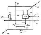
- FIG. 3 illustrates an alternative to the basic multiplier cell described previously ( FIG. 2 ).
- the proposed block is tailored to match the CLC architecture without the addition of any extra hardware (AND gate, etc).
- the functionality demonstrated by the proposed multiplier cell of FIG. 3 is identical to that of the more conventional FIG. 2 .
- the AND gate and Full Adder combination has been replaced by a two input multiplexer 3 . 1 and a Full Adder 3 . 3 .
- the multiplexer 3 . 1 inputs comprise Pi (Partial product in) 3 . 2 and Full Adder out 3 . 4 .
- the Full Adder has the multiplicand bit 3 . 5 , a partial product bit from a previous stage 3 . 2 , and a carry in 3 . 6 from the adjacent CLC incident on its inputs.
- the partial product out 3 . 8 is an input for the next stage and is generated by a multiplier bit 3 . 7 that controls the multiplexer.
- the partial product output 3 . 8 is summation of partial product input 3 . 2 , multiplicand 3 . 5 and carry input 3 . 6 from previous stage while carry out receives Full Adder carryout 3 . 9 .
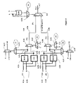
- the multiplier cell topology of FIG. 3 can be mapped to a CLC structure delineated in FIG. 4 .
- the CLC is basically a four input Look Up Table (LUT) with enhanced features for efficient implementation of arithmetic operations.
- LUT Look Up Table
- the CLC in FIG. 4 has the necessary components for implementing any four input function.
- Four of 2 input LUTs 4 . 2 a , 4 . 2 b . 4 . 2 c & 4 . 2 d are coupled via two stage multiplexing.
- the LUTs 4 . 2 are paired and their inputs 4 . 1 a , 4 . 1 b , 4 . 1 c & 4 .
- the paired LUT outputs 4 . 3 a & 4 . 3 b are selected by a first stage two input multiplexer 4 . 4 a controlled by one of the LUT inputs.
- the other paired LUT outputs 4 . 3 c & 4 . 3 d are selected by a first stage two input multiplexer 4 . 4 b controlled by one of the LUT inputs.
- the first stage multiplexers 4 . 4 a & 4 . 4 b outputs 4 . 5 a & 4 . 5 b are directed to a second stage multiplexer 4 .
- Additional multiplexers 4 . 10 , 4 . 11 , 4 . 12 , 4 . 13 , 4 . 14 and 4 . 15 are introduced in the CLC structure to manage addition, subtraction, and multiplication from the CLC without the introduction of any major area or delay overheads.
- the role of these multiplexers will become apparent in the imminent description.
- an addition or subtraction function is not described in detail herein.
- An addition function according to the present invention is disclosed in United States Patent Publication No. 2002/0116426 entitled “Look-Up Table Apparatus To Perform Two-Bit Arithmetic Operation Including Carry Generation” and hereby incorporated by reference.
- a Full Adder should be realizable in the given CLC structure.
- a pair of two input sub LUTs 4 . 2 c & 4 . 2 d can be programmed to function as two input XOR and XNOR gates.
- Xi and Pi signals are applied to the inputs D & C of LUT.
- a multiplexer 4 . 11 is configured to propagate XOR from the sub LUT 4 . 2 c output to a carry generation multiplexer 4 . 10 that selects the previous carry Cin or one of the sub LUT inputs 4 . 1 c as carry in for the next stage.
- the sum F 2 a is selected as an XOR or XNOR of the two inputs Xi and Pi via another multiplexer 4 . 12 .
- an addition or subtraction function is not described in detail herein.
- An addition function according to the present invention is disclosed in United States Patent Publication No. 2002/0116426 entitled “Look-Up Table Apparatus To Perform Two-Bit Arithmetic Operation Including Carry Generation” and hereby incorporated by reference.
- the second part of the multiplier cell of FIG. 3 includes a two input multiplexer 3 . 1 .
- the inputs to this multiplexer are the Full Adder output and the partial product input from the previous stage Pi.
- another pair of sub LUTs 4 . 2 a & 4 . 2 b is configured as a buffer and inverter respectively to an input A of LUT on which input signal Yi is applied.
- the other input B of LUT is treated as don't care type input.
- the buffer configured sub LUT is wired via multiplexer 4 . 14 to control another multiplexer 4 . 15 that puts Yi on the carry chain if Yi equals 0, or else propagates the previous carry to the next stage. Such an arrangement is mandatory as it prevents carry propagation when the multiplicand Yi is zero.
- the partial product from the previous stage Pi is wired via multiplexer 4 . 13 to control another multiplexer 4 . 4 a .
- the net effect is a Pi at the output of 4 . 4 a , when Yi is zero and Pi is desired as the final output.
- the partial product output of the multiplier cell for the next stage is available at the output of multiplexer 4 . 6 that is controlled by Yi via multiplexer 4 . 16 .
- the CLC architecture delineated in FIG. 4 can be configured to accommodate the basic multiplier cell topology.
- a PLD architecture comprising the proposed CLCs can thus accommodate an N bit multiplier in N 2 number of CLCs.
Landscapes
- Physics & Mathematics (AREA)
- General Physics & Mathematics (AREA)
- Engineering & Computer Science (AREA)
- Computational Mathematics (AREA)
- Mathematical Analysis (AREA)
- Mathematical Optimization (AREA)
- Pure & Applied Mathematics (AREA)
- Theoretical Computer Science (AREA)
- Computing Systems (AREA)
- General Engineering & Computer Science (AREA)
- Logic Circuits (AREA)
Abstract
Description
-
- an addition means for adding a first input and a partial product;
- a first multiplexing means for receiving a first output of said addition means at its first input and said partial product at its second input with its select line being controlled by second input, said first multiplexing means providing a first output; and
- a second multiplexing means for receiving a second output of said addition means at its first input and said second input at its second input with its select line being coupled to said second input, said second multiplexing means providing a second output.
-
- adding a first input and a partial product;
- multiplexing a first output of addition means and said partial product depending upon a second input; and
- multiplexing a second output of said addition means and said second input depending upon said second input.
Claims (20)
Applications Claiming Priority (2)
| Application Number | Priority Date | Filing Date | Title |
|---|---|---|---|
| IN2591/DEL/2004 | 2004-12-29 | ||
| IN2591DE2004 | 2004-12-29 |
Publications (2)
| Publication Number | Publication Date |
|---|---|
| US20060195503A1 US20060195503A1 (en) | 2006-08-31 |
| US7856467B2 true US7856467B2 (en) | 2010-12-21 |
Family
ID=36933033
Family Applications (1)
| Application Number | Title | Priority Date | Filing Date |
|---|---|---|---|
| US11/324,019 Active 2029-09-15 US7856467B2 (en) | 2004-12-29 | 2005-12-29 | Integrated circuit including at least one configurable logic cell capable of multiplication |
Country Status (1)
| Country | Link |
|---|---|
| US (1) | US7856467B2 (en) |
Families Citing this family (4)
| Publication number | Priority date | Publication date | Assignee | Title |
|---|---|---|---|---|
| US7279936B2 (en) * | 2003-12-08 | 2007-10-09 | Infineon Technologies Ag | Logic basic cell, logic basic cell arrangement and logic device |
| US9602108B1 (en) * | 2015-09-11 | 2017-03-21 | Xilinx, Inc. | Lut cascading circuit |
| US11374574B2 (en) | 2019-12-27 | 2022-06-28 | Kepler Computing Inc. | Linear input and non-linear output threshold logic gate |
| US12524204B1 (en) * | 2021-09-02 | 2026-01-13 | Kepler Computing Inc. | Ferroelectric or paraelectric based low power multiplier |
Citations (3)
| Publication number | Priority date | Publication date | Assignee | Title |
|---|---|---|---|---|
| US6384627B1 (en) * | 2001-02-16 | 2002-05-07 | Xilinx, Inc. | Logic block used as dynamically configurable logic function |
| US6847228B1 (en) * | 2002-11-19 | 2005-01-25 | Xilinx, Inc. | Carry logic design having simplified timing modeling for a field programmable gate array |
| US7193433B1 (en) * | 2005-06-14 | 2007-03-20 | Xilinx, Inc. | Programmable logic block having lookup table with partial output signal driving carry multiplexer |
-
2005
- 2005-12-29 US US11/324,019 patent/US7856467B2/en active Active
Patent Citations (3)
| Publication number | Priority date | Publication date | Assignee | Title |
|---|---|---|---|---|
| US6384627B1 (en) * | 2001-02-16 | 2002-05-07 | Xilinx, Inc. | Logic block used as dynamically configurable logic function |
| US6847228B1 (en) * | 2002-11-19 | 2005-01-25 | Xilinx, Inc. | Carry logic design having simplified timing modeling for a field programmable gate array |
| US7193433B1 (en) * | 2005-06-14 | 2007-03-20 | Xilinx, Inc. | Programmable logic block having lookup table with partial output signal driving carry multiplexer |
Also Published As
| Publication number | Publication date |
|---|---|
| US20060195503A1 (en) | 2006-08-31 |
Similar Documents
| Publication | Publication Date | Title |
|---|---|---|
| US6066960A (en) | Programmable logic device having combinational logic at inputs to logic elements within logic array blocks | |
| US10613831B2 (en) | Methods and apparatus for performing product series operations in multiplier accumulator blocks | |
| US7660841B2 (en) | Flexible accumulator in digital signal processing circuitry | |
| US5724276A (en) | Logic block structure optimized for sum generation | |
| US11301213B2 (en) | Reduced latency multiplier circuitry for very large numbers | |
| US6288570B1 (en) | Logic structure and circuit for fast carry | |
| EP2391011B1 (en) | A programmable logic device having complex logic blocks with improved logic cell functionality | |
| EP1397863B1 (en) | Reconfigurable logic device | |
| US9292474B1 (en) | Configurable hybrid adder circuitry | |
| US6201409B1 (en) | High performance product term based carry chain scheme | |
| US6603332B2 (en) | Configurable logic block for PLD with logic gate for combining output with another configurable logic block | |
| US10715144B2 (en) | Logic circuits with augmented arithmetic densities | |
| Walters | Partial-product generation and addition for multiplication in FPGAs with 6-input LUTs | |
| US20250103296A1 (en) | Adder circuit using lookup tables | |
| US7617269B2 (en) | Logic entity with two outputs for efficient adder and other macro implementations | |
| US7856467B2 (en) | Integrated circuit including at least one configurable logic cell capable of multiplication | |
| US7167021B1 (en) | Logic device logic modules having improved arithmetic circuitry | |
| US6978427B1 (en) | Literal sharing method for fast sum-of-products logic | |
| Kumar et al. | Reconfigurable delay optimized carry select adder | |
| US20080256165A1 (en) | Full-Adder Modules and Multiplier Devices Using the Same | |
| US7475105B2 (en) | One bit full adder with sum and carry outputs capable of independent functionalities | |
| Sarkar et al. | Low power implementation of multi-bit hybrid adder using modified GDI technique | |
| US7176715B1 (en) | Computer combinatorial multipliers in programmable logic devices | |
| US6844756B1 (en) | Configurable dedicated logic in PLDs | |
| Sworna et al. | An Efficient Design of an FPGA-Based Multiplier Using LUT Merging Theorem |
Legal Events
| Date | Code | Title | Description |
|---|---|---|---|
| AS | Assignment |
Owner name: STMICROELECTRONICS PVT. LTD., INDIA Free format text: ASSIGNMENT OF ASSIGNORS INTEREST;ASSIGNORS:SWAMI, PARVESH;BAL, ANKUR;REEL/FRAME:017878/0047;SIGNING DATES FROM 20060208 TO 20060209 Owner name: STMICROELECTRONICS PVT. LTD., INDIA Free format text: ASSIGNMENT OF ASSIGNORS INTEREST;ASSIGNORS:SWAMI, PARVESH;BAL, ANKUR;SIGNING DATES FROM 20060208 TO 20060209;REEL/FRAME:017878/0047 |
|
| STCF | Information on status: patent grant |
Free format text: PATENTED CASE |
|
| FPAY | Fee payment |
Year of fee payment: 4 |
|
| MAFP | Maintenance fee payment |
Free format text: PAYMENT OF MAINTENANCE FEE, 8TH YEAR, LARGE ENTITY (ORIGINAL EVENT CODE: M1552) Year of fee payment: 8 |
|
| MAFP | Maintenance fee payment |
Free format text: PAYMENT OF MAINTENANCE FEE, 12TH YEAR, LARGE ENTITY (ORIGINAL EVENT CODE: M1553); ENTITY STATUS OF PATENT OWNER: LARGE ENTITY Year of fee payment: 12 |