US7817763B2 - Processing method for providing, starting from signals acquired by a set of sensors, an aggregate signal and data acquisition system using such method - Google Patents
Processing method for providing, starting from signals acquired by a set of sensors, an aggregate signal and data acquisition system using such method Download PDFInfo
- Publication number
- US7817763B2 US7817763B2 US11/787,194 US78719407A US7817763B2 US 7817763 B2 US7817763 B2 US 7817763B2 US 78719407 A US78719407 A US 78719407A US 7817763 B2 US7817763 B2 US 7817763B2
- Authority
- US
- United States
- Prior art keywords
- data
- signal
- processing unit
- signals
- format
- Prior art date
- Legal status (The legal status is an assumption and is not a legal conclusion. Google has not performed a legal analysis and makes no representation as to the accuracy of the status listed.)
- Active, expires
Links
Images


Classifications
-
- H—ELECTRICITY
- H04—ELECTRIC COMMUNICATION TECHNIQUE
- H04L—TRANSMISSION OF DIGITAL INFORMATION, e.g. TELEGRAPHIC COMMUNICATION
- H04L12/00—Data switching networks
- H04L12/28—Data switching networks characterised by path configuration, e.g. LAN [Local Area Networks] or WAN [Wide Area Networks]
- H04L12/2854—Wide area networks, e.g. public data networks
- H04L12/2856—Access arrangements, e.g. Internet access
Definitions
- An embodiment of the present invention relates to data acquisition, processing, and transmission, and in particular is concerned with a processing method for providing an aggregate signal, starting from signals acquired from a set of sensors.
- An embodiment of the present invention further relates to a data-acquisition system using such method.
- the use of sensor networks has proven itself particularly advantageous in the security-systems field, in bio-medical applications, in the environment-control field, and in the transport field.
- the sensor networks used are wireless networks, often referred to by the WSN acronym (Wireless Sensors Network).
- a transmission technique that envisages grouping the sensors provided for acquiring data concerning homogeneous quantities, in such a way as to form groups of sensors.
- Each of such groups is associated with a local processing unit (that, generally, may be integrated in a sensor of the group), provided for receiving signals output by the sensors, processing such signals to form an aggregate signal, and transmitting such aggregate signal to the remote processing unit.
- the local processing unit generally comprises a micro-controller with very low power dissipation (MCU, Ultra-low-power Micro Controller) adapted to execute the above described operations.
- the aggregate signal is obtained from the local processing unit by a merge (also referred to in the field by the word “beamforming”) of signals output by various sensors of the group, exploiting the redundancy present in such signals.
- a merge also referred to in the field by the word “beamforming”
- such merge is obtained by adaptive equalization.
- the merge is obtained by a Kalman filtering.
- An embodiment of the present invention makes available a signal processing method, or a beamforming method, for provide an aggregate signal from a plurality of starting signals and that overcomes one or more of the above-described shortcomings.
- FIG. 1 shows an exemplary block diagram of a data-acquisition system according to an embodiment of the present invention, comprising a sensors network, a local processing unit and a remote processing unit.
- FIG. 2 shows an exemplary block diagram of the local processing unit of FIG. 1 .
- FIG. 3 shows an exemplary logic scheme of a swap module of the local processing unit of FIG. 2 .
- FIG. 4 shows an exemplary block diagram of the remote processing unit of FIG. 1 .
- FIG. 5 shows a waveform portion of an exemplary output signal provided by a sensor and a waveform portion of a signal extracted from the aggregate signal.
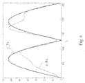
- FIGS. 6 and 7 each show a waveform section of an exemplary output signal provided by a sensor and a waveform section of the signal extracted from the aggregate signal following a filtering operation.
- FIG. 8 shows waveforms of exemplary output signals provided by a group of four sensors and corresponding signals extracted from an aggregate signal y beam .
- FIG. 1 is schematically shown an example of a data acquisition system, generally indicated at 1 , comprising a sensor network 2 , a local processing unit L_PU and a remote processing unit R_PU.
- Sensor network 2 comprises a plurality of sensors U 1 , . . . , U 5 , for instance micro-sensors (MEMS), that together forms a set of homogeneous sensors U 1 , . . . , U 5 .
- the term “homogeneous group” of sensors U 1 , . . . , U 5 means a group of sensors adapted to measure the same physical quantity to provide in output a respective acquired signal x 1 , . . . , x 5 representing such physical quantity.
- sensors U 1 , . . . , U 5 might all be sensors adapted to measure a respective value of room temperature.
- sensors U 1 , . . . , U 5 might all be sensors adapted to measure a respective value of a same chemical quantity.
- a sensor network 2 has been schematically shown comprising five sensors U 1 , . . . , U 5 , the network 2 may include any integer number of sensors at least equal to two.
- Each sensor U 1 , . . . , U 5 comprises one or more transducers for acquiring signals x 1 , . . . , x 5 , representative of the measured physical quantity, and comprises further resources for generating and transmitting such signal x 1 , . . . , x 5 processing and output transmission. More specifically, each sensor U 1 , . . . , U 5 comprises analog/digital conversion means, to provide in output said signals x 1 , . . . , x 5 as digital signals, that is comprising data in a digital format and having a resolution of N res bits.
- signals x 1 , . . . , x 5 output from sensors network 2 are analog signals destined to be converted in digital signals by suitable analog/digital conversion means provided in the local processing unit L_PU.
- Sensors network 2 comprises a local processing unit L_PU which preferably, as in the example illustrated in FIG. 1 , is integrated in one of said network 2 sensors, in the shown example in sensor U 5 .
- local processing unit L_PU could be separate from each of the sensors U 1 , . . . , U 5 of the sensors network 2 .
- Local processing unit L_PU is such to receive different digital signals x 1 , . . . , x 5 acquired and provided in output from network 2 sensors U 1 , . . . , U 5 .
- Local processing unit L_PU comprises processing means for processing digital signals x 1 , . . . , x 5 provided from sensors U 1 , . . . , U 5 and to form, starting from such signals, an aggregate digital signal y beam to be transmitted to the remote processing unit R_PU.
- Local processing unit L_PU comprises processing means in the form of a low-dissipation micro-controller.
- sensor network 2 and more generally data-acquisition system 1
- data transmission among different entities constituting network 2 takes place by free space propagation of radio frequency signals.
- such transmission might take place via wired connections between at least some of different network/system entities.
- each signal x 1 , . . . , x 5 a dedicated frequency channel (FDMA) or as, an alternative, envisage a time-sharing multiple access (TDMA) of different signals x 1 , . . . , x 5 to a single channel (TDMA), or even envisage a mixed system FDMA/TDMA.
- FDMA dedicated frequency channel
- TDMA time-sharing multiple access
- FIG. 2 is shown a block diagram of an embodiment of local processing unit L_PU, in this example integrated in one of the homogeneous sensors U 1 , . . . , U 5 set.
- Local processing unit L_PU is such to receive input digital signals x 1 , . . . , x 5 provided from the sensors and comprises processing means B swap , B form for forming an aggregate signal Y beam .
- Processing means B swap , B form comprise a swap block B swap adapted to modify signals x 1 , . . . , x 5 received in input exchanging the data format of each of said signals from a first format to a second format.
- x 1 (t) . . . , x 5 (t) are indicated at clock cycle t digital data in the first format of signals x 1 , . . . , x 5
- xs 1 (t), . . . , xs 5 (t) are indicated at clock cycle t digital data in the second format of signals xs 1 , . . . , xs 5 .
- Each data xs 1 (t), . . . , xs 5 (t) in the second format is obtained from a respective data in the first format x 1 (t), . . . , x 5 (t) by a permutation operation such as to change the bit positions within each data based upon a permutation scheme p 1 (t), . . . , p 5 (t) associated with data x 1 (t), . . . , x 5 (t) and with the specific digital signal x 1 , . . . , x 5 comprising such data x 1 (t), . . . , x 5 (t).
- a permutation operation such as to change the bit positions within each data based upon a permutation scheme p 1 (t), . . . , p 5 (t) associated with data x 1 (t), . . . , x 5 (t) and with the specific digital signal x 1
- the permutation schemes p 1 (t), . . . , p 5 (t) may be selected by the remote processing unit R_PU and transmitted to the local processing unit L_PU trough at least one signal P .
- swap block B swap has been shown as formed by a plurality of swap modules B s1 , B s2 , B s3 , B s4 , B s5 , each assigned to process a respective input signal x 1 , . . . , x 5 .
- swap block B swap may be implemented through a single processing unit shared among all signals x 1 , . . . , x 5 .
- FIG. 3 is shown an example of the logic scheme of a swap module, and particularly of swap module B s1 provided for processing signal x 1 .
- the permutation scheme (indicated as p 1 in FIG. 3 ) may be in turn expressed as a data, or a coded word, that may take up to N res ! values, each may be represented with N res digits, or each may be represented with n bits.
- swap module B s1 performs a bit permutation such that:
- positional bitwise logic operators are the following: AND, NAND, OR, NOR, EX-NOR, etc. . . . or any combination of said operators.
- input signal data x 1 , . . . , x 5 to be modified from the swap block B swap and, more particularly, swap units B s1 , B s2 , B s3 , B s4 , B s5 , are represented by a considerable number of bits (for instance 16), one may realize the swap operation such that it operates rigidly on M blocks of input data bits, wherein M is a greater than 1 integer, overall such as envisaged from the teachings of the above mentioned US patent application 2004/0201505 A1. This allows, as will be explained better in the following, a reduction in the permutation schemes' p 1 (t), . . .
- any permutation schemes may be selected within a set of N res ! (factorial) possible permutation schemes, while in the case wherein one operates upon M groups of bits this may be selected among M! (factorial) possible permutation schemes. This allows one to reduce considerably computational complexity at the remote processing unit R_PU of the permutation schemes to be utilized by the local processing unit.
- each of the input signals to the swap block B swap shows stationarity characteristics (for example strict stationarity)
- stationarity characteristics for example strict stationarity
- each x 1 , . . . , x 5 input signal a dedicated permutation scheme group (or set) comprising a finite number W of permutation schemes to be utilized cyclically (i.e., repeatedly), for instance sequentially, for modifying the data format of said input signal.
- x 1 , . . . , x 5 input signals present modest stationarity characteristics, it is possible to envisage for each said x 1 , . . .
- x 5 signals an update of said sets of permutation schemes by the remote processing unit R_PU with an update frequency, for example, much lower compared to the clock frequency of signals x 1 , . . . , x 5 received in input to the swap block B swap .
- processing means B swap and B form of local processing unit L_PU further comprise an aggregation (beamforming) block B form for producing starting from signals xs 1 (t), . . . , xs 5 (t) as processed by swap block B swap an aggregate signal y beam (t) having N res bits resolution data.
- aggregation (beamforming) block B form for producing starting from signals xs 1 (t), . . . , xs 5 (t) as processed by swap block B swap an aggregate signal y beam (t) having N res bits resolution data.
- Aggregation block B form produces such aggregate signal y beam by applying a positional logic operator bitwise O pl upon corresponding bits of signals xs 1 (t), . . . , xs 5 (t) for producing a single bit of the aggregate signal y beam .
- the positional logic operator O pl is the Boolean operator EX-OR (also called exclusive OR, also represented by symbol ⁇ ).
- aggregation block B form produces the i-th bit of aggregate signal y beam (t) at clock cycle t by computing:
- the aggregate signal y beam (t) data at clock cycle t maybe written in the form:
- y beam ⁇ ( t ) ⁇ ⁇ u ⁇ S ⁇ [ x u ⁇ ( t ) , p u ⁇ ( t ) ] ( 7 )
- p u (t) is the permutation scheme assigned at clock cycle t to digital signal x u (t) to modify said data format through swap block B swap .
- permutation schemes p u (t) that represent in practice digital signatures for the same signal x u may be repeated cyclically as clock t cycles vary.
- permutation sequences p u (t) may be used to apply to the same signal from a set (associated with said signal) comprising a finite number W of possible sequences identified by the remote processing unit R_PU to modify, in practice to “sign”, said signal. More generally, using a bitwise positional logic operator O pl in the aggregation block B form one has:
- local processing unit L_PU is such as to send aggregate signal y beam thus obtained to remote processing unit R_PU using a digital modulation, such as for instance a QPSK modulation or a B-PSK modulation compliant with the IEEE 802.14.5 standard.
- a digital modulation such as for instance a QPSK modulation or a B-PSK modulation compliant with the IEEE 802.14.5 standard.
- Remote processing unit R_PU is such as to receive said aggregate signal y beam to decode it with the aim of extracting (that is detect) from it single signals x 1 , . . . , x 5 supplied in output by sensors U 1 , . . . , U 5 of sensors network 2 , or more correctly, of extracting from y beam an as-accurate-as-possible estimate of such x 1 , . . . , x 5 signals.
- an “estimate as accurate as possible” is meant an estimate having an accuracy level compatible with some predefined system requirements.
- FIG. 4 is shown an exemplary block diagram of an embodiment of a remote processing unit R_PU.
- Such remote processing unit R_PU comprises a reverse swap block B swap ⁇ 1 similar to the above described swap block referring to the local processing unit L_PU and to FIG. 2 .
- reverse swap block B swap ⁇ 1 has been represented as comprising a plurality of reverse swap blocks B s1 ⁇ 1 , . . . , B s5 ⁇ 1 each provided for processing the aggregate signal y beam for reconstructing a respective signal x 1 , . . . , x 5 provided in output from sensors U 1 , . . . , U 5 and transmitted to local processing unit L_PU.
- reverse swap block B swap ⁇ 1 operates in such a way to process the aggregate signal y beam by applying to said signal data-swap operators that use reverse permutation schemes p 1 ⁇ 1 , . . . , p 5 ⁇ 1 with respect to permutation schemes p 1 , . . . , p 5 used by swap block B swap in local processing unit L_PU.
- the remote processing unit R_PU comprises a search block P search provided for searching permutation schemes, or better sets (or sequences) comprising a limited and restricted number W of permutation schemes, to be transmitted to the local processing unit L_PU with the aim of reducing as far as possible, from each u-th signal to be extracted (i.e., to be revealed) from aggregate signal y beam , the interference due to the process w u (t).
- w u ⁇ ( t ) ⁇ ⁇ ⁇ m ⁇ u ⁇ S ⁇ [ S ⁇ [ x m ⁇ ( t ) , p m ⁇ ( t ) ] , p u - 1 ⁇ ( t ) ] ⁇ ⁇ ⁇ ( 10 )
- ⁇ is an arbitrary small predefined value. The above criteria correspond to minimize noise energy E u due to w u (t) process.
- the U permutation sequences sets search according to above-noted criteria has a computational complexity that reduces itself to (M!) U ⁇ W .
- the permutation schemes sequences search problem may be solved in a heuristic way, through the study of the characteristics of the signals provided in output from sensors U 1 , . . . , U 5 such as to minimize the noise spectral density of w u (n).
- search block P search executes the permutation-sequence-schemes search operation in a sub-optimal way minimizing (or maximizing) a predefined cost function, that represents the search operation metric and that is given by the sum (or by the product, using logarithms) of an individual contribution plurality.
- search block P search operates according to a Viterbi algorithm.
- search block P search realizes a Viterbi algorithm according to the following operations:
- An embodiment of a Viterbi algorithm carried out by search block P search uses a fully connected trellis diagram. This means that in the Viterbi algorithm, once a selected permutation scheme (start state) starts at cycle t-1, it is possible to carry out a transition (that is carry out a trial) at cycle t towards any permutation scheme (arrival state) including the start one.
- This selection compared to the use of a partially connected trellis, does not limit the system's degrees of freedom during the permutation schemes sets search.
- adopting a partially connected trellis scheme may be a strategy to be used to reduce the number of trials to be carried out during the permutation schemes sequence.
- remote processing unit R_PU besides the search operations of permutation schemes sequences and of extraction of different signals from the aggregate signal, carries out post-processing operations on extracted signals.
- extracted signals from aggregate signal y beam may show replicas in the time domain (due to frequency domain sampling) and high-frequency components that require a base-band conversion and a subsequent low-pass-type filtering.
- filtering may be carried out by a Butterworth filter or an elliptic type filter (not shown in FIG. 4 scheme).
- FIG. 5 is shown the time pattern of a signal provided in output by one of the sensors (indicated as x-Tx) and of the corresponding signal (indicated as x_Rx) extracted by the remote processing unit R_PU from the aggregate signal.
- extracted signal x_Rx shows high frequency components.
- signal x_Tx is compared with extracted signal x_Rx following a filtering operation by an 8-pole low-pass Butterworth filter with a normalized frequency of 0.000025 Hz.
- transmitted signal x_Tx is compared with extracted signal x_Rx after a filtering operation by an elliptic two-pole low-pass filter having a normalized frequency equal to 0.025 Hz.
- FIG. 8 four signals are shown x 1 , . . . , x 4 provided in output from four sensors U 1 , . . . , U 4 (of a four-sensor group) and corresponding signals x 1— Rx, . . . , x 4— Rx extracted from aggregate signal y beam , filtered and detected.
- the sensor group 2 of FIG. 1 may be disposed on an integrated circuit (IC) that may be part of a first system and coupled to another IC such as a processor/controller.
- IC integrated circuit
- the remote processor R_PU may by formed on the same or a different IC, and this IC may be part of the first or part of a second system, and coupled to another IC such as a processor/controller.
Abstract
-
- acquiring said starting signals through respective sensors of a homogeneous sensors group;
- converting acquired signals in respective digital signals having data represented with a predetermined bits number;
- processing the digital signals to form aggregate signal.
-
- modifying digital signals changing the data format of each such digital signals from a first format to a second format, each data in the second format having been obtained from a respective data in the first format through an operation of permuting the bits position according to a permutation scheme associated with said data and to the specific digital signal comprising that data;
- forming aggregate signal obtaining said aggregate signal data by means of a bitwise logic operator acting upon said modified digital signal respective data.
Description
-
- the
bit having position 0 in the input data hasposition 2 bit in the output data; - the
bit having position 1 in the input data hasposition 3 bit in the output data; - the
bit having position 2 in the input data hasposition 0 bit in the output data; and - the
bit having position 3 in the input data hasposition 1 bit in the output data;
- the
B s1(t)=S[x 1(t), p 1(t)]=Xs 1(t). (1)
x 1(t)=S −1 [xs 1(t), p 1(t)]=S[xs 1(t), p −1(t)]. (2)
| p1 | p−1 | ||
| 1, 2, 3, 0 | 3, 0, 1, 2 | ||
| 1, 0, 2, 3 | 1, 0, 2, 3 | ||
| 2, 1, 3, 0 | 3, 1, 0, 2 | ||
| 1, 3, 0, 2 | 2, 0, 3, 1 | ||
wherein p(t) represents any swap sequence.
wherein p(t) represents any swap sequence.
y beam(t)=O pl [xs 1(t), . . . , xs 5(t)]. (5).
wherein pu(t) is the permutation scheme assigned at clock cycle t to digital signal xu(t) to modify said data format through swap block Bswap. As previously explained, permutation schemes pu(t) that represent in practice digital signatures for the same signal xu may be repeated cyclically as clock t cycles vary. In that way, permutation sequences pu(t) may be used to apply to the same signal from a set (associated with said signal) comprising a finite number W of possible sequences identified by the remote processing unit R_PU to modify, in practice to “sign”, said signal. More generally, using a bitwise positional logic operator Opl in the aggregation block Bform one has:
wherein ε is an arbitrary small predefined value. The above criteria correspond to minimize noise energy Eu due to wu(t) process. Such energy Eu is given by:
E u=Σi=0 N
wherein wu(t)(0) is the signal wu(t) least-significant bit while wu(t)(Nres−1) is the signal wu(t) most-significant bit.
-
- a) casually generate a permutation schemes sequence (in practice, comprising W schemes) to be associated with first x1 of U signals provided in output from sensors, and
-
- b) identify, operating signal by signal and through trials, respective permutation schemes sequences, such as to minimize for each (remaining) signal xu a given cost function (or metric) of energy Eu (substantially as defined in formula 10) of interference (substantially as defined in formula 9) of the other signals whose permutation schemes have already been identified through Viterbi algorithm.
Claims (18)
Priority Applications (2)
| Application Number | Priority Date | Filing Date | Title |
|---|---|---|---|
| US12/844,460 US8817935B2 (en) | 2006-04-12 | 2010-07-27 | Processing method for providing, starting from signals acquired by a set of sensors, an aggregate signal and data acquisition system using such method |
| US12/844,451 US8126084B2 (en) | 2006-04-12 | 2010-07-27 | Processing method for providing, starting from signals acquired by a set of sensors, an aggregate signal and data acquisition system using such method |
Applications Claiming Priority (3)
| Application Number | Priority Date | Filing Date | Title |
|---|---|---|---|
| EP06425259A EP1845660B1 (en) | 2006-04-12 | 2006-04-12 | Method for aggregating and transmitting sensor signals |
| EP06425259.6 | 2006-04-12 | ||
| EP06425259 | 2006-04-12 |
Related Child Applications (2)
| Application Number | Title | Priority Date | Filing Date |
|---|---|---|---|
| US12/844,451 Division US8126084B2 (en) | 2006-04-12 | 2010-07-27 | Processing method for providing, starting from signals acquired by a set of sensors, an aggregate signal and data acquisition system using such method |
| US12/844,460 Division US8817935B2 (en) | 2006-04-12 | 2010-07-27 | Processing method for providing, starting from signals acquired by a set of sensors, an aggregate signal and data acquisition system using such method |
Publications (2)
| Publication Number | Publication Date |
|---|---|
| US20080037667A1 US20080037667A1 (en) | 2008-02-14 |
| US7817763B2 true US7817763B2 (en) | 2010-10-19 |
Family
ID=36685657
Family Applications (3)
| Application Number | Title | Priority Date | Filing Date |
|---|---|---|---|
| US11/787,194 Active 2029-06-18 US7817763B2 (en) | 2006-04-12 | 2007-04-12 | Processing method for providing, starting from signals acquired by a set of sensors, an aggregate signal and data acquisition system using such method |
| US12/844,460 Active 2027-10-20 US8817935B2 (en) | 2006-04-12 | 2010-07-27 | Processing method for providing, starting from signals acquired by a set of sensors, an aggregate signal and data acquisition system using such method |
| US12/844,451 Active US8126084B2 (en) | 2006-04-12 | 2010-07-27 | Processing method for providing, starting from signals acquired by a set of sensors, an aggregate signal and data acquisition system using such method |
Family Applications After (2)
| Application Number | Title | Priority Date | Filing Date |
|---|---|---|---|
| US12/844,460 Active 2027-10-20 US8817935B2 (en) | 2006-04-12 | 2010-07-27 | Processing method for providing, starting from signals acquired by a set of sensors, an aggregate signal and data acquisition system using such method |
| US12/844,451 Active US8126084B2 (en) | 2006-04-12 | 2010-07-27 | Processing method for providing, starting from signals acquired by a set of sensors, an aggregate signal and data acquisition system using such method |
Country Status (2)
| Country | Link |
|---|---|
| US (3) | US7817763B2 (en) |
| EP (1) | EP1845660B1 (en) |
Cited By (1)
| Publication number | Priority date | Publication date | Assignee | Title |
|---|---|---|---|---|
| US20100289628A1 (en) * | 2006-04-12 | 2010-11-18 | STMicroelectronics,S.r.l. | Processing method for providing, starting from signals acquired by a set of sensors, an aggregate signal and data acquisition system using such method |
Families Citing this family (2)
| Publication number | Priority date | Publication date | Assignee | Title |
|---|---|---|---|---|
| WO2010092435A1 (en) * | 2009-02-11 | 2010-08-19 | Nokia Corporation | Method, apparatus, and computer program product for collaborative network communications |
| IT1400096B1 (en) | 2010-05-12 | 2013-05-17 | St Microelectronics Srl | PROCESS OF MANUFACTURE OF INTEGRATED ELECTRONIC CIRCUITS AND CIRCUITS OBTAINED SO |
Citations (4)
| Publication number | Priority date | Publication date | Assignee | Title |
|---|---|---|---|---|
| US20040026510A1 (en) | 2002-08-07 | 2004-02-12 | Shenzhen Syscan Technology Co., Limited. | Methods and systems for encoding and decoding data in 2D symbology |
| US20050210340A1 (en) * | 2004-03-18 | 2005-09-22 | Townsend Christopher P | Wireless sensor system |
| US7002470B1 (en) * | 2004-05-03 | 2006-02-21 | Miao George J | Wireless UWB-based space-time sensor networks communications |
| US7456770B2 (en) * | 2007-03-02 | 2008-11-25 | Telefonaktiebolaget I.M. Ericsson (Publ) | Distributed sigma-delta sensor network |
Family Cites Families (8)
| Publication number | Priority date | Publication date | Assignee | Title |
|---|---|---|---|---|
| US6381726B1 (en) * | 1999-01-04 | 2002-04-30 | Maxtor Corporation | Architecture for soft decision decoding of linear block error correcting codes |
| US6877043B2 (en) * | 2000-04-07 | 2005-04-05 | Broadcom Corporation | Method for distributing sets of collision resolution parameters in a frame-based communications network |
| US7242726B2 (en) * | 2000-09-12 | 2007-07-10 | Broadcom Corporation | Parallel concatenated code with soft-in soft-out interactive turbo decoder |
| EP1380961B1 (en) * | 2002-07-10 | 2006-04-05 | STMicroelectronics S.r.l. | Process and device for reducing bus switching activity and computer program product therefor |
| GB2399722A (en) * | 2003-03-21 | 2004-09-22 | Sony Uk Ltd | Data communication synchronisation |
| FR2860360B1 (en) * | 2003-09-29 | 2005-12-09 | Canon Kk | ENCODING / DECODING DEVICE USING REED-SOLOMON ENCODER / DECODER |
| FR2863794B1 (en) * | 2003-12-16 | 2006-03-03 | Canon Kk | ERROR LOCATION METHODS AND DEVICES FOR ALGEBRA GEOMETRY CODES |
| EP1845660B1 (en) * | 2006-04-12 | 2012-08-29 | STMicroelectronics Srl | Method for aggregating and transmitting sensor signals |
-
2006
- 2006-04-12 EP EP06425259A patent/EP1845660B1/en active Active
-
2007
- 2007-04-12 US US11/787,194 patent/US7817763B2/en active Active
-
2010
- 2010-07-27 US US12/844,460 patent/US8817935B2/en active Active
- 2010-07-27 US US12/844,451 patent/US8126084B2/en active Active
Patent Citations (4)
| Publication number | Priority date | Publication date | Assignee | Title |
|---|---|---|---|---|
| US20040026510A1 (en) | 2002-08-07 | 2004-02-12 | Shenzhen Syscan Technology Co., Limited. | Methods and systems for encoding and decoding data in 2D symbology |
| US20050210340A1 (en) * | 2004-03-18 | 2005-09-22 | Townsend Christopher P | Wireless sensor system |
| US7002470B1 (en) * | 2004-05-03 | 2006-02-21 | Miao George J | Wireless UWB-based space-time sensor networks communications |
| US7456770B2 (en) * | 2007-03-02 | 2008-11-25 | Telefonaktiebolaget I.M. Ericsson (Publ) | Distributed sigma-delta sensor network |
Non-Patent Citations (4)
| Title |
|---|
| A. Wang, W. Einzelam, and A. P. Chandrakasan, "Energy Scalable Protocols for Battery-Operated MicroSensor Network", Kluwer Journal of VLSI Signal Processing, pp. 223-239, Nov. 2001. |
| European Search Report for EP 06 42 5259 dated Sep. 1, 2006. |
| Heinzelman W R et al., "Energy-scalable algorithms and protocols for wireless microsensor networks", Acoustics, Speech, and Signal Processing, 2000. ICASSP '00. Proceedings. 2000 IEEE International Conference on Jun. 5-9, 2000, Piscataway, NJ, USA, IEEE, vol. 6, Jun. 5, 2000, pp. 3722-3725, XP010505707. |
| Sinha A et al., "Algorithmic transforms for efficient energy scalable computation", Low Power Electronics and Design, 2000, ISLPED '00, Proceedings of the 2000 International Symposium on Jul. 26-27, 2000, Piscataway, NJ, USA, IEEE, Jul. 26, 2000, pp. 31-36, XP010517300. |
Cited By (2)
| Publication number | Priority date | Publication date | Assignee | Title |
|---|---|---|---|---|
| US20100289628A1 (en) * | 2006-04-12 | 2010-11-18 | STMicroelectronics,S.r.l. | Processing method for providing, starting from signals acquired by a set of sensors, an aggregate signal and data acquisition system using such method |
| US8817935B2 (en) | 2006-04-12 | 2014-08-26 | Stmicroelectronics S.R.L. | Processing method for providing, starting from signals acquired by a set of sensors, an aggregate signal and data acquisition system using such method |
Also Published As
| Publication number | Publication date |
|---|---|
| EP1845660A1 (en) | 2007-10-17 |
| US8817935B2 (en) | 2014-08-26 |
| US20080037667A1 (en) | 2008-02-14 |
| EP1845660B1 (en) | 2012-08-29 |
| US20100290567A1 (en) | 2010-11-18 |
| US20100289628A1 (en) | 2010-11-18 |
| US8126084B2 (en) | 2012-02-28 |
Similar Documents
| Publication | Publication Date | Title |
|---|---|---|
| CN1791120B (en) | System and method for effectively aligning data bit of parallel data channel | |
| CN110008166B (en) | Orthogonal differential vector signaling code with embedded clock | |
| CN101401346B (en) | Method and apparatus for transmitting a packet in a wireless communications network | |
| US6741193B2 (en) | Parallel in serial out circuit having flip-flop latching at multiple clock rates | |
| CN106100789B (en) | Multilayer MIMO wireless sensor network blind checking method based on sub-clustering | |
| CN106063181B (en) | Receiver circuit and the method operated on receiver circuit | |
| US7817763B2 (en) | Processing method for providing, starting from signals acquired by a set of sensors, an aggregate signal and data acquisition system using such method | |
| Kumar et al. | A survey on NOMA techniques for 5G scenario | |
| Muzaffar et al. | A pulsed-index technique for single-channel, low-power, dynamic signaling | |
| CN105224485B (en) | A kind of method of reseptance and device of pervasive serial data | |
| Bhatnagar et al. | An FPGA software defined radio platform with a high-level synthesis design flow | |
| JP2001352318A (en) | Transmission circuit and its method, reception circuit and its method, and data communication equipment | |
| CN103441966B (en) | Distributed MIMO frequency deviation and channel estimation based on ECM under a kind of high speed | |
| Zhou et al. | New families of optimal zero correlation zone sequences based on interleaved technique and perfect sequences | |
| Ahmed et al. | Overloaded CDMA bus topology for MPSoC interconnect | |
| EP1538791A2 (en) | Data communication | |
| Jalan et al. | Symbolic synchronization and the detection of global properties of coupled dynamics from local information | |
| RU2284655C1 (en) | Parallel counter of singular signals | |
| CN101149763B (en) | Burst mode asynchronous control circuit design method | |
| Vijayalakshmi et al. | A design of body channel communication transceiver using Manchester decoder for high-speed applications | |
| CN101232350B (en) | Parity error detecting circuit | |
| CN109831192A (en) | For conveyer, the physical layer circuit of receiver and its method and communication system | |
| Dogaru | HCA101: A chaotic map based on cellular automata with binary synchronization properties | |
| JP2011146974A (en) | Radio communication method and system, radio communication apparatus, and program | |
| US7346099B2 (en) | Network fabric physical layer |
Legal Events
| Date | Code | Title | Description |
|---|---|---|---|
| AS | Assignment |
Owner name: STMICROELECTRONICS S.R.L., ITALY Free format text: ASSIGNMENT OF ASSIGNORS INTEREST;ASSIGNORS:VISALLI, GIUSEPPE;PAPPALARDO, FRANCESCO;REEL/FRAME:019553/0629 Effective date: 20070402 |
|
| STCF | Information on status: patent grant |
Free format text: PATENTED CASE |
|
| FPAY | Fee payment |
Year of fee payment: 4 |
|
| MAFP | Maintenance fee payment |
Free format text: PAYMENT OF MAINTENANCE FEE, 8TH YEAR, LARGE ENTITY (ORIGINAL EVENT CODE: M1552) Year of fee payment: 8 |
|
| MAFP | Maintenance fee payment |
Free format text: PAYMENT OF MAINTENANCE FEE, 12TH YEAR, LARGE ENTITY (ORIGINAL EVENT CODE: M1553); ENTITY STATUS OF PATENT OWNER: LARGE ENTITY Year of fee payment: 12 |