US7809346B2 - Digital audio receiver with reduced AM interference - Google Patents
Digital audio receiver with reduced AM interference Download PDFInfo
- Publication number
- US7809346B2 US7809346B2 US11/118,831 US11883105A US7809346B2 US 7809346 B2 US7809346 B2 US 7809346B2 US 11883105 A US11883105 A US 11883105A US 7809346 B2 US7809346 B2 US 7809346B2
- Authority
- US
- United States
- Prior art keywords
- frequency
- sample rate
- frame rate
- signal
- pwm
- Prior art date
- Legal status (The legal status is an assumption and is not a legal conclusion. Google has not performed a legal analysis and makes no representation as to the accuracy of the status listed.)
- Active, expires
Links
- 238000005070 sampling Methods 0.000 claims abstract description 90
- 238000000034 method Methods 0.000 claims description 32
- 238000012545 processing Methods 0.000 claims description 23
- 230000005236 sound signal Effects 0.000 claims description 22
- 238000012952 Resampling Methods 0.000 claims description 5
- 230000000737 periodic effect Effects 0.000 claims description 4
- 238000006243 chemical reaction Methods 0.000 abstract description 56
- 230000006870 function Effects 0.000 description 33
- 230000008569 process Effects 0.000 description 22
- 101000885321 Homo sapiens Serine/threonine-protein kinase DCLK1 Proteins 0.000 description 17
- 102100039758 Serine/threonine-protein kinase DCLK1 Human genes 0.000 description 17
- 230000004044 response Effects 0.000 description 14
- 238000010586 diagram Methods 0.000 description 10
- 238000010276 construction Methods 0.000 description 9
- 238000001914 filtration Methods 0.000 description 9
- 238000012360 testing method Methods 0.000 description 9
- 238000004519 manufacturing process Methods 0.000 description 7
- 230000008901 benefit Effects 0.000 description 5
- 229920000729 poly(L-lysine) polymer Polymers 0.000 description 5
- 238000013459 approach Methods 0.000 description 4
- 230000000694 effects Effects 0.000 description 4
- 230000035945 sensitivity Effects 0.000 description 4
- 238000012986 modification Methods 0.000 description 3
- 230000004048 modification Effects 0.000 description 3
- 238000007493 shaping process Methods 0.000 description 3
- 230000009286 beneficial effect Effects 0.000 description 2
- 230000000295 complement effect Effects 0.000 description 2
- 238000007796 conventional method Methods 0.000 description 2
- 238000001514 detection method Methods 0.000 description 2
- 230000010354 integration Effects 0.000 description 2
- 101100063435 Caenorhabditis elegans din-1 gene Proteins 0.000 description 1
- BNPSSFBOAGDEEL-UHFFFAOYSA-N albuterol sulfate Chemical class OS(O)(=O)=O.CC(C)(C)NCC(O)C1=CC=C(O)C(CO)=C1.CC(C)(C)NCC(O)C1=CC=C(O)C(CO)=C1 BNPSSFBOAGDEEL-UHFFFAOYSA-N 0.000 description 1
- 230000003321 amplification Effects 0.000 description 1
- 230000015572 biosynthetic process Effects 0.000 description 1
- 230000008859 change Effects 0.000 description 1
- 238000012512 characterization method Methods 0.000 description 1
- 230000006835 compression Effects 0.000 description 1
- 238000007906 compression Methods 0.000 description 1
- 238000012937 correction Methods 0.000 description 1
- 238000011161 development Methods 0.000 description 1
- 230000006872 improvement Effects 0.000 description 1
- 238000003199 nucleic acid amplification method Methods 0.000 description 1
- 239000002243 precursor Substances 0.000 description 1
- 230000009467 reduction Effects 0.000 description 1
- 238000011160 research Methods 0.000 description 1
- 230000000630 rising effect Effects 0.000 description 1
- 239000004065 semiconductor Substances 0.000 description 1
- 230000007480 spreading Effects 0.000 description 1
- 230000001360 synchronised effect Effects 0.000 description 1
- 238000003786 synthesis reaction Methods 0.000 description 1
- 238000011144 upstream manufacturing Methods 0.000 description 1
Images


Classifications
-
- H—ELECTRICITY
- H03—ELECTRONIC CIRCUITRY
- H03F—AMPLIFIERS
- H03F3/00—Amplifiers with only discharge tubes or only semiconductor devices as amplifying elements
- H03F3/20—Power amplifiers, e.g. Class B amplifiers, Class C amplifiers
- H03F3/21—Power amplifiers, e.g. Class B amplifiers, Class C amplifiers with semiconductor devices only
- H03F3/217—Class D power amplifiers; Switching amplifiers
Definitions
- This invention is in the field of digital audio systems, and is more specifically directed to digital audio systems utilizing class D output amplification.
- CMOS complementary metal-oxide-semiconductor
- CMOS drivers conduct extremely low DC current, and their resulting efficiency is especially beneficial in portable and automotive audio applications, as well as in small form factor systems such as flat-panel LCD and plasma televisions, and DVD receivers.
- the ability to realize the audio output amplifier in CMOS has also enabled integration of an audio output amplifier with other circuitry in the audio system, further improving efficiency and also reducing manufacturing cost of the system. This integration also provides performance benefits resulting from close device matching between the output devices and the upstream circuits, and from reduced signal attenuation.
- a sinusoidal signal (the “carrier”) at a relatively high frequency is amplitude-modulated with the audio information.
- Conventional tuners include an analog demodulator that mixes the input signal with an unmodulated sinusoid at the carrier frequency in one or more stages, to resolve a difference signal corresponding to the modulated audio information, but at baseband (i.e., audio) frequencies.
- These conventional tuners then convert the baseband modulation signal to a digital data stream by way of conventional analog-to-digital conversion, at a fixed sample frequency (e.g., 44.1 kHz, or 48 kHz) that is above the Nyquist criterion for the desired audio frequencies.
- the sampled baseband modulation signal is then pulse-width-modulated to produce drive signals for the system speakers.
- EMI electromagnetic interference
- IF intermediate frequency
- lower harmonics of typical PWM frame rates are within the AM radio frequency band, and that the fundamental PWM frame rate frequency and its lower harmonics can interfere with the tuned AM carrier frequency, the IF, and other frequencies in the demodulation of the incoming AM signal. This interference can significantly degrade the signal-to-noise ratio, and reduce the sensitivity of the.
- PWM pulse-width-modulation
- AM amplitude-modulated
- SRC sample rate converter
- the present invention may be implemented into a digital audio receiver by providing an interpolation filter that upsamples the incoming audio channel at a selected multiple based on the input sampling frequency. This datastream is then resampled at a second sampling frequency that corresponds to the input sampling frequency multiplied by a sample-rate-conversion ratio.
- the sample-rate-conversion ratio is selected so that the PWM frame rate and its lower harmonics avoid the AM carrier frequency (and also any intermediate frequencies in demodulation), and so that spurious audio band interference at the sample rate converter is avoided. Both PWM-AM interference and also audible interference from the sample-rate-conversion are thus avoided.
- the digital audio system includes precalculated PWM frame rate frequencies for expected AM tuning frequencies, in which the precalculated PWM frame rates are selected to avoid interference with the tuning frequency and any intermediate demodulating frequency. Because there typically exist multiple such PWM frame rates that avoid interference, selection among the possible PWM frame rates optimizes spurious audible interference caused by the sample rate conversion itself.
- FIG. 1 a is an electrical diagram, in block form, of a digital audio receiver constructed according to the preferred embodiments of the invention.
- FIG. 1 b is an electrical diagram, in block form, of an example of a tuner in the digital audio receiver of FIG. 1 a , according to the preferred embodiments of the invention.
- FIG. 2 is an electrical diagram, in block form, of a digital audio processor in the digital audio receiver of FIG. 1 , constructed according to the preferred embodiments of the invention.
- FIG. 3 is an electrical diagram, in block form, of an audio channel in the digital audio processor of FIG. 2 , constructed according to the preferred embodiments of the invention.
- FIG. 4 is an electrical diagram, in block form, of functions in the audio channel in the digital audio processor of FIG. 3 , shown in combination with clock circuitry for adjusting the various sampling frequencies therein.
- FIG. 5 a is an electrical diagram, in block form, illustrating the construction of a sample rate converter in the audio channel of the digital audio processor according to the preferred embodiment of the invention.
- FIG. 5 b is an electrical diagram, in block form, illustrating the construction of a digitally controlled analog phase-locked loop in the audio channel of the digital audio processor according to the preferred embodiment of the invention.
- FIG. 6 is a flow diagram illustrating the operation of a process of associating sample rate conversion ratios with AM tuned frequencies, in the digital audio receiver according to the preferred embodiments of the invention.
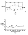
- FIG. 7 is a timing diagram illustrating the operation of the sample rate converter according to the preferred embodiment of the invention.
- FIG. 8 is a plot of AM signal strength illustrating the effect of the AM interference accomplished according to the preferred embodiment of the invention.
- the present invention will be described in connection with its preferred embodiment, namely as implemented into a digital audio receiver, specifically a digital audio receiver that receives amplitude modulated (AM) input signals such as provided by way of conventional AM radio audio signals and as conventional television signals.
- AM amplitude modulated
- This description is provided because this invention is particularly beneficial when used in such a context.
- this invention may be used to advantage in other audio and signal processing applications. Accordingly, it is to be understood that the following description is provided by way of example only, and is not intended to limit the true scope of this invention as claimed.
- FIG. 1 a illustrates, in block diagram form, an audio system including digital audio receiver 2 , constructed according to the preferred embodiment of the invention.
- receiver 2 receives audio signals from multiple sources, including radio broadcasts via AM/FM tuner 6 , DVD loader 7 and MPEG decoder 9 .
- AM radio signals received by tuner 6 and audio DVD tracks from DVD loader 7 are in the form of amplitude modulation (AM) signals.
- AM amplitude modulation
- AM/FM tuner 6 includes conventional tuner circuitry, coupled to antenna A, for receiving and demodulating broadcast radio signals at the desired carrier frequency.
- front panel controls 12 are provided, by way of which the user can select the desired radio station.
- the desired station frequency is read from front panel controls 12 by system microcontroller 14 , which in turn communicates the desired frequency to AM/FM tuner 6 .
- Conventional circuitry is provided within tuner 6 for recovering the signal at the desired frequency. For example, as shown in FIG.
- tuner 6 may be a conventional superheterodyne tuner circuit, including RF amplifier 11 a , which amplifies the received signal at the desired AM tuned frequency f c , which is the carrier frequency of the desired amplitude-modulates signal.
- the AM tuned frequency f c is selected by the listener via front panel controls 12 , is communicated to system microcontroller 14 .
- tuning circuitry 11 f in tuner 6 controls amplifier 11 a accordingly, and also controls the application of a periodic signal by local oscillator 11 c to mixer 11 b .
- the amplified modulated signal at the AM tuned frequency f c is also applied to mixer 11 b , for downconverting of the modulated signal at AM tuned frequency f c to a desired intermediate frequency IF.
- intermediate frequency IF is a fixed frequency, such as 455 kHz for most AM radios or 262.5 kHz for automobile radios, regardless of the AM tuned frequency f c .
- Tuning circuitry 11 f thus controls local oscillator 11 c to output a signal at a frequency that differs from carrier frequency f c by the intermediate frequency IF.
- the downconverted signal at intermediate frequency IF is then amplified by IF amplifier 11 d , and demodulated to baseband by analog demodulator 11 e .
- the resulting baseband signal from demodulator 11 e is then converted to a digital datastream by analog-to-digital converter (ADC) 13 at a selected sampling frequency f s , typical values of which are 44.1 kHz and 48 kHz.
- ADC
- AM tuner architectures are known in the art, including both analog tuners of types other than the superheterodyne tuner shown in FIG. 1 b , and also including digital tuners. These other architectures can alternatively be implemented into digital audio system 2 of FIG. 1 a , according to the preferred embodiment of the invention.
- digital audio amplifier 8 includes digital audio pulse-width-modulation (PWM) processor 10 , the construction of which will be described in further detail below.
- PWM processor 10 generates pulse-width-modulated (PWM) pulse trains that are used by drive circuitry (within digital audio amplifier 10 , but not shown) to drive an output device, such as speaker SPKR, in class D fashion.
- drive circuitry within digital audio amplifier 10 , but not shown
- PWM processor 10 will have the capability of driving multiple audio channels, and thus multiple speakers SPKR as is well known in the art. In such multiple channel cases, tuner 6 will be providing multiple datastreams, each corresponding to one of these channels.
- PCM pulse-code-modulated
- PWM pulse-code-modulated
- a high-speed clock is involved in the generation of the output PWM signal, with the resolution of the PWM signal corresponding to the relationship of the high-speed clock to the PWM frame rate.
- a typical high-speed PWM clock frequency is a multiple of 512 times that of the PWM frame rate (providing eight bits of resolution in the PCM-to-PWM conversion).
- typical PWM frame rates can cause interference with the AM signal being demodulated and processed.
- a PWM typical frame rate in digital audio of 384 kHz has a second harmonic of 768 kHz; this second harmonic is within the standard AM frequency band, and will interfere with the receipt of radio signals at and near 768 kHz.
- a common intermediate frequency in AM demodulation is 455 kHz; a PWM frame rate at or near 455 kHz will interfere with the intermediate demodulated signal at that IF.
- the present invention is intended to reduce interference caused by the PWM frame rate clock signal.
- DVD loader 7 and MPEG decoder 9 can operate in combination to provide digital audio signals from a DVD movie or the like; such digital audio streams are typically at a sampling frequency f s of 32 kHz in modern systems. Upconverting of this sampling frequency f s is also accomplished by PWM processor 10 according to this embodiment of the invention, as will be described in further detail below.
- FIG. 2 illustrates, in further detail, the construction of PWM processor 10 according to the preferred embodiments of the invention.
- PWM processor 10 drives four output audio channels from four separate digital inputs from tuner 6 or elsewhere. It is, of course, contemplated that digital audio system 2 may drive more or fewer channels, depending upon the system requirements and specifications.
- PWM processor 10 is preferably implemented as a single integrated circuit for performing much of the digital domain audio processing for the multiple audio channels. Processor 10 may, alternatively, be implemented by multiple integrated circuits, if appropriate for a particular application.
- digital audio processing function 15 has multiple inputs that are coupled to one or more audio sources, and that receives four input signals DIN_ 1 through DIN_ 4 , in the form of digital datastreams at sampling frequency f s .
- Digital audio processing function 15 includes conventional circuitry for performing the conventional functions of parametric speaker equalization or “voicing”, implementation of graphic equalizer presets, treble and bass adjustment, precision soft volume control on the audio signal being processed for its channel.
- Other digital functions that can be performed by digital audio processing function 15 include loudness compensation to boost the bass frequencies when the output for the channel is low, dynamic range compression, background noise floor compensation or noise squelch, center or sub-woofer channel synthesis, programmable dither, peak limiting and clipping, and other digital filter processing. These functions are typically performed by the application of biquad, or second-order IIR, digital filters in a cascade arrangement.
- Audio amplifier channels 20 1 through 20 4 drive class D pulse-width-modulated (PWM) output signals PWM_ 1 through PWM_ 4 , respectively, according to the processed digital audio input signals for their respective channels, as processed by digital audio processor 16 .
- PWM output signals PWM_ 1 through PWM_ 4 are applied to power stage circuits 22 1 through 22 4 , respectively, located elsewhere within digital audio amplifier 8 ( FIG. 1 a ).
- Power stage circuits 22 1 through 22 4 in turn drive respective ones of speakers SPKR_ 1 through SPKR_ 4 , either in a single-ended or a differential mode, by way of output signals PWM_ 1 through PWM_ 4 .
- Controller 13 provides the conventional control functions for processor 10 , such functions, including overvoltage and undervoltage detection and protection, detection and control related to other faults in the operation of processor 10 , the receipt and processing of mute signal MUTE, the receipt of user-programmable values for configuring and controlling processor 10 , and, according to this invention, clock circuitry for generating the various clock signals used by processor 10 .
- digital audio processor 15 is controlled by clock and control signals from controller 13 , and from other control functions within processor 10 (not shown).
- digital audio processing function 15 applies the appropriate signal processing to the digital audio signal according to the functions of digital audio system 2 .
- the output signal from digital audio processing function 15 is a pulse-code-modulated (PCM) signal, in which each sample of the data stream is expressed in a multiple-bit (e.g., 24-bit) data word of a value corresponding to the instantaneous amplitude of the signal at that sample time.
- PCM pulse-code-modulated
- Digital audio processing function 15 is clocked by a clock signal at sampling frequency f s , as generated by sample clock circuitry 25 in controller 13 .
- the PCM input signal is converted to a pulse-width-modulated (PWM) signal to drive speaker SPKR for the corresponding channel 20 k .
- PWM pulse-width-modulated
- interpolation function 16 receives the PCM signal that is at sampling frequency f s , and oversamples the processed PCM input signal to a sample rate that is a multiple N of this sampling frequency f s .
- a sampling clock signal at frequency Nf s is generated by sample clock circuitry 25 , and clocks the datastream into interpolation filter 16 .
- the multiple N may remain fixed (e.g., at a multiple of eight); alternatively, according to other embodiments of the invention, this multiple N may be adjusted to provide additional degrees of freedom in selection of a PWM frame rate that minimizes electromagnetic interference and other noise effects, as will be described below.
- the oversampling applied by interpolation filter 16 may be effected by repeating each input value by the oversampling multiple N, at the higher frequency Nf s .
- the output of interpolation filter 16 is thus an oversampled datastream, at a frequency corresponding to the multiple N times the input sampling frequency f s .
- sample rate converter 17 converts the sample rate of the interpolated signal at its input to a sample rate, corresponding to the eventual PWM frame rate, that generates reduced electromagnetic interference at the tuned AM frequency and any intermediate demodulation frequencies.
- the selection of a sample rate conversion ratio M depends on the AM tuned frequency f c , intermediate frequency IF, the desired PWM clock rate, and the bandwidth of the output audio signal, as will be described in further detail below.
- sample rate converter 17 receives the interpolated datastream at sampling frequency multiple Nf s , and generates a datastream at the desired converted sampling frequency f sc , based on a clock signal that is generated by sample clock circuitry 25 and sample rate control logic 27 in controller 13 , with the selection of the desired converted sampling frequency f sc (and, optionally, the multiple N) made by sample rate control logic 27 in response to control signals from system microcontroller 14 ( FIG. 1 a ).
- the selection of the desired converted sampling frequency f sc and its implementation by way of controller 13 will be described below.
- sample rate converter 17 amounts to a zero-order hold of the incoming datastream from interpolation filter 16 , followed by a resampling at converted sampling frequency f sc . It has been discovered, according to this invention, that this resampling can be effected without requiring additional filtering to eliminate spurious noise from the audible band, by properly selecting the sample rate conversion ratio and thus the PWM frame rate.
- PWM 23 in this embodiment of the invention, includes multiple functions. As shown in the generalized illustration of FIG. 3 , PWM 23 includes filtering sequence 19 , which includes such conventional functions as noise shaping, digital non-linear correction, click and pop reduction, inter-channel delay processing, and the like. Examples of preferred implementations of filtering sequence 19 are described in copending applications Ser. No. 10/962,848 and Ser. No. 10/963,239, both filed Oct. 12, 2004, and copending application Ser. No. 10/988,268, filed Nov. 12, 2004, all commonly assigned herewith and incorporated herein by this reference.
- PCM to PWM conversion function 21 then generates output pulse trains as PWM signals corresponding to the PCM output of filtering sequence 19 .
- PCM to PWM conversion function 21 is preferably implemented by digital circuitry that digitally calculates the times at which rising and falling edges of the PWM output signals are to be issued. In this manner, the reference triangle waveform may simply be a high-speed clock signal.
- the digital circuitry can simply receive the input PCM signal on line PCM_in, and digitally calculate the edges of the differential PWM pulses, including the desired filtering.
- Conventional high-speed digital signal processing circuitry is capable of carrying out these calculations sufficiently rapidly for driving digital audio output PWM signals, as known in the art.
- PCM to PWM conversion function 21 suitable for use in connection with the preferred embodiments of this invention are also described in the above-incorporated applications Ser. No. 10/962,848, Ser. No. 10/963,239, and Ser. No. 10/988,268.
- Filtering sequence 19 operates according to the converted sampling frequency f sc , while PCM to PWM conversion function 21 receives high-speed clock DCLK from sample clock circuitry 25 , by way of which the duty cycle of the output PWM signal is adjusted according to the amplitude of the PCM input signal.
- High-speed clock DCLK is typically at a much higher frequency than the sampling frequencies f sc ; for example at a multiple of 512 to provide nine bits of resolution.
- the resulting PWM pulses, at a PWM frame rate equal to the converted sampling frequency f sc are then forwarded on to the corresponding drive stage 22 k ( FIG. 2 ) for channel 20 k .
- sample clock circuitry 13 provides a clock signal at sampling frequency f s to digital audio processor 15 , and a clock signal at sampling frequency multiple Nf s to interpolation filter 16 .
- sample clock circuitry 13 provides high speed clock DCLK to PCM to PWM conversion function 21 , and a clock signal at the desired converted sampling frequency f sc to sample rate converter 17 and to PCM to PWM conversion function 21 .
- sample clock circuitry 13 includes digital phase-locked loop (DPLL) 34 , which receives a reference clock signal, for example at sampling frequency f s , and which in turn generates a clock signal at sampling clock multiple frequency Nf s accordingly.
- the clock signal at sampling clock multiple frequency Nf s is applied to frequency divider 32 , which in turn generates the sampling clock at sampling frequency f s , and applies that sampling clock to digital audio processor 15 .
- the clock signal at sampling clock multiple frequency Nf s is applied to interpolation filter 16 .
- the PCM signal on line DIN is input to digital audio processor 15 , and processed according to the desired approach, in a synchronous manner at sampling frequency f s , as described above.
- the output processed datastream from digital audio processor 15 which is also at sampling frequency f s is applied to interpolation filter 16 , which oversamples this datastream at the multiple N to generate an oversampled datastream at sampling clock multiple frequency Nf s that is applied to sample rate converter 17 , and there converted to converted sample frequency f sc .
- Sample clock circuitry 13 also includes analog PLL 36 , which is a conventional analog phase-locked loop that generates high speed clock DCLK from the reference clock signal (e.g., at sampling frequency f s ), and in response to a sample rate conversion ratio M provided by sample rate control logic 27 .
- APLL 36 generates high speed clock DCLK and applies it to PCM to PWM conversion function 21 , and to frequency divider 38 .
- analog PLLs such as APLL 36 are readily controllable to generate clock signals at desired multiples, by controlling input and feedback frequency dividers within the PLL.
- ratio M from sample rate control logic 27 is preferably applied to either an input or feedback frequency divider in APLL 36 , to control the frequency of the output signal from APLL 36 in the conventional manner.
- Frequency divider 38 divides down the frequency of high speed clock DCLK, preferably by a fixed value (e.g., 512), and generates clock signals at converted sample rate frequency f sc that are applied to sample rate converter 17 and to PCM to PWM conversion function 21 .
- Sample rate converter 17 converts the data stream from interpolation filter 16 , at sampling clock multiple frequency Nf s , to a datastream at converted sample rate frequency f sc .
- Converted sample rate frequency f sc also serves as the PWM frame rate, in this embodiment of the invention, according to which PCM to PWM conversion function 21 converts the PCM datastream from sample rate converter 17 to the appropriate PWM control signals, as described above.
- FIG. 5 a illustrates the construction of sample rate converter 17 according to the preferred embodiment of the invention. It has been discovered, according to this invention, that proper selection of the particular ratio M enables this simple construction, without requiring digital filtering or other complex processing in order to avoid audible noise. The selection of ratio M in this regard will be described in further detail below.
- sample rate converter 17 includes a first sample and hold circuit 40 a , which is clocked at sampling rate multiple frequency Nf s , and is simply a zero-order hold circuit. The output of sample and hold circuit 40 a is then again merely resampled, by sample and hold circuit 40 b , but at a clock rate corresponding to converted sample rate frequency f sc .
- the converted sampling rate frequency f SC which equals (and will be, for purposes of this description, synonymous with) the PWM frame rate, is selected according to the AM tuned frequency f c .
- the selection of the PWM frame rate is effected by selecting an appropriate sample rate conversion ratio M to be applied by sample rate converter 17 , with the selection of ratio M being made in response to the AM tuned frequency f c .
- An additional degree of freedom in the adjustment of the PWM frame rate can be obtained by also adjusting the value of multiple N, although it is contemplated that a fixed oversampling multiple N will generally be sufficient.
- the PWM frame rate can cause interference with AM demodulation and reception if it and its lower harmonics are near the AM tuned frequency f c itself, near the intermediate frequency IF, or near an image of the intermediate frequency IF (i.e., the tuned frequency plus twice the IF).
- a set of PWM frame rate frequencies f sc and corresponding DCLK rates f DCLK are:
- the particular sample rate conversion ratio M is selected from among a set of candidate values, according to particular tests that will now be described relative to FIG. 6 .
- the process of FIG. 6 associates a sample rate conversion ratio M with each discrete AM tuned frequency f c . Accordingly, the process of FIG. 6 may be performed in real time upon the selection of an AM tuned frequency f c during the operation of the audio system. Alternatively, and indeed preferably, the process of FIG. 6 is performed prior to the manufacture and use of digital audio system 2 to associate each possible AM tuned frequency f c with a sample rate conversion ratio M and to store those associations in memory; in this case, sample rate control logic 27 can operate in response to a given AM tuned frequency f c by retrieving the appropriate ratio M and applying that ratio to sample clock circuitry 25 .
- one or more “profiles” may be stored in memory, for example in controller 13 (e.g., SRC ratio memory 29 of FIG. 3 ) or in system microcontroller 14 , each profile including a set of associations of sample rate conversion ratio values M for each of the possible AM tuned frequencies.
- the user or system manufacturer can then select from among the profiles, depending upon the performance desired.
- digital audio system 2 can operate according to various sampling frequencies f s (e.g., 32 kHz, 44.1 kHz, and 48 kHz)
- multiple profiles may also be characterized and stored to accommodate the different sampling frequencies.
- the process of FIG. 6 in which the PWM frame rate and associated frequencies are selected and associated with specific AM tuned frequencies, may be performed by system microcontroller 14 within the digital audio system; alternatively, if the selection and association of PWM frame rate is being performed prior to manufacture of digital audio system 2 , such as in a characterization operation, this process may be executed by a conventional computer workstation or the like.
- this association process begins with process 50 , in which a specific AM tuned frequency f c is selected.
- a set of several discrete sample rate conversion ratios are preferably defined in advance.
- An example of such a set of ratios are those illustrated in the above table (e.g., 5/8, 6/8, . . . , 12/8).
- a first one of these ratios is selected as a candidate sample rate conversion ratio.
- this frequency can be tested to determine whether it would cause undesirable interference with the AM signal, both as received and as demodulated.
- this testing of the PWM frame rate f sc involves three separate tests: (i) whether the PWM frame rate or its first k harmonics (where k is typically 5 or 6) interfere with the AM tuned frequency f c ; (ii) whether the fundamental PWM frame rate or any of its lower harmonics interfere with the intermediate frequency IF generated in AM demodulation; and (iii) whether the fundamental PWM frame rate or its lower harmonics interfere with an image frequency corresponding to the difference between the AM tuned frequency f c and the second harmonic of the IF.
- other interference tests may also be performed, as appropriate for the particular digital audio system; conversely, one or more of these tests may be omitted if unnecessary to ensure the required fidelity for the particular system.
- decision 55 a determines whether the calculated PWM frame rate f sc would cause interference with the AM tuned frequency selected in process 50 .
- decision 55 a is performed by comparing the calculated PWM frame rate f sc , and also its second harmonic (2f sc ) with the AM tuned frequency. If the calculated PWM frame rate f sc , and its second harmonic, differ from the AM tuned frequency f c by greater than an “interference bandwidth” value, this test criterion is met.
- the interference bandwidth is a frequency difference that has been observed, or is believed, to be a sufficient difference so that interference does not result.
- different harmonics of the PWM frame rate f sc may have different interference bandwidth values associated therewith, because of the spreading of energy at those harmonics, and also because the AM tuner is sensitive in a bandwidth around the center, AM tuned, frequency.
- An example of a set of interference bandwidths, varying with the harmonics of the PWM frame rate, is:
- decision 55 a will determine whether both the calculated PWM frame rate f sc , and the calculated frame rate second harmonic 2f sc , differ from the AM tuned frequency f c by more than 17.5 kHz. If not (for either the fundamental or the 2 nd harmonic), decision 55 a returns a NO result, and control passes to decision 57 , as will be described below.
- Decision 55 b determines whether any of the calculated PWM frame rate fundamental frequency f sc and its lower harmonics will interfere with the intermediate frequency IF in tuner 6 ( FIG. 1 b ). Again, the interference bandwidth values determine whether such interference will be caused by these calculated frame rate harmonics. According to an exemplary implementation of the preferred embodiment of the invention, the fundamental of the calculated PWM frame rate f sc and its second through sixth harmonics are compared against the intermediate frequency IF to determine whether any of these frequencies are within the interference bandwidth of intermediate frequency IF. If any of these harmonics is within its interference bandwidth, decision 55 b returns a NO result and control passes to decision 57 . If none of these harmonics are within their interference bandwidth of intermediate frequency IF, decision 55 b returns a YES result and the next test is evaluated, as shown by decision 55 c of FIG. 6 .
- Decision 55 c determines whether any of the calculated PWM frame rate fundamental frequency f sc and certain of its lower harmonics will interfere with an image frequency that is generated in tuner 6 .
- This image frequency ImF is the difference between the second harmonic of the AM tuned frequency f c and the intermediate frequency IF; interference at this image frequency ImF has been observed to reduce the sensitivity of the AM tuner, as known in the art.
- the fundamental and second through sixth harmonics of PWM frame rate f sc are analyzed to determine whether any are within the interference bandwidth of this image frequency ImF. If so, decision 55 c returns a NO result and control passes to decision 57 .
- a NO result from any of decisions 55 indicates that the currently selected candidate sample rate conversion ratio M cannot be used, because of the interference that the corresponding PWM frame rate f sc would cause at tuner 6 .
- Decision 57 determines whether more candidate ratios M are yet to be analyzed for interference; if so (decision 57 is YES), the next candidate ratio M is selected in process 58 , and the new PWM frame rate f sc is calculated in process 54 and tested in decisions 55 . If all of the candidate ratios M have been analyzed (decision 57 is NO), then no sample rate conversion ratio M is available that does not cause AM tuning interference.
- FIG. 7 illustrates the cause of this possible audible noise at sample rate converter 17 , for a simplified case in which interpolation filter 16 generates four interpolated samples of the input amplitude, and in which sample rate converter 17 re-samples this sample stream at a frequency f sc that is five times the input sample frequency (and therefore 5/4 times the frequency of the output of interpolation filter 16 ).
- f sc the frequency of the interpolation filter 16 output
- FIG. 7 illustrates sample points S indicating the resampling by sample rate converter at the higher frequency.
- sample and hold circuit 40 b samples one of the interpolated amplitude values twice, in each periodic pattern. This re-sampling is reflected, in a frequency domain representation of the output of sample rate converter 17 , by a spike at a frequency related to the difference between the two frequencies at the input and output of sample rate converter 17 .
- process 60 the calculated PWM frame rate f sc is compared against the sampling frequency f s to determine a difference frequency and its harmonics.
- decision 61 these difference frequencies (fundamental and harmonics) are compared against the upper frequency of the audio bandwidth desired from digital audio system 2 .
- process 60 and decision 61 evaluate:
- all of the candidate ratios M may be processed through process 54 and decisions 55 , and those that do not cause AM interference can all be identified before the selection from among these possible ratios M is made.
- a NO result from decision 61 would result in selection of the next candidate ratio M that passed decisions 55 a through 55 c in this example.
- the currently selected sample rate conversion ratio M is suitable for use at the current AM tuned frequency.
- This ratio M is then preferably stored in memory in association with the current AM tuned frequency; for example, this value of ratio M may be stored in SRC ratio memory 29 of controller 13 , as shown in FIG. 3 , either if calculated during system operation or calculated prior to manufacture.
- the process of FIG. 6 may then be repeated, either for all possible AM tuned frequencies tunable by tuner 6 if performed before manufacture, or for each new AM tuned frequency encountered during operation if these calculations are performed on-board, during system operation.
- the set of sample rate conversion ratios M are restricted so that the tones that cause audible noise are avoided.
- the upsampling ratio N*M i.e., the product of the oversampling multiple N and the sample rate conversion ratio M
- the resulting aliasing tones generated in the resampling by sample rate converter 17 will be above the Nyquist frequency of the input signal.
- the application of this integer upsampling ratio N*M shifts the tone frequency by that integer value times the input sampling rate f s away from the baseband frequency.
- multiple sets of associated sample rate conversion ratios M may be provided within digital audio system 2 , for example as stored in SRC ratio memory 29 as shown in FIG. 3 .
- the particular set of associated ratios M that are to be enabled and used may be selected in the manufacture of digital audio system 2 , for example by hardwiring certain otherwise unused external terminals of digital audio processor 10 into a pattern, or under software control (e.g., calling a particular sequence by way of a digital word written into a control register or the like).
- Digital audio system 2 is then ready for use, including as an AM radio receiver.
- system microcontroller 14 interprets the desired carrier frequency f c for that AM station, and communicates, by way of digital control signals, the AM tuned frequency f c to tuner 6 and to PWM processor 10 in digital audio amplifier 8 . As shown in FIG. 2 , these digital control signals AM_TF are applied to controller 13 of PWM processor 10 . In response to the selected AM tuned frequency, referring to FIG.
- sample rate control logic 27 determines the associated sample rate conversion ratio M for that AM tuned frequency f c , for example by interrogating SRC ratio memory 29 for a selected sequence of ratio values, and controls sample clock circuitry 25 to generate the appropriate clock signals including high-speed clock DCLK and the clock signals applied to sample rate converter 17 at the converted sampling rate (PWM frame rate) frequency f SC .
- FIG. 5 b illustrates the construction of APLL 36 in sample clock circuitry 13 , by way of which the appropriate high speed clock DCLK, and precursor for the divided-down converted sampling rate (PWM frame rate) frequency f SC , are generated according to the preferred embodiment of the invention.
- APLL 36 includes prescale frequency divider 70 , which receives the reference signal at sampling frequency f s in this example, and generates a divided-down clock signal at frequency f s /k, where the integer k is the divisor of prescale frequency divider 70 , generated by frequency scale logic 77 in response to the current value of sample rate conversion ratio M.
- phase detector 72 This clock is applied to one input of phase detector 72 , the other input of which receives a feedback signal from frequency divider 78 .
- the output of phase detector 72 drives, via loop filter 74 , voltage controlled oscillator 76 .
- VCO 76 generates high-speed clock signal DCLK, which is also fed back to frequency divider 78 .
- Frequency divider 78 divides down the frequency of clock signal DCLK by a factor of 512 times integer j; integer j is generated by frequency scale logic 77 in response to the current value of sample rate conversion ratio M.
- the frequency of high speed clock DCLK is 512 times the sampling frequency f s , times the ratio j/k.
- the input reference clock to APLL 36 may be at a higher frequency, for example a reference frequency selected from a list of multiples of sampling frequency f s (e.g., 256f s , 512f s , 384f s , etc.), which will permit frequency divider 78 to divide down its input by a factor of j.
- f s multiples of sampling frequency
- Other combinations will be similarly derivable by those skilled in the art having reference to this specification.
- frequency scale logic 77 generates the integers j, k in response to the sample rate conversion ratio M communicated from controller 13 .
- These integers j, k set the high speed clock DCLK frequency, and via frequency divider 38 ( FIG. 4 ), the PWM frame rate frequency f sc .
- plots of AM tuner sensitivity performance illustrate an example of improved AM tuner performance provided by the preferred embodiment of the invention.
- Plot 70 illustrates the AM signal strength as a function of AM tuned frequency f c , in which sample rate converter 17 is operated according to the preferred embodiment of the invention, using an example of an sequence of sample rate conversion ratios M generated according to the process of FIG. 6 .
- Plot 72 illustrates the AM signal strength with no sample rate conversion applied.
- this embodiment of the invention is able to greatly improve the AM signal strength around the AM tuned frequencies f c between about 750 kHz and 925 kHz, and also at frequencies above about 1450 kHz; in this example, the uncorrected PWM frame rate (i.e., a PWM frame rate of Nf s ) causes significant interference at these frequencies. According to the preferred embodiment of the invention, therefore, substantial improvement in the AM sensitivity and fidelity is provided, in a very efficient manner.
- selection of the appropriate sample rate conversion ratio M to avoid AM interference, and to also avoid audible noise from sample rate converter 17 itself, is effected simply by changing the prescale and feedback divider integers j, k; these multipliers are preferably precalculated, so that they can be generated by simple logic as described above relative to FIG. 6 .
- This invention may also be used to account for changes in the sampling frequency f s , such as can occur when a different audio source is utilized.
- DVD audio may be provided at a lower sampling rate f s , for example 32 kHz. While no AM tuning is performed to amplify this audio signal, and thus AM interference from the PWM frame rate is not an issue, the use of this lower sampling rate f s may cause some functions, such as noise shaping filter function 19 ( FIG. 3 ) to operate at too low a frequency, resulting in noise in the upper portion of the audio band.
- sample rate converter 17 can be controlled, responsive to the selection of the audio source (or in response to the digital audio sampling rate f s ), to re-sample the output of interpolation filter 16 to increase the PWM frame rate at PWM conversion function 21 .
- system microcontroller 14 would receive user inputs, from front panel controls 12 , indicating that DVD loader 7 is the source of audio signals. These audio signals are applied to MPEG decoder 9 .
- System microcontroller 14 enables MPEG decoder 9 to generate digital audio signals on lines DIG_AUD, at a sampling rate f s of 32 kHz, in response to the audio signals retrieved by DVD loader.
- PWM processor 10 receives these digital audio signals, similarly as in the case of audio signals from tuner 6 described above.
- system microcontroller 14 also indicates, to PWM processor 10 , that the sampling rate f s of the digital audio from MPEG decoder 9 is at the lower rate, e.g., 32 kHz, and that sample rate converter 17 is to apply a sample rate conversion ratio M that upsamples the interpolated datastream by a precalculated multiple.
- This ratio M can be selected, in a manner similar as processes 60 through 62 ( FIG. 6 ) to ensure that sample rate converter 17 itself does not generate audible noise; as a result, no additional filtering or other complex processing is required to effect the sample rate conversion according to this embodiment of the invention.
- This would result in a high-speed clock signal DCLK at a frequency of about 197 MHz, and a converted sampling frequency (and PWM frame rate) f sc of 384 kHz.
- the PWM frame rate in a digital audio system can be easily adjusted, for example in response to the AM tuned frequency of an AM tuner in the system, or in response to a change in the digital input audio sampling rate.
- This adjustment in the PWM frame rate results in improved audio output fidelity, for example by avoiding the generation of AM interference, or by ensuring adequate sample rates so that digital audio processing does not itself generate audible noise.
- the adjustment of the sample rate conversion is effected by relatively simple logic, for example which controls an analog PLL, in response to a preselected pattern of sample rate conversion ratios that are calculated for various AM tuned frequencies, or for expected input audio sampling frequencies.
- the determination and implementation of the sample rate conversion is therefore extremely efficient, and can be carried out in effectively a transparent manner insofar as the system user is concerned, and can be implemented at very low cost.
Landscapes
- Engineering & Computer Science (AREA)
- Power Engineering (AREA)
- Noise Elimination (AREA)
Abstract
Description
f DCLK =R*f sc =R*(M*N*f s)
where R is the multiple of the high-speed clock signal relative to the converted sample rate frequency fsc. For example, as noted above, resolution multiple R is preferably fixed to a relatively high multiple, such as R=512, to provide good resolution in the audio output.
| M = 5/8 | M = 6/8 | M = 7/8 | M = 8/8 | M = 9/8 | M = 12/8 | ||
| | 221 kHz | 265 kHz | 309 kHz | 353 kHz | 397 kHz | 529 kHz |
| ƒDCLK | 113 MHz | 136 MHz | 158 MHz | 181 | 203 MHz | 271 MHz |
According to the preferred embodiment of the invention, the particular sample rate conversion ratio M is selected from among a set of candidate values, according to particular tests that will now be described relative to
f sc =M*N*f s
| Harmonic of PWM frame rate ƒsc | Interference bandwidth (kHz) |
| Fundamental | 17.5 |
| 2nd harmonic | 17.5 |
| 3rd harmonic | 17.5 |
| 4th harmonic | 20.0 |
| 5th harmonic | 22.5 |
| 6th harmonic | 23.5 |
According to this example, therefore,
for reasonable integer values of n and k. If any component of this calculated frequency f for the currently selected sample rate conversion ratio M is within the audio band (i.e., less than faudio), then an audible component of spurious noise would be caused by
| M = 5/8 | M = 6/8 | M = 7/8 | M = 8/8 | M = 9/8 | M = 12/8 | ||
| | 60 | 72 | 56 | 64 | 72 | 72 |
| | 12 | 12 | 8 | 8 | 8 | 6 |
| ƒDCLK | 113 MHz | 136 MHz | 158 MHz | 181 | 203 MHz | 271 MHz |
| ƒSC | 221 kHz | 265 kHz | 309 kHz | 353 kHz | 397 kHz | 529 kHz |
These frequencies, in addition to being generated in a simple and elegant manner, are selectable as described above relative to
Claims (19)
Priority Applications (1)
| Application Number | Priority Date | Filing Date | Title |
|---|---|---|---|
| US11/118,831 US7809346B2 (en) | 2005-04-29 | 2005-04-29 | Digital audio receiver with reduced AM interference |
Applications Claiming Priority (1)
| Application Number | Priority Date | Filing Date | Title |
|---|---|---|---|
| US11/118,831 US7809346B2 (en) | 2005-04-29 | 2005-04-29 | Digital audio receiver with reduced AM interference |
Publications (2)
| Publication Number | Publication Date |
|---|---|
| US20060247810A1 US20060247810A1 (en) | 2006-11-02 |
| US7809346B2 true US7809346B2 (en) | 2010-10-05 |
Family
ID=37235517
Family Applications (1)
| Application Number | Title | Priority Date | Filing Date |
|---|---|---|---|
| US11/118,831 Active 2029-06-25 US7809346B2 (en) | 2005-04-29 | 2005-04-29 | Digital audio receiver with reduced AM interference |
Country Status (1)
| Country | Link |
|---|---|
| US (1) | US7809346B2 (en) |
Cited By (8)
| Publication number | Priority date | Publication date | Assignee | Title |
|---|---|---|---|---|
| US20090238382A1 (en) * | 2008-03-19 | 2009-09-24 | Sanyo Electric Co., Ltd. | Audio reproduction system |
| US20100182062A1 (en) * | 2009-01-21 | 2010-07-22 | Gautham Devendra Kamath | Audio processor with internal oscillator-generated audio intermediate frequency reference |
| US20120166139A1 (en) * | 2009-06-24 | 2012-06-28 | Christian Schmidmer | Device and Method for Determining a Sample Rate Difference |
| US8648738B1 (en) * | 2012-06-15 | 2014-02-11 | Altera Corporation | Apparatus and methods of rate control for a sample rate converter |
| US20140128004A1 (en) * | 2012-11-08 | 2014-05-08 | Stmicroelectronics Asia Pacific Pte Ltd. | Converting samples of a signal at a sample rate into samples of another signal at another sample rate |
| US8842787B1 (en) * | 2006-03-08 | 2014-09-23 | Marvell International Ltd. | Receiver employing selectable A/D sample clock frequency |
| US10593337B2 (en) * | 2015-07-10 | 2020-03-17 | Sony Corporation | Transmission apparatus, transmission method, reception apparatus, and reception method |
| US10700696B1 (en) | 2019-04-18 | 2020-06-30 | Raytheon Company | Adaptive control circuit and method for signal-optimized sampling |
Families Citing this family (12)
| Publication number | Priority date | Publication date | Assignee | Title |
|---|---|---|---|---|
| US8559570B2 (en) * | 2005-06-30 | 2013-10-15 | Silicon Laboratories Inc. | Cancellation of undesired portions of audio signals |
| US20090135897A1 (en) * | 2006-10-04 | 2009-05-28 | Yasuhito Soma | Semiconductor integrated circuit and electronic device |
| US7391346B1 (en) * | 2007-02-05 | 2008-06-24 | Sigmatel, Inc. | Switching amplifier system and method |
| US20080310336A1 (en) * | 2007-06-15 | 2008-12-18 | Broadcom Corporation | Dynamic receiver filter adjustment across preamble and information payload |
| JP5212208B2 (en) * | 2009-03-23 | 2013-06-19 | 沖電気工業株式会社 | Receiving apparatus, method and program |
| JP5444863B2 (en) * | 2009-06-11 | 2014-03-19 | ソニー株式会社 | Communication device |
| US20110074211A1 (en) * | 2009-09-25 | 2011-03-31 | Lear Corporation | Apparatus and method for controlling the switching frequency of a power converter |
| TWI505661B (en) * | 2013-09-09 | 2015-10-21 | Elite Semiconductor Esmt | Amplitude modulation interference avoidance method, device, and amplitude modulation receiver |
| KR20150072987A (en) * | 2013-12-20 | 2015-06-30 | 삼성전자주식회사 | Noise Reduction Method and Electronic Device supporting the same |
| KR101567220B1 (en) * | 2014-06-05 | 2015-11-06 | 현대자동차주식회사 | Vehicle audio system and noise removal method of the same |
| TWI566241B (en) * | 2015-01-23 | 2017-01-11 | 宏碁股份有限公司 | Speech signal processing device and speech signal processing method |
| CN110086549B (en) * | 2019-04-02 | 2021-09-14 | 北京小米移动软件有限公司 | Audio data transmission method and device |
Citations (4)
| Publication number | Priority date | Publication date | Assignee | Title |
|---|---|---|---|---|
| US20020057115A1 (en) | 2000-09-29 | 2002-05-16 | Tsecouras Michael J. | Adaptive pulse frame rate frequency control for minimization of electro-magnetic contamination in integrated switching amplifier systems |
| US20030058973A1 (en) | 2001-06-01 | 2003-03-27 | Tsecouras Michael J. | Adaptive pulse frame rate frequency control for digital amplifier systems |
| US6748028B1 (en) | 1999-05-31 | 2004-06-08 | Stmicroelectronics S.R.L. | Digital AM demodulator, particularly for demodulating TV signals |
| US20050097154A1 (en) * | 2003-10-30 | 2005-05-05 | Tsecouras Michael J. | Noise reduction in systems with an RF tuner front end |
-
2005
- 2005-04-29 US US11/118,831 patent/US7809346B2/en active Active
Patent Citations (5)
| Publication number | Priority date | Publication date | Assignee | Title |
|---|---|---|---|---|
| US6748028B1 (en) | 1999-05-31 | 2004-06-08 | Stmicroelectronics S.R.L. | Digital AM demodulator, particularly for demodulating TV signals |
| US20020057115A1 (en) | 2000-09-29 | 2002-05-16 | Tsecouras Michael J. | Adaptive pulse frame rate frequency control for minimization of electro-magnetic contamination in integrated switching amplifier systems |
| US6456127B1 (en) | 2000-09-29 | 2002-09-24 | Texas Instruments Incorporated | Adaptive pulse frame rate frequency control for minimization of electro-magnetic contamination in integrated switching amplifier systems |
| US20030058973A1 (en) | 2001-06-01 | 2003-03-27 | Tsecouras Michael J. | Adaptive pulse frame rate frequency control for digital amplifier systems |
| US20050097154A1 (en) * | 2003-10-30 | 2005-05-05 | Tsecouras Michael J. | Noise reduction in systems with an RF tuner front end |
Cited By (12)
| Publication number | Priority date | Publication date | Assignee | Title |
|---|---|---|---|---|
| US8842787B1 (en) * | 2006-03-08 | 2014-09-23 | Marvell International Ltd. | Receiver employing selectable A/D sample clock frequency |
| US20090238382A1 (en) * | 2008-03-19 | 2009-09-24 | Sanyo Electric Co., Ltd. | Audio reproduction system |
| US20100182062A1 (en) * | 2009-01-21 | 2010-07-22 | Gautham Devendra Kamath | Audio processor with internal oscillator-generated audio intermediate frequency reference |
| US8452429B2 (en) * | 2009-01-21 | 2013-05-28 | Cirrus Logic, Inc. | Audio processor with internal oscillator-generated audio intermediate frequency reference |
| US20120166139A1 (en) * | 2009-06-24 | 2012-06-28 | Christian Schmidmer | Device and Method for Determining a Sample Rate Difference |
| US9037435B2 (en) * | 2009-06-24 | 2015-05-19 | Opticom Dipl.-Ing. Michael Keyhl Gmbh | Device and method for determining a sample rate difference |
| US8648738B1 (en) * | 2012-06-15 | 2014-02-11 | Altera Corporation | Apparatus and methods of rate control for a sample rate converter |
| US9112519B1 (en) * | 2012-06-15 | 2015-08-18 | Altera Corporation | Apparatus and methods of rate control for a sample rate converter |
| US20140128004A1 (en) * | 2012-11-08 | 2014-05-08 | Stmicroelectronics Asia Pacific Pte Ltd. | Converting samples of a signal at a sample rate into samples of another signal at another sample rate |
| US8874175B2 (en) * | 2012-11-08 | 2014-10-28 | Stmicroelectronics Asia Pacific Pte. Ltd. | Converting samples of a signal at a sample rate into samples of another signal at another sample rate |
| US10593337B2 (en) * | 2015-07-10 | 2020-03-17 | Sony Corporation | Transmission apparatus, transmission method, reception apparatus, and reception method |
| US10700696B1 (en) | 2019-04-18 | 2020-06-30 | Raytheon Company | Adaptive control circuit and method for signal-optimized sampling |
Also Published As
| Publication number | Publication date |
|---|---|
| US20060247810A1 (en) | 2006-11-02 |
Similar Documents
| Publication | Publication Date | Title |
|---|---|---|
| US7809346B2 (en) | Digital audio receiver with reduced AM interference | |
| US6717533B2 (en) | Method and apparatus for combining a wireless receiver and a non-wireless receiver | |
| US7003271B2 (en) | Direct conversion receiver having a gain-setting dependent filter parameter | |
| US20080214135A1 (en) | Methods and apparatus to perform noise cancellation in radios | |
| US20010048723A1 (en) | VSB/QAM receiver and method | |
| CN100438328C (en) | Demodulator circuit and corresponding method for simulating down-conversion | |
| US20090135897A1 (en) | Semiconductor integrated circuit and electronic device | |
| US8605222B2 (en) | Receiver device, tuner, and television receiver | |
| US6347123B1 (en) | Low-current sample rate converter | |
| JP2003198981A (en) | AGC control type intermediate frequency amplifier circuit | |
| US20110230153A1 (en) | Providing Channel Filtering In An Automatic Frequency Control Path | |
| US8842787B1 (en) | Receiver employing selectable A/D sample clock frequency | |
| US7248649B2 (en) | Digital baseband receiver including a time domain compensation module for suppressing group delay variation distortion incurred due to analog low pass filter deficiencies | |
| US7403066B2 (en) | Method and system for creating a spectral null in a switching amplifier | |
| CN100574093C (en) | Digital audio amplifier, system including same and method of amplifying audio signal | |
| US20030058973A1 (en) | Adaptive pulse frame rate frequency control for digital amplifier systems | |
| EP1396941B1 (en) | Time division IQ channel direct conversion receiver, and method therefor | |
| CN1871773B (en) | analog-to-digital conversion and suppression system | |
| US8036625B1 (en) | Method and apparatus for mixing a signal | |
| JP2020036277A (en) | Peak suppression circuit, peak suppression method, and transmission device | |
| JP2013012970A (en) | Semiconductor integrated circuit and operation method thereof | |
| JP2002009650A (en) | Fm receiver | |
| KR100964383B1 (en) | Digital Intensive RF Receiver | |
| WO2008142628A2 (en) | Receiver calibrating system and method | |
| JP2005064617A (en) | Multipath distortion elimination filter |
Legal Events
| Date | Code | Title | Description |
|---|---|---|---|
| AS | Assignment |
Owner name: TEXAS INSTRUMENTS INCORPORATED, TEXAS Free format text: ASSIGNMENT OF ASSIGNORS INTEREST;ASSIGNOR:OSSA, LUIS E.;REEL/FRAME:016526/0959 Effective date: 20050428 |
|
| AS | Assignment |
Owner name: TEXAS INSTRUMENTS INCORPORATED, TEXAS Free format text: ASSIGNMENT OF ASSIGNORS INTEREST;ASSIGNORS:RISBO, LARS;OSSA, LUIS E.;REEL/FRAME:016314/0557;SIGNING DATES FROM 20050428 TO 20050502 Owner name: TEXAS INSTRUMENTS INCORPORATED, TEXAS Free format text: ASSIGNMENT OF ASSIGNORS INTEREST;ASSIGNORS:RISBO, LARS;OSSA, LUIS E.;SIGNING DATES FROM 20050428 TO 20050502;REEL/FRAME:016314/0557 |
|
| STCF | Information on status: patent grant |
Free format text: PATENTED CASE |
|
| FPAY | Fee payment |
Year of fee payment: 4 |
|
| MAFP | Maintenance fee payment |
Free format text: PAYMENT OF MAINTENANCE FEE, 8TH YEAR, LARGE ENTITY (ORIGINAL EVENT CODE: M1552) Year of fee payment: 8 |
|
| MAFP | Maintenance fee payment |
Free format text: PAYMENT OF MAINTENANCE FEE, 12TH YEAR, LARGE ENTITY (ORIGINAL EVENT CODE: M1553); ENTITY STATUS OF PATENT OWNER: LARGE ENTITY Year of fee payment: 12 |