US7808357B2 - Dual inductance structure - Google Patents
Dual inductance structure Download PDFInfo
- Publication number
- US7808357B2 US7808357B2 US12/427,962 US42796209A US7808357B2 US 7808357 B2 US7808357 B2 US 7808357B2 US 42796209 A US42796209 A US 42796209A US 7808357 B2 US7808357 B2 US 7808357B2
- Authority
- US
- United States
- Prior art keywords
- conductor
- inductance
- grounding
- dual
- area
- Prior art date
- Legal status (The legal status is an assumption and is not a legal conclusion. Google has not performed a legal analysis and makes no representation as to the accuracy of the status listed.)
- Active
Links
- 230000009977 dual effect Effects 0.000 title abstract description 34
- 239000004020 conductor Substances 0.000 abstract description 159
- 239000000758 substrate Substances 0.000 abstract description 13
- 238000010586 diagram Methods 0.000 description 12
- 239000003990 capacitor Substances 0.000 description 7
- 230000000694 effects Effects 0.000 description 5
- 238000003780 insertion Methods 0.000 description 4
- 230000037431 insertion Effects 0.000 description 4
- 238000004891 communication Methods 0.000 description 3
- 238000000034 method Methods 0.000 description 2
- 238000012986 modification Methods 0.000 description 2
- 230000004048 modification Effects 0.000 description 2
- 238000013461 design Methods 0.000 description 1
- 238000012827 research and development Methods 0.000 description 1
- 238000004904 shortening Methods 0.000 description 1
- 238000007514 turning Methods 0.000 description 1
Images


Classifications
-
- H—ELECTRICITY
- H01—ELECTRIC ELEMENTS
- H01P—WAVEGUIDES; RESONATORS, LINES, OR OTHER DEVICES OF THE WAVEGUIDE TYPE
- H01P3/00—Waveguides; Transmission lines of the waveguide type
- H01P3/02—Waveguides; Transmission lines of the waveguide type with two longitudinal conductors
- H01P3/026—Coplanar striplines [CPS]
-
- H—ELECTRICITY
- H01—ELECTRIC ELEMENTS
- H01P—WAVEGUIDES; RESONATORS, LINES, OR OTHER DEVICES OF THE WAVEGUIDE TYPE
- H01P1/00—Auxiliary devices
- H01P1/20—Frequency-selective devices, e.g. filters
- H01P1/201—Filters for transverse electromagnetic waves
- H01P1/203—Strip line filters
- H01P1/20327—Electromagnetic interstage coupling
- H01P1/20354—Non-comb or non-interdigital filters
- H01P1/20381—Special shape resonators
Definitions
- the invention relates in general to an inductance structure, and more particularly to a dual inductance structure.
- FIG. 1A shows a conventional structural diagram of a miniaturized bandpass filter.
- FIG. 1B shows an equivalent circuit diagram of the miniaturized bandpass filter in FIG. 1A .
- the miniaturized bandpass filter 100 includes a conductor 102 , a conductor 104 , a conductor 106 , a conductor 108 and a conductor 110 , wherein the conductor 102 and conductor 104 are separated by a distance W 1 .
- the miniaturized bandpass filter 100 has an input port PORT 1 and an output port PORT 2 . Referring to both FIGS. 1A and 1B at the same time.
- the conductor 102 can be equivalent to an inductance L 1
- the conductor 104 can be equivalent to an inductance L 2
- the conductor 106 can be equivalent to a capacitor C 1
- the conductor 108 can be equivalent to a capacitor C 2
- the conductor 110 can be equivalent to a capacitor Cp.
- the input port PORT 1 corresponds to the input port P 1 of the equivalent circuit
- the output port PORT 2 corresponds to the output port P 2 of the equivalent circuit.
- the inductance L 1 and the inductance L 2 have the effect of mutual inductance.
- the distance W 1 As we may know that the smaller the distance W 1 is separated the larger the mutual inductance is induced, we may have the mutual inductance value between the inductance L 1 and the inductance L 2 being increased. If the inductance element used in an electronic device requires a smaller mutual inductance value and maintains the respective self inductance value of the inductance L 1 and the inductance L 2 at the same time, the distance W 1 needs to be increased. In this way, the smaller mutual inductance value may thus be obtained, but the circuit layout area may be increased and a large space of the electronic device may also be occupied. Thus, how to effectively reduce the miniaturized bandpass filter so as to save the space of electronic device has become an important subject for further research and development.
- the invention is directed to a dual inductance structure, which reduces element size, saves the internal space of electronic device, and makes the electronic device easier to achieve the requirement of lightweight, slimness and compactness.
- a dual inductance structure including a substrate, a first inductance element, a second inductance element and a grounding element.
- the substrate has a layout layer and a grounding layer.
- the first inductance element, disposed on the layout layer has a first conductor and a second conductor which are connected with each other.
- the second inductance element, disposed on the layout layer has a third conductor and a fourth conductor which are connected with each other, wherein the fourth conductor is adjacent to the second conductor.
- the grounding element, disposed on the grounding layer has a first grounding portion and a second grounding portion which are connected with each other.
- the first grounding portion is located at an area of the grounding layer corresponding to an area between the first conductor and the third conductor. At least a part of the second grounding portion is located at an area of the grounding layer corresponding to an area between the first conductor and the second conductor. At least another part of the second grounding portion is located at an area of the grounding layer corresponding to an area between the third conductor and the fourth conductor.
- FIG. 1A shows a structural diagram of a miniaturized bandpass filter
- FIG. 1B shows an equivalent circuit diagram of the miniaturized bandpass filter in FIG. 1A ;
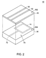
- FIG. 2 shows a structural diagram of a dual inductance structure according to an embodiment of the invention
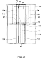
- FIG. 3 shows a top view of the dual inductance structure in FIG. 2 ;
- FIG. 4 shows a first inductance element and a second inductance element in FIG. 3 ;
- FIG. 5 shows a grounding element in FIG. 3 ;
- FIG. 6 shows an equivalent circuit diagram of the dual inductance structure in FIG. 2 ;
- FIG. 7 shows a dual inductance structure of another embodiment of the invention.
- FIG. 8A shows a structural diagram of a dual inductance structure being applied in a miniaturized bandpass filter
- FIG. 8B shows an equivalent circuit diagram of the miniaturized bandpass filter in FIG. 8A ;
- FIG. 8C shows the result simulating insertion loss of the miniaturized bandpass filter in FIG. 8A and FIG. 1A ;
- FIG. 9 shows a dual inductance structure of yet another embodiment of the invention.
- the invention discloses a dual inductance structure including a substrate, a first inductance element, a second inductance element and a grounding element.
- the substrate has a layout layer and a grounding layer.
- the first inductance element is disposed on the layout layer and has a first conductor and a second conductor which are connected with each other.
- the second inductance element is disposed on the layout layer and has a third conductor and a fourth conductor which are connected with each other, wherein the fourth conductor is adjacent to the second conductor.
- the grounding element is disposed on the grounding layer and has a first grounding portion and a second grounding portion which are connected with each other.
- the first grounding portion is located at an area of the grounding layer corresponding to an area between the first conductor and the third conductor. At least a part of the second grounding portion is located at an area of the grounding layer corresponding to an area between the first conductor and the second conductor, and at least another part of the second grounding portion is located of the grounding layer corresponding to an area at an area between the third conductor and the fourth conductor.
- the dual inductance structure 10 includes a substrate 30 , a first inductance element 50 , a second inductance element 52 and a grounding element 70 .
- the substrate 30 has a layout layer 302 and a grounding layer 304 .
- the first inductance element 50 is disposed on the layout layer 302 of the substrate 30 .
- the second inductance element 52 is disposed on the layout layer 302 of the substrate 30 .
- the grounding element 70 is disposed on the grounding layer 304 and has a first grounding portion 72 and a second grounding portion 74 , wherein the first grounding portion 72 and the second grounding portion 74 are connected with each other.
- the first inductance element 50 has a first conductor 502 and a second conductor 504 , wherein the first conductor 502 and the second conductor 504 are connected with each other.
- the second inductance element 52 has a third conductor 522 and a fourth conductor 524 , which are connected with each other, and the fourth conductor 524 is adjacent to the second conductor 504 .
- the first grounding portion 72 is located at an area of the grounding layer corresponding to an area F 1 , which is between the first conductor 502 and the third conductor 522 .
- At least a part of the second grounding portion 74 is located at an area of the grounding layer corresponding to an area Q 1 , which is between the first conductor 502 and the second conductor 504 , and an area Q 2 , which is between the third conductor 522 and the fourth conductor 524 .
- FIG. 4 shows a first inductance element 50 and a second inductance element 52 in FIG. 3 .
- FIG. 5 shows a grounding element 70 in FIG. 3 .
- the first conductor 502 and the second conductor 504 of the first inductance element 50 as well as the third conductor 522 and the fourth conductor 524 of the second inductance element 52 each have substantially a bar structure disposed on the layout layer 302 of the substrate 30 , wherein the first conductor 502 corresponds to the third conductor 522 , and the second conductor 504 corresponds to the fourth conductor 524 .
- the first conductor 502 is substantially parallel to the third conductor 522
- the second conductor 504 is substantially parallel to the fourth conductor 524 .
- the first conductor to the fourth conductor 502 , 504 , 522 , and 524 are exemplified by a bar structure in the present embodiment of the invention.
- the invention is not limited thereto, and the first conductor or the third conductor can have a spiral structure or any other structure.
- the first grounding portion 72 having substantially a strip structure is deposited on the grounding layer 304 , and is located at an area corresponding to the area F 1 between the first conductor 502 and the third conductor 522 .
- the second grounding portion 74 having substantially a ring structure is deposited on the grounding layer 304 , and is located at the area corresponding to an area F 2 between the second conductor 502 and the fourth conductor 522 . As indicated in FIG.
- a part 742 of the second grounding portion 74 is on the grounding layer 304 and located at the area corresponding to the area Q 1 , which is between the first conductor 502 and the second conductor 504 , and the area Q 2 , which is between the third conductor 522 and the fourth conductor 524 , and is connected to one end 722 of the first grounding portion 72 with each other.
- the grounding element 70 is disposed on the grounding layer 304 of the substrate 30 , and divides the area on which the first inductance element 50 and the second inductance element 52 are disposed into an area 12 and an area 14 .
- the first conductor 502 , the third conductor 522 and the first grounding portion 72 are located in the area 12 . Because the first grounding portion 72 is grounded and located between the first conductor 502 and the third conductor 522 , the grounding voltage provided by the first grounding portion 72 will make the mutual inductance between the first inductance element 50 and the second inductance element 52 become insignificant.
- the second conductor 504 , the fourth conductor 524 and the second grounding portion 74 are located in the area 14 , wherein the second grounding portion 74 is grounded and surrounds the second conductor 504 and the fourth conductor 524 . Because the second grounding portion 74 provides the grounding voltage and surrounds the second conductor 504 and the fourth conductor 524 , the mutual inductance between the second conductor 504 and the fourth conductor 524 is independent and is not affected by the first conductor 502 and the third conductor 522 . Thus, the mutual inductance between the first inductance element 50 and the second inductance element 52 is almost determined by the mutual inductance between the second conductor 504 and the fourth conductor 524 . Each of the second conductor 504 and the fourth conductor 524 has a self inductance. Examples will be made in the following for illustration.
- the first inductance element L 1 has a first predetermined inductance L 1
- the second inductance element L 2 has a second predetermined inductance L 2
- the first grounding portion 72 is grounded and located between the first conductor 502 and the third conductor 522 , the first conductor 502 and the third conductor 522 generate a mutual inductance effect satisfies with the equation Lm 1 ⁇ 0. Because the second grounding portion 74 is grounded and surrounds the second conductor 504 and the fourth conductor 524 , the mutual inductance Lm 2 generated from the second conductor 504 and the fourth conductor 524 is not equal to 0, but satisfies with the equation
- Lm ⁇ ⁇ 2 K ⁇ ⁇ L ⁇ ⁇ 2 ⁇ a * L ⁇ ⁇ 2 ⁇ b , where K is a mutual inductance effect coefficient.
- the mutual inductance Lm being predetermined can thus be satisfied, that is, Lm 2 ⁇ Lm, where the mutual inductance Lm 2 is not affected by the first conductor 502 and the third conductor 522 .
- the second grounding portion of the grounding element in the present embodiment is not limited to have a ring structure, it may also be designed to have a bar structure.
- the second grounding portion may only have a part 742 of the second grounding portion 74 in the present embodiment, so as to make the grounding element substantially have a T-shaped structure.
- the first conductor 502 and the third conductor 522 are separated by a distance D 1 .
- the second conductor 504 has a first length A 1 and is separated from the fourth conductor 524 by a distance D 2 .
- the fourth conductor 524 has a second length A 2 .
- the first length A 1 and the second length A 2 are respectively related to the self inductances of the second conductor 504 and the fourth conductor 524 , and are substantially related to the mutual inductance value between the first inductance element 50 and the second inductance element 52 .
- the distance D 2 is also related to the mutual inductance value between the first inductance element 50 and the second inductance element 52 .
- the second grounding portion 74 has a width A 3 and a length A 4 .
- the width A 3 is preferably larger than the distance D 2 between the second conductor 504 and the fourth conductor 524 .
- the length A 4 is preferably larger than or equal to the first length A 1 of the second conductor 504 and the second length A 2 of the fourth conductor 524 .
- the distance D 1 between the first conductor 502 and the third conductor 504 is substantially equal to the distance D 2 between the second conductor 522 and the fourth conductor 524 .
- FIG. 6 an equivalent circuit diagram of the dual inductance structure in FIG. 2 is shown.
- the first inductance element 50 can be equivalent to inductance L 3
- the second inductance element 52 can be equivalent to an inductance L 4 .
- the mutual inductance value between the first inductance element 50 and the second inductance element 52 is M.
- the mutual inductance value M is related to the distance D 2 . According to the prior arts indicated in FIG.
- the miniaturized bandpass filter 100 if a smaller mutual inductance value is need and the self inductance of the inductances L 1 and L 2 is need to be maintained at the same time, it is needed to increase the distance W 1 to reduce the mutual inductance between the inductance L 1 and the inductance L 2 so as to obtain a reduced mutual inductance value.
- the above practice increases the area of the circuit layout and reduces the available space of electronic device.
- the mutual inductance value M between the first inductance element 50 and the second inductance element 52 of the dual inductance structure is substantially determined by the second conductor 504 and the fourth conductor 524 .
- the mutual inductance value M can be reduced by directly shortening the length A 1 of the second conductor 504 and the length A 2 of the fourth conductor 524 without increasing the distance D 2 . That is, the length A 4 of the second grounding portion 74 is shortened.
- the present embodiment can obtain the same level of mutual inductance value with a reduced distance D 2 , hence reducing the required area and increasing the available space of an electronic device. Besides, the required inductance value can be easily adjusted.
- the self inductances of the first inductance element 50 and the second inductance element 52 can be flexibly adjusted by way of adjusting the length T 1 of the first conductor 502 and the length T 2 of the third conductor 522 , respectively.
- the dual inductance structure 10 has wider application.
- the dual inductance structure 10 A includes a substrate 30 A, a first inductance element 50 A, a second inductance element 52 A and a grounding element 70 A.
- the first inductance element 50 A has a first conductor 502 A and a second conductor 504 A.
- the second inductance element 52 A has a third conductor 522 A and a fourth conductor 524 A.
- FIG. 7 differs with FIG. 2 in that a part of the first conductor 502 A and the third conductor 522 A each substantially have a spiral structure.
- a part 1002 of the first conductor 502 A and a part 1004 of the third conductor 522 A each have substantially a spiral structure or even a structure of any other shapes.
- the overall lengths of the first conductor 502 A and the third conductor 522 A are respectively increased so as to increase or reduce the equivalent inductance value of the dual inductance structure 10 A, especially the equivalent self inductance.
- the structure in this embodiment also saves the area occupied by the dual inductance structure 10 A.
- the dual inductance structure 10 A further includes a fifth conductor 506 A of the first inductance element 50 A, a sixth conductor 526 A of the second inductance element 52 A, and an extension portion 75 A of the grounding element 70 A.
- the fifth conductor 506 A, the sixth conductor 526 A, and the extension portion 75 A of the grounding element 70 A are located in the area 16 .
- the area 16 substantially generates the same effect as that generated by the area 12 of FIG. 3 , which is not repeated here.
- the area 16 can be used for increasing the equivalent inductance value of the dual inductance structure 10 A, especially the equivalent self inductance.
- FIG. 8A shows a structural diagram of a dual inductance structure being applied in a miniaturized bandpass filter.
- FIG. 8B shows an equivalent circuit diagram of the miniaturized bandpass filter of FIG. 8A .
- the miniaturized bandpass filter 80 includes a dual inductance structure 10 A, an input port PORT 3 , an output port PORT 4 , a conductor 802 , a conductor 804 and a conductor 806 .
- the conductor 802 is equivalent to the capacitor C 3
- the conductor 804 is equivalent to the capacitor C 4
- the conductor 806 is equivalent to the capacitor Cp 1
- the input port PORT 3 is equivalent to the input port P 3
- the output port PORT 4 is equivalent to the output port P 4 .
- the result simulating insertion loss of the miniaturized bandpass filter in FIG. 8A and FIG. 1A is shown.
- the curve 808 of insertion loss S( 3 , 4 ) of the miniaturized bandpass filter is close to the curve 810 of insertion loss S( 1 , 2 ) of the miniaturized bandpass filter, wherein 1 to 4 denote PORT 1 to PORT 4 , respectively.
- the miniaturized bandpass filter of the embodiment not only achieves a similar bandpass effect, but also reduces the area of the circuit layout.
- the dual inductance structure 10 B includes a first inductance element 50 B, a second inductance element 52 B and a grounding element 70 B.
- the grounding element 70 B includes a first grounding portion 72 B and a second grounding portion 74 B.
- FIG. 9 differs with FIG. 2 in that the grounding element 70 B further includes a third grounding portion 76 B, which is connected to a part 742 B of the second grounding portion 74 B and surrounds the first conductor 502 B and the third conductor 522 B.
- the dual inductance structure 10 B of the present embodiment is disposed in an environment where the dual inductance structure 10 B is surrounded by other elements, this embodiment can prevent the dual inductance structure 10 B from being electrically interferenced by other elements.
- the first conductor 502 B of the first inductance element 50 B and the third conductor 524 B of the second inductance element 52 B each can also have a spiral structure as well.
- the dual inductance structure of the invention reduces the layout area and enables the electronic device using the same to achieve the objectives of lightweight, slimness and compactness, so that the market competitiveness thereof can thus be increased.
Landscapes
- Physics & Mathematics (AREA)
- Electromagnetism (AREA)
- Filters And Equalizers (AREA)
Abstract
Description
where K is a mutual inductance effect coefficient. Thus, the mutual inductance Lm being predetermined can thus be satisfied, that is, Lm2≅Lm, where the mutual inductance Lm2 is not affected by the
Claims (13)
Priority Applications (1)
| Application Number | Priority Date | Filing Date | Title |
|---|---|---|---|
| US12/427,962 US7808357B2 (en) | 2008-09-10 | 2009-04-22 | Dual inductance structure |
Applications Claiming Priority (5)
| Application Number | Priority Date | Filing Date | Title |
|---|---|---|---|
| US13650408P | 2008-09-10 | 2008-09-10 | |
| TW098104390A TWI365463B (en) | 2008-09-10 | 2009-02-11 | Dual inductance structure |
| TW98104390A | 2009-02-11 | ||
| TW98104390 | 2009-02-11 | ||
| US12/427,962 US7808357B2 (en) | 2008-09-10 | 2009-04-22 | Dual inductance structure |
Publications (2)
| Publication Number | Publication Date |
|---|---|
| US20100060403A1 US20100060403A1 (en) | 2010-03-11 |
| US7808357B2 true US7808357B2 (en) | 2010-10-05 |
Family
ID=41798745
Family Applications (1)
| Application Number | Title | Priority Date | Filing Date |
|---|---|---|---|
| US12/427,962 Active US7808357B2 (en) | 2008-09-10 | 2009-04-22 | Dual inductance structure |
Country Status (1)
| Country | Link |
|---|---|
| US (1) | US7808357B2 (en) |
Families Citing this family (1)
| Publication number | Priority date | Publication date | Assignee | Title |
|---|---|---|---|---|
| US8922309B1 (en) * | 2011-10-17 | 2014-12-30 | Xilinx, Inc. | Devices and methods for tuning an inductor |
Citations (9)
| Publication number | Priority date | Publication date | Assignee | Title |
|---|---|---|---|---|
| US6404319B1 (en) * | 1999-08-25 | 2002-06-11 | Murata Manufacturing, Co., Ltd. | Variable inductance element |
| US6577219B2 (en) | 2001-06-29 | 2003-06-10 | Koninklijke Philips Electronics N.V. | Multiple-interleaved integrated circuit transformer |
| US6798326B2 (en) | 2001-08-01 | 2004-09-28 | Sony Corporation | Inductor element and integrated circuit employing inductor element |
| US20070013462A1 (en) * | 2005-07-15 | 2007-01-18 | Delta Electronics, Inc. | Dual-band bandpass filter |
| US7227428B2 (en) * | 2002-10-29 | 2007-06-05 | Tdk Corporation | RF module and mode converting structure having magnetic field matching and penetrating conductor patterns |
| US7321284B2 (en) * | 2006-01-31 | 2008-01-22 | Tdk Corporation | Miniature thin-film bandpass filter |
| US7518473B2 (en) * | 2007-05-09 | 2009-04-14 | Chi-Liang Ni | Methods for designing switchable and tunable broadband filters using finite-width conductor-backed coplanar waveguide structures |
| US7538652B2 (en) * | 2006-08-29 | 2009-05-26 | International Business Machines Corporation | Electrical component tuned by conductive layer deletion |
| US7602264B2 (en) * | 2005-07-13 | 2009-10-13 | Kyocera Corporation | Filter device, multiband filter, duplexer and communications equipment using the filter device |
-
2009
- 2009-04-22 US US12/427,962 patent/US7808357B2/en active Active
Patent Citations (9)
| Publication number | Priority date | Publication date | Assignee | Title |
|---|---|---|---|---|
| US6404319B1 (en) * | 1999-08-25 | 2002-06-11 | Murata Manufacturing, Co., Ltd. | Variable inductance element |
| US6577219B2 (en) | 2001-06-29 | 2003-06-10 | Koninklijke Philips Electronics N.V. | Multiple-interleaved integrated circuit transformer |
| US6798326B2 (en) | 2001-08-01 | 2004-09-28 | Sony Corporation | Inductor element and integrated circuit employing inductor element |
| US7227428B2 (en) * | 2002-10-29 | 2007-06-05 | Tdk Corporation | RF module and mode converting structure having magnetic field matching and penetrating conductor patterns |
| US7602264B2 (en) * | 2005-07-13 | 2009-10-13 | Kyocera Corporation | Filter device, multiband filter, duplexer and communications equipment using the filter device |
| US20070013462A1 (en) * | 2005-07-15 | 2007-01-18 | Delta Electronics, Inc. | Dual-band bandpass filter |
| US7321284B2 (en) * | 2006-01-31 | 2008-01-22 | Tdk Corporation | Miniature thin-film bandpass filter |
| US7538652B2 (en) * | 2006-08-29 | 2009-05-26 | International Business Machines Corporation | Electrical component tuned by conductive layer deletion |
| US7518473B2 (en) * | 2007-05-09 | 2009-04-14 | Chi-Liang Ni | Methods for designing switchable and tunable broadband filters using finite-width conductor-backed coplanar waveguide structures |
Also Published As
| Publication number | Publication date |
|---|---|
| US20100060403A1 (en) | 2010-03-11 |
Similar Documents
| Publication | Publication Date | Title |
|---|---|---|
| US7982557B2 (en) | Layered low-pass filter capable of producing a plurality of attenuation poles | |
| CN101673618B (en) | Dual Inductor Structure | |
| US9077061B2 (en) | Directional coupler | |
| KR100753319B1 (en) | Duplexer | |
| US6566986B2 (en) | Dielectric filter | |
| US9947979B2 (en) | High-frequency filter and electronic device | |
| US10957959B2 (en) | Band-pass filter | |
| US20180226934A1 (en) | Band-pass filter | |
| US7649431B2 (en) | Band pass filter | |
| US10242792B2 (en) | Multilayer electronic component | |
| US6750741B2 (en) | Band pass filter | |
| US7808357B2 (en) | Dual inductance structure | |
| US6922126B1 (en) | Inductor element | |
| US6498587B1 (en) | Compact patch antenna employing transmission lines with insertable components spacing | |
| US7369018B2 (en) | Dielectric filter | |
| JPH0153521B2 (en) | ||
| US7839253B2 (en) | Coupled inductor structure | |
| US6765459B2 (en) | Laminated dielectric resonator and laminated dielectric filter | |
| US7800465B2 (en) | Passive component | |
| JP4669722B2 (en) | Resonant circuit, filter circuit, multilayer substrate and circuit module | |
| US9831555B2 (en) | Antenna device | |
| JP2007128939A (en) | High-frequency module | |
| JP2003258547A (en) | Antenna device | |
| EP1587135A1 (en) | Helical inductor | |
| US7005949B2 (en) | Dielectric filter |
Legal Events
| Date | Code | Title | Description |
|---|---|---|---|
| AS | Assignment |
Owner name: ADVANCED SEMICONDUCTOR ENGINEERING, INC.,TAIWAN Free format text: ASSIGNMENT OF ASSIGNORS INTEREST;ASSIGNORS:SHYU, YING-CHIEH;LEE, PAO-NAN;CHEN, CHI-HAN;REEL/FRAME:022582/0816 Effective date: 20090411 Owner name: ADVANCED SEMICONDUCTOR ENGINEERING, INC., TAIWAN Free format text: ASSIGNMENT OF ASSIGNORS INTEREST;ASSIGNORS:SHYU, YING-CHIEH;LEE, PAO-NAN;CHEN, CHI-HAN;REEL/FRAME:022582/0816 Effective date: 20090411 |
|
| STCF | Information on status: patent grant |
Free format text: PATENTED CASE |
|
| FPAY | Fee payment |
Year of fee payment: 4 |
|
| MAFP | Maintenance fee payment |
Free format text: PAYMENT OF MAINTENANCE FEE, 8TH YEAR, LARGE ENTITY (ORIGINAL EVENT CODE: M1552) Year of fee payment: 8 |
|
| MAFP | Maintenance fee payment |
Free format text: PAYMENT OF MAINTENANCE FEE, 12TH YEAR, LARGE ENTITY (ORIGINAL EVENT CODE: M1553); ENTITY STATUS OF PATENT OWNER: LARGE ENTITY Year of fee payment: 12 |