US7795807B2 - Organic light emitting display - Google Patents
Organic light emitting display Download PDFInfo
- Publication number
- US7795807B2 US7795807B2 US11/379,234 US37923406A US7795807B2 US 7795807 B2 US7795807 B2 US 7795807B2 US 37923406 A US37923406 A US 37923406A US 7795807 B2 US7795807 B2 US 7795807B2
- Authority
- US
- United States
- Prior art keywords
- sub
- oled
- substrate
- antireflective layer
- pixel
- Prior art date
- Legal status (The legal status is an assumption and is not a legal conclusion. Google has not performed a legal analysis and makes no representation as to the accuracy of the status listed.)
- Active, expires
Links
Images


Classifications
-
- H—ELECTRICITY
- H10—SEMICONDUCTOR DEVICES; ELECTRIC SOLID-STATE DEVICES NOT OTHERWISE PROVIDED FOR
- H10K—ORGANIC ELECTRIC SOLID-STATE DEVICES
- H10K59/00—Integrated devices, or assemblies of multiple devices, comprising at least one organic light-emitting element covered by group H10K50/00
- H10K59/10—OLED displays
- H10K59/12—Active-matrix OLED [AMOLED] displays
-
- H—ELECTRICITY
- H10—SEMICONDUCTOR DEVICES; ELECTRIC SOLID-STATE DEVICES NOT OTHERWISE PROVIDED FOR
- H10K—ORGANIC ELECTRIC SOLID-STATE DEVICES
- H10K50/00—Organic light-emitting devices
- H10K50/80—Constructional details
- H10K50/86—Arrangements for improving contrast, e.g. preventing reflection of ambient light
- H10K50/865—Arrangements for improving contrast, e.g. preventing reflection of ambient light comprising light absorbing layers, e.g. light-blocking layers
-
- H—ELECTRICITY
- H10—SEMICONDUCTOR DEVICES; ELECTRIC SOLID-STATE DEVICES NOT OTHERWISE PROVIDED FOR
- H10K—ORGANIC ELECTRIC SOLID-STATE DEVICES
- H10K59/00—Integrated devices, or assemblies of multiple devices, comprising at least one organic light-emitting element covered by group H10K50/00
- H10K59/80—Constructional details
- H10K59/8791—Arrangements for improving contrast, e.g. preventing reflection of ambient light
- H10K59/8792—Arrangements for improving contrast, e.g. preventing reflection of ambient light comprising light absorbing layers, e.g. black layers
Definitions
- This invention relates to an organic light emitting display (OLED), and more particularly, to an OLED with a high contrast ratio on the display screen and a longer life time.
- OLED organic light emitting display
- an OLED being developed later than a liquid crystal display (LCD)
- LCD liquid crystal display
- beneficial characteristics such as having a spontaneous light source, a wide viewing angle, high response velocity, power saving, strong contrast, high brightness, small thickness, full-color, simpler structure, and a wide operating temperature
- the OLED has been used extensively in small and medium scale portable display fields.
- the conductors, electrodes, or other patterns made of metal in the OLED may reflect lights, its display images often has low quality caused by its unfavorable contrast ratio when the OLED is operated in an environment with strong ambient light.
- a polarizer is placed on the surface of the substrate of the OLED to reduce the reflection of the ambient light.
- the polarizer may reduce the reflection of the ambient light effectively, at the mean time the penetration rate of the light produced by the OLED itself may be reduced to 42%, which causes the insufficient luminous efficiency.
- high voltage has to be provided to the organic emitting elements to increase their luminosity.
- the prior method of setting up a polarizer on the surface of the substrate still has its shortcoming which is that it cannot meet both the contrast ratio and luminosity requirement and the low power consumption requirement of the display.
- an OLED has a first substrate, a second substrate opposite to and under the first substrate, a plurality of organic emitting elements disposed in each of the sub-pixels, and an antireflective layer formed in each sub-pixel.
- the ratio of the area of the antireflective layer to the area of the sub-pixel is between about 60% and about 87%.
- the OLED comprises a first substrate, a second substrate parallel and opposite to the first substrate, having a plurality of sub-pixels, a plurality of organic emitting elements and an antireflective layer in each of the sub-pixels, wherein the ratio of the area of the antireflective layer to the area of the sub-pixel is defined as the anti-reflect/sub-pixel ratio.
- This method comprises determining a first relation equation between the relative life time of the organic emitting elements and the anti-reflect/sub-pixel ratio based on the characteristics of the organic emitting elements, and then determining a second relation equation between the contrast ratio of the OLED and the anti-reflect/sub-pixel ratio based on the characteristics of the OLED. Then, a predetermined minimum value of the contrast ratio and a predetermined minimum value of the relative life time value are chosen to be used in the first relation equation and the second relation equation to calculate a preset range of the anti-reflect/sub-pixel ratio.
- the portion in each sub-pixel which is occupied by the antireflective layer is designed to make the contrast ratio of the OLED equal to or more than the predetermined minimum value of the contrast ratio and to allow the relative life time of each organic emitting element in the OLED equal to or more than the predetermined minimum value of the relative life time value.
- an optimal range of the anti-reflect/sub-pixel ratio may be designed to satisfy the contrast ratio requirement of the OLED in the industry without reducing the life time of the organic emitting elements. And even a longer life time of each organic emitting elements can be provided according to the claimed invention.
- FIG. 1 is a side cross-section schematic diagram of an OLED of this invention.
- FIG. 2 is an enlarged schematic diagram of the sub-pixel of the OLED shown in FIG. 1 .
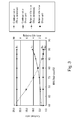
- FIG. 3 is a curve diagram of the relationship of the anti-reflective/sub-pixel ratio versus the relative life time of organic emitting elements and the contrast ratio.
- FIG. 1 is a side cross-section schematic diagram of an OLED 10 of this invention.
- the OLED 10 of this invention comprises a first substrate 11 and a second substrate 12 , wherein the first substrate 11 and the second substrate 12 are parallel to each other and jointed by sealant (not shown in the figure) to maintain a fixed spacing between them.
- the OLED 10 is a rear emission type panel. Therefore, the surface 12 a of the second substrate 12 facing away from the first substrate 11 is the display surface 12 a of the OLED 10 .
- the second substrate 12 is made of transparent materials such as glass, plastic, quartz, or other transparent materials.
- the first substrate 11 may be made of either transparent materials or non-transparent materials.
- the second substrate 12 comprises a plurality of sub-pixels 40 , each of which comprises an organic emitting element 46 , a thin film transistor (TFT), an antireflective layer, and other thin film layers.
- TFT thin film transistor
- each layer of materials on the second substrate 12 will be introduced from bottom to top according to the structure of the side cross-section of the OLED 10 .
- An antireflective layer 14 is positioned on the surface of the second substrate 12 close to the first substrate 11 , and it has an opening 14 a .
- the antireflective layer 14 is a black matrix (BM) which may absorb the ambient light propagating into the OLED 10 through the display surface 12 a and prevent the influence of the reflection of the ambient light on the contrast ratio of the display images of the OLED 10 .
- the material of the BM may be chrome, chromic oxide and chromic nitride, or other materials which have good quality of antireflection. It is preferred that the antireflective rate of the BM is less than 7%.
- the portion in the sub-pixel 40 which has the antireflective layer 14 is defined as a non-emitting region 44 and the portion in this sub-pixel 40 without the antireflective layer 14 (the opening 14 a of the antireflective layer 14 ) is defined as an emitting region 42 .
- a non-conductive buffer layer 15 covers the surface of the antireflective layer 14 .
- a transistor is placed comprising a gate 24 , a gate dielectric layer 16 , a drain 18 , a source 20 , and a semiconductor layer 22 serving as the channel of the transistor.
- a conductive layer 28 is positioned on the drain 18 and the source 20 to connect a data line (not shown in the figure) and the pixel electrode 32 respectively. Since the materials of the transistor and the conductive layer 28 usually comprise conductive materials with the property of antireflection, such as metal, the transistor and conductive layer 28 in this invention are placed directly above the antireflective layer 14 to prevent the transistor and the conductive layer from reflecting ambient light.
- a first inter-layer dielectric layer 26 is on the gate dielectric layer 16 , and a second inter-layer dielectric layer 30 and a non-conductive planar layer 34 are placed in the non-emitting region 44 above the conductive layer 28 , wherein the first inter-layer dielectric layer 26 and the second inter-layer dielectric layer 30 may be made of silicon nitride (SiN x ), silicon oxide (SiO x ), tetra-ethyl-ortho-silicate (TEOS), or other non-conductive organic or inorganic materials, and the material of the planar layer 34 may be organic materials, such as acrylic resin, or the materials described above for the inter-layer dielectric layers.
- the organic emitting elements 46 are placed on top of the above-described non-conductive layers and in the emitting region 42 of each sub-pixel 40 .
- the organic emitting element 46 comprises a pixel electrode 32 as the anode, an organic emitting layer 36 , and a cathode 38 .
- the material of the pixel electrode 32 is preferred to comprise transparent metal oxides, such as Indium-tin-oxide (ITO) or Indium-zinc-oxide (IZO).
- the cathode 38 is preferred to comprise materials with high reflective property, such as aluminum, Ag, alum or Ag alloy or other metal materials to reflect the light from the organic emitting layer 36 for increasing the luminosity.
- the organic emitting layer 36 comprises a hole transporting layer, an emitting layer, and an electron transporting layer, and it is actuated by the pixel electrode 32 and the cathode 38 to emit lights. Therefore, the antireflective layer 14 is disposed between the transistors and the substrate 12 , and the transistors are disposed between the organic emitting elements 46 and the antireflective layer 14 .
- FIG. 2 is the placement schematic diagram of the sub-pixel 40 of the OLED 10 shown in FIG. 1 .
- the opening 14 a of the anti-reflective layer 14 is the emitting region 42 of the sub-pixel 40
- the portion of the sub-pixel 40 comprising the antireflective layer 14 is defined as the non-emitting region 44 .
- the non-emitting region 44 /sub-pixel 40 area ratio is about 60% to 87%, preferable about 70% to 87%.
- the non-emitting region 44 /sub-pixel 40 area ratio may be different or not completely the same in each sub-pixel to create the best performance of the display images.
- the antireflective layer 14 placed between the organic emitting elements 46 and the display surface 12 a must occupy certain area (i.e. the area of the non-emitting region) to absorb sufficient ambient lights for preventing the contrast ratio of the display images from being reduced by the cathode 38 reflecting ambient lights.
- the non-emitting region 44 occupies a large area of the sub-pixel 40
- the antireflective layer 14 may also shield relatively a large amount of the light produced by the organic emitting elements 46 , which causes the entire luminosity of the display images of the OLED 10 reduced.
- a conventional method is to provide more electric current to the organic emitting elements 46 to increase its luminous efficiency.
- the characteristic of this invention is to provide a method to determine the optimal area ratio of the non-emitting region 44 to the sub-pixel 40 (i.e. antireflective layer/sub-pixel area ratio or anti-reflect/sub-pixel ratio).
- FIG. 3 is a curve diagram of the relationship of the antireflective layer/sub-pixel ratio (i.e. the BM/sub-pixel ratio) versus the relative life time of the organic emitting elements and the contrast ratio.
- Curves A 1 and A 2 are the estimate relation curves of the contrast ratio of the OLED 10 and the relative life time of the organic emitting elements 46 respectively versus the BM/sub-pixel ratio of the OLED 10 in this invention.
- Curves B 1 and B 2 are the relation curves of the contrast ratio and the relative life time of the organic emitting elements respectively versus the BM/sub-pixel ratio of the OLED according to the prior art with a polarizer, which are used as a comparison to this invention, wherein the penetration rate of the polarizer of the OLED according to the prior art is 42%.
- C.R.” is defined as the contrast ratio of the display
- I on represents the luminosity of the display while it is on its full luminosity, which means the sum of the maximum luminosity of the display and the luminosity of the reflected ambient light
- I off represents the luminosity of the display while it is in complete darkness, which means the luminosity of the reflected ambient light.
- T 1 and T 2 respectively represent the luminosities of the organic emitting elements 46 with different electric currents
- L 1 and L 2 respectively represent the life time of the organic emitting elements 46 under the conditions of T 1 and T 2
- r is defined as the acceleration factor for the life time of the organic emitting elements 46 .
- the method of this invention compares life time of the organic emitting elements and the contrast ratio of OLEDs known in the prior art, and uses the curves A 1 and A 2 to determine the optimal range of the BM/sub-pixel ratio of the OLED of this invention. For example, a contrast ratio above 3.0 is generally acceptable, wherein a contrast ratio of 5.0 is preferred. Therefore, to design an OLED with the minimum contrast ratio of 3.0 and the life time of the organic emitting elements not shorter than that of the prior art OLED, find the point of 3.0 on the vertical axis in the left side of FIG. 3 , move horizontally to meet the curve A 1 , and the BM/sub-pixel ratio corresponding to the contrast ratio of 3.0 is found to be 60%.
- the preferred area ratio of the non-emitting region 44 to the sub-pixel 40 of this invention OLED 10 is between about 70% and 87%. Based on the previous explanation, those skilled in the art shall realize that while designing the area ratio of the non-emitting region 44 to the sub-pixel 40 , we may estimate a relation equation between the area ratio of the non-emitting region to the sub-pixel and the contrast ratio under a predetermined ambient light and based on the characteristics of the displays, to determine the a preferable reset range of the area ratio non-emitting region to the sub-pixel.
- the application of this invention is not limited to the rear emission type structure of the OLED as in FIG. 1 . It may be applied to other displays with different structures such as top emission type OLED or displays with color filters.
- this invention provides an OLED which does not require a polarizer but provides high contrast ratio by adjusting the design of the antireflective layer (non-emitting)/sub-pixel area ratio. Since this invention OLED does not contain the polarizer with penetration rate under 50%, high voltage for the organic emitting elements to increase the luminosity is not required, which furthermore increases the life time of the organic emitting elements to allow the OLED of this invention to have both good contrast ratio and long life time.
Landscapes
- Engineering & Computer Science (AREA)
- Microelectronics & Electronic Packaging (AREA)
- Physics & Mathematics (AREA)
- Optics & Photonics (AREA)
- Electroluminescent Light Sources (AREA)
Abstract
Description
C.R.=I on /I off (a)
(T 2 /T 1)=(L 1 /L 2)r (b)
Claims (15)
Applications Claiming Priority (3)
| Application Number | Priority Date | Filing Date | Title |
|---|---|---|---|
| TW094139404A TWI299239B (en) | 2005-11-10 | 2005-11-10 | Organic light emitting display |
| TW094139404 | 2005-11-10 | ||
| TW94139404A | 2005-11-10 |
Publications (2)
| Publication Number | Publication Date |
|---|---|
| US20070103061A1 US20070103061A1 (en) | 2007-05-10 |
| US7795807B2 true US7795807B2 (en) | 2010-09-14 |
Family
ID=38003058
Family Applications (1)
| Application Number | Title | Priority Date | Filing Date |
|---|---|---|---|
| US11/379,234 Active 2027-07-13 US7795807B2 (en) | 2005-11-10 | 2006-04-19 | Organic light emitting display |
Country Status (2)
| Country | Link |
|---|---|
| US (1) | US7795807B2 (en) |
| TW (1) | TWI299239B (en) |
Cited By (4)
| Publication number | Priority date | Publication date | Assignee | Title |
|---|---|---|---|---|
| US20110260155A1 (en) * | 2006-01-05 | 2011-10-27 | Konica Minolta Holdings, Inc. | Bottom emission type organic electroluminescent panel |
| US20150001470A1 (en) * | 2013-06-28 | 2015-01-01 | Universal Display Corporation | Barrier covered microlens films |
| US20150279917A1 (en) * | 2014-03-26 | 2015-10-01 | Lg Display Co., Ltd. | Organic light emitting display |
| US9740040B2 (en) | 2013-12-27 | 2017-08-22 | Samsung Display Co., Ltd. | Display panel, display apparatus having the same and method of manufacturing the same |
Families Citing this family (6)
| Publication number | Priority date | Publication date | Assignee | Title |
|---|---|---|---|---|
| TWI284491B (en) * | 2005-10-28 | 2007-07-21 | Au Optronics Corp | Flat display panel |
| KR100829750B1 (en) * | 2006-12-06 | 2008-05-15 | 삼성에스디아이 주식회사 | Organic light emitting display |
| KR101117642B1 (en) * | 2009-11-16 | 2012-03-05 | 삼성모바일디스플레이주식회사 | Organic light emitting diode display and method for manufacturing the same |
| KR20120042520A (en) * | 2010-10-25 | 2012-05-03 | 삼성모바일디스플레이주식회사 | Organic light emitting diode display apparatus and manufacturing method thereof |
| TWI557613B (en) | 2014-11-25 | 2016-11-11 | 友達光電股份有限公司 | Touch polarizer and touch display device |
| KR102602621B1 (en) * | 2018-10-16 | 2023-11-17 | 삼성디스플레이 주식회사 | Display device |
Citations (17)
| Publication number | Priority date | Publication date | Assignee | Title |
|---|---|---|---|---|
| US5986401A (en) | 1997-03-20 | 1999-11-16 | The Trustee Of Princeton University | High contrast transparent organic light emitting device display |
| US6351066B1 (en) | 1997-10-14 | 2002-02-26 | Matsushita Electric Industrial Co., Ltd. | Organic electroluminescence element having an insulating bulkhead having an overhang portion |
| US6515428B1 (en) | 2000-11-24 | 2003-02-04 | Industrial Technology Research Institute | Pixel structure an organic light-emitting diode display device and its manufacturing method |
| US20030117071A1 (en) * | 2001-12-26 | 2003-06-26 | Samsung Sdi Co., Ltd. | Organic electroluminescent display device |
| US20030155860A1 (en) * | 2002-02-20 | 2003-08-21 | Samsung Electronics Co., Ltd. | Active matrix type organic electroluminescent display and method of manufacturing the same |
| CN1446035A (en) | 2002-03-18 | 2003-10-01 | 精工爱普生株式会社 | Organic El element and manufacturing method thereof and display device |
| TW578438B (en) | 2002-04-01 | 2004-03-01 | Kuen-Ru Juang | Organic light-emitting diode and the manufacturing method thereof |
| TW586333B (en) | 2003-05-19 | 2004-05-01 | Toppoly Optoelectronics Corp | Light-emitting device having anti-reflecting member |
| TWI223969B (en) | 2001-12-06 | 2004-11-11 | Sony Corp | Display and method of manufacturing the same |
| US6844674B2 (en) | 2002-06-12 | 2005-01-18 | Ritdisplay Corporation | Organic light emitting didode display device having light-absorbing layer |
| US6850005B2 (en) | 2002-07-25 | 2005-02-01 | Sanyo Electric Co., Ltd. | Electroluminescence display apparatus with opening in silicon oxide layer |
| TWI231723B (en) | 2004-04-16 | 2005-04-21 | Ind Tech Res Inst | Organic electroluminescence display device |
| US20050116615A1 (en) * | 2003-09-30 | 2005-06-02 | Shoichiro Matsumoto | Light emissive display device |
| US20050139834A1 (en) * | 2003-12-31 | 2005-06-30 | Jac-Yong Park | Organic electroluminescent device and fabricating method thereof |
| US20050225237A1 (en) * | 2004-04-08 | 2005-10-13 | Eastman Kodak Company | Oled microcavity subpixels and color filter elements |
| US20060038752A1 (en) * | 2004-08-20 | 2006-02-23 | Eastman Kodak Company | Emission display |
| US20070069635A1 (en) * | 2005-09-27 | 2007-03-29 | Eastman Kodak Company | OLED device having improved contrast |
-
2005
- 2005-11-10 TW TW094139404A patent/TWI299239B/en not_active IP Right Cessation
-
2006
- 2006-04-19 US US11/379,234 patent/US7795807B2/en active Active
Patent Citations (19)
| Publication number | Priority date | Publication date | Assignee | Title |
|---|---|---|---|---|
| US5986401A (en) | 1997-03-20 | 1999-11-16 | The Trustee Of Princeton University | High contrast transparent organic light emitting device display |
| US6351066B1 (en) | 1997-10-14 | 2002-02-26 | Matsushita Electric Industrial Co., Ltd. | Organic electroluminescence element having an insulating bulkhead having an overhang portion |
| US6515428B1 (en) | 2000-11-24 | 2003-02-04 | Industrial Technology Research Institute | Pixel structure an organic light-emitting diode display device and its manufacturing method |
| TWI223969B (en) | 2001-12-06 | 2004-11-11 | Sony Corp | Display and method of manufacturing the same |
| US20030117071A1 (en) * | 2001-12-26 | 2003-06-26 | Samsung Sdi Co., Ltd. | Organic electroluminescent display device |
| US20030155860A1 (en) * | 2002-02-20 | 2003-08-21 | Samsung Electronics Co., Ltd. | Active matrix type organic electroluminescent display and method of manufacturing the same |
| CN1440224A (en) | 2002-02-20 | 2003-09-03 | 三星电子株式会社 | Active matrix organic electrogenic luminating display device and manufacture thereof |
| US7135815B2 (en) | 2002-03-18 | 2006-11-14 | Seiko Epson Corporation | Organic electroluminescent device, method for manufacturing the same, and display unit |
| CN1446035A (en) | 2002-03-18 | 2003-10-01 | 精工爱普生株式会社 | Organic El element and manufacturing method thereof and display device |
| TW578438B (en) | 2002-04-01 | 2004-03-01 | Kuen-Ru Juang | Organic light-emitting diode and the manufacturing method thereof |
| US6844674B2 (en) | 2002-06-12 | 2005-01-18 | Ritdisplay Corporation | Organic light emitting didode display device having light-absorbing layer |
| US6850005B2 (en) | 2002-07-25 | 2005-02-01 | Sanyo Electric Co., Ltd. | Electroluminescence display apparatus with opening in silicon oxide layer |
| TW586333B (en) | 2003-05-19 | 2004-05-01 | Toppoly Optoelectronics Corp | Light-emitting device having anti-reflecting member |
| US20050116615A1 (en) * | 2003-09-30 | 2005-06-02 | Shoichiro Matsumoto | Light emissive display device |
| US20050139834A1 (en) * | 2003-12-31 | 2005-06-30 | Jac-Yong Park | Organic electroluminescent device and fabricating method thereof |
| US20050225237A1 (en) * | 2004-04-08 | 2005-10-13 | Eastman Kodak Company | Oled microcavity subpixels and color filter elements |
| TWI231723B (en) | 2004-04-16 | 2005-04-21 | Ind Tech Res Inst | Organic electroluminescence display device |
| US20060038752A1 (en) * | 2004-08-20 | 2006-02-23 | Eastman Kodak Company | Emission display |
| US20070069635A1 (en) * | 2005-09-27 | 2007-03-29 | Eastman Kodak Company | OLED device having improved contrast |
Cited By (8)
| Publication number | Priority date | Publication date | Assignee | Title |
|---|---|---|---|---|
| US20110260155A1 (en) * | 2006-01-05 | 2011-10-27 | Konica Minolta Holdings, Inc. | Bottom emission type organic electroluminescent panel |
| US8253132B2 (en) * | 2006-01-05 | 2012-08-28 | Konica Minolta Holdings, Inc. | Bottom emission type organic electroluminescent panel |
| US8274216B2 (en) | 2006-01-05 | 2012-09-25 | Konica Minolta Holdings, Inc. | Bottom emission type organic electroluminescent panel |
| US20150001470A1 (en) * | 2013-06-28 | 2015-01-01 | Universal Display Corporation | Barrier covered microlens films |
| US9818967B2 (en) * | 2013-06-28 | 2017-11-14 | Universal Display Corporation | Barrier covered microlens films |
| US9740040B2 (en) | 2013-12-27 | 2017-08-22 | Samsung Display Co., Ltd. | Display panel, display apparatus having the same and method of manufacturing the same |
| US20150279917A1 (en) * | 2014-03-26 | 2015-10-01 | Lg Display Co., Ltd. | Organic light emitting display |
| US9165994B1 (en) * | 2014-03-26 | 2015-10-20 | Lg Display Co., Ltd. | Organic light emitting display |
Also Published As
| Publication number | Publication date |
|---|---|
| TW200719760A (en) | 2007-05-16 |
| TWI299239B (en) | 2008-07-21 |
| US20070103061A1 (en) | 2007-05-10 |
Similar Documents
| Publication | Publication Date | Title |
|---|---|---|
| CN100385707C (en) | organic electroluminescent device | |
| US6714268B2 (en) | Pixel structure of a sunlight readable display | |
| US6897478B2 (en) | Flat panel display device with anti-reflection layer having concentration gradient | |
| US6987547B2 (en) | Liquid crystal display device | |
| US8421345B2 (en) | Electroluminescent device including white color filter pattern having blue light transmittance greater than red and green light transmittance | |
| US7638796B2 (en) | Organic light-emitting display device | |
| US8446346B2 (en) | Organic light emitting diode display | |
| KR101957547B1 (en) | Display panel | |
| US20060290274A1 (en) | Wiring substrate and display device | |
| CN100553012C (en) | organic electroluminescent device | |
| US11778880B2 (en) | Display substrate and manufacturing method thereof, display panel and display device | |
| US7795807B2 (en) | Organic light emitting display | |
| JP4271000B2 (en) | Transflective liquid crystal display device with different cell gaps | |
| US6844674B2 (en) | Organic light emitting didode display device having light-absorbing layer | |
| US10644253B2 (en) | Organic light-emitting diode display device | |
| KR101068395B1 (en) | An organic light emitting display device having a top emission type and a method of manufacturing the same | |
| JP2007227275A (en) | Organic light emitting display | |
| WO2026001472A1 (en) | Display apparatus and display panel thereof | |
| CN100426519C (en) | Pixel unit structure of self-luminous unit display with low reflectivity | |
| US8115381B2 (en) | Top-emission active matrix electroluminecient device | |
| US8188648B2 (en) | System for displaying images and method for fabricating the same | |
| US7443456B2 (en) | Dual mode liquid crystal display device with capacitor electrodes separate from pixel electrode performing and functioning as a reflection electrode | |
| KR102888573B1 (en) | Electroluminescent display device | |
| CN1776921A (en) | organic light emitting display | |
| US20240260392A1 (en) | Display apparatus |
Legal Events
| Date | Code | Title | Description |
|---|---|---|---|
| AS | Assignment |
Owner name: AU OPTRONICS CORP., TAIWAN Free format text: ASSIGNMENT OF ASSIGNORS INTEREST;ASSIGNOR:LI, SHI-HAO;REEL/FRAME:017490/0858 Effective date: 20060411 |
|
| STCF | Information on status: patent grant |
Free format text: PATENTED CASE |
|
| FPAY | Fee payment |
Year of fee payment: 4 |
|
| MAFP | Maintenance fee payment |
Free format text: PAYMENT OF MAINTENANCE FEE, 8TH YEAR, LARGE ENTITY (ORIGINAL EVENT CODE: M1552) Year of fee payment: 8 |
|
| MAFP | Maintenance fee payment |
Free format text: PAYMENT OF MAINTENANCE FEE, 12TH YEAR, LARGE ENTITY (ORIGINAL EVENT CODE: M1553); ENTITY STATUS OF PATENT OWNER: LARGE ENTITY Year of fee payment: 12 |
|
| AS | Assignment |
Owner name: NEOLAYER LLC, TEXAS Free format text: ASSIGNMENT OF ASSIGNORS INTEREST;ASSIGNOR:AUO CORPORATION;REEL/FRAME:072266/0941 Effective date: 20250701 |