US7778348B2 - Transmitter for suppressing out-of-band power for a signal - Google Patents
Transmitter for suppressing out-of-band power for a signal Download PDFInfo
- Publication number
- US7778348B2 US7778348B2 US11/867,784 US86778407A US7778348B2 US 7778348 B2 US7778348 B2 US 7778348B2 US 86778407 A US86778407 A US 86778407A US 7778348 B2 US7778348 B2 US 7778348B2
- Authority
- US
- United States
- Prior art keywords
- signal
- clipping
- clip
- input signal
- band component
- Prior art date
- Legal status (The legal status is an assumption and is not a legal conclusion. Google has not performed a legal analysis and makes no representation as to the accuracy of the status listed.)
- Expired - Fee Related, expires
Links
Images


Classifications
-
- H—ELECTRICITY
- H04—ELECTRIC COMMUNICATION TECHNIQUE
- H04L—TRANSMISSION OF DIGITAL INFORMATION, e.g. TELEGRAPHIC COMMUNICATION
- H04L27/00—Modulated-carrier systems
- H04L27/26—Systems using multi-frequency codes
- H04L27/2601—Multicarrier modulation systems
- H04L27/2614—Peak power aspects
- H04L27/2623—Reduction thereof by clipping
-
- H—ELECTRICITY
- H03—ELECTRONIC CIRCUITRY
- H03G—CONTROL OF AMPLIFICATION
- H03G11/00—Limiting amplitude; Limiting rate of change of amplitude ; Clipping in general
- H03G11/008—Limiting amplitude; Limiting rate of change of amplitude ; Clipping in general of digital or coded signals
Definitions
- the present invention relates to a transmitter used for a communication system having a high peak-to-average power ratio (PAPR).
- PAPR peak-to-average power ratio
- FIG. 1 shows a typical OFDM transmitter.
- the OFDM transmitter includes: a serial-to-parallel converter (S/P) 1 for performing serial-to-parallel conversion on an input bit stream (source of data to be transmitted); an inverse fast Fourier processor (IFFT) 2 having a size of M; a parallel-to-serial converter (P/S) 3 ; an oversampling block (interpolator) (OS) 4 ; a digital-to-analog converter (DAC) 5 ; an output low-pass filter (LPF) 6 ; an RF up converter (RF) 7 ; and a high-power amplifier (HPA) 8 that operates in class A or class A-B.
- S/P serial-to-parallel converter
- IFFT inverse fast Fourier processor
- P/S parallel-to-serial converter
- OS oversampling block
- DAC digital-to-analog converter
- LPF output low-pass filter
- RF RF up converter
- HPA high
- the OFDM transmitter shown in FIG. 1 generates an OFDM signal having a high PAPR level.
- the amplifier of this type is low in power efficiency.
- the simplest approach to reducing a PAPR of the OFDM signal is to clip (cut out) high amplitude peaks thereof.
- a variety of clipping techniques have been proposed. In some of the techniques, outputs of an inverse fast Fourier transform (IFFT) are clipped before interpolation (oversampling (OS)).
- IFFT inverse fast Fourier transform
- OS oversampling
- the signal must be interpolated before digital-to-analog conversion, thus causing peak re-growth.
- the signal may be clipped after interpolation.
- such the scheme causes extremely significant out-of-band power.
- FIG. 2 shows a configuration example of an OFDM transmitter (conventional example) to which the PAPR reducing scheme using a “clipping and filtering method” is applied.
- the OFDM transmitter shown in FIG. 2 is provided with: an IFFT 9 in place of the IFFT 2 shown in FIG. 1 ; a limiter 10 to which an output (OFDM signal) from the P/S 3 is inputted; and an LPF 11 to which an output from a limiter 10 is inputted, the LPF 11 being connected to the DAC 5 .
- an input vector (input bit stream) is converted from a frequency domain to a time domain by using an oversize IFFT 9 .
- an oversampling factor of the IFFT 9 is K
- the input vector is extended by adding M ⁇ (K ⁇ 1) zeros in the middle of the vector.
- trigonometric interpolation is performed in the time domain.
- the oversampled or interpolated signal is then clipped at the limiter 10 .
- hardware-limiting is applied to the amplitude of the complex values x at the IFFT output.
- A is a clipping level or a clipping ratio (CR)
- Clip(t) is a clip signal (difference between an original signal and a signal as an output from the limiter 10 )
- S(t) is an (unclipped) OFDM signal. Note that both x and y are complex values.
- the clipping ratio CR is defined as a ratio of the clipping level to mean (average) power of an unclipped baseband signal.
- the LPF 11 performs frequency-domain low-pass filtering to effect waveform shaping and reduction in out-of-band power.
- FIG. 3 shows a cumulative distribution function (CCDF) of the OFDM transmitter shown in FIG. 2 in terms of different clipping levels (CR).
- CCDF cumulative distribution function
- QPSK quadrature phase shift keying
- a plotted (dotted) graph that corresponds to an OFDM transmission scheme (OFDM transmitter) shown in FIG. 1 is indicated by “OFDM” in FIG. 3 .
- the filtering performed by the LPF 11 exhibits some peak re-growth (see FIG. 3 ). More compact CCDF is preferable in order to reduce a dynamic range of the HPA 8 and increase power efficiency of the HPA 8 .
- the clip signal is filtered in the LPF 11 .
- a filter unit is composed of a pair of larger FFT and IFFT modules.
- a filter task is based on a finite-impulse response (FIR) with 103 coefficient and recursive filters.
- the FIR is implemented by convolution summation.
- y(n) is an FIR output signal
- x(n) is an FIR input signal
- h(n) is unit samples of the FIR
- N is a length of the FIR (number of filter taps).
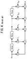
- FIG. 4 shows a structure of an FIR digital filter based on Expression 2.
- the FIR digital filter includes: a plurality of delay units for obtaining sample values from the FIR input signal x(n); a plurality of multipliers for multiplying the sample values by predetermined constants (weighting factors h 0 , h 1 , . . . , h N-1 ); and a plurality of adders for obtaining the FIR output signal y(n) by summing up outputs from the plurality of multipliers.
- the FIR digital filter may constitute an LPF or an HPF.
- the LPF 11 shown in FIG. 2 is formed of the FIR digital filter to remove out-of-band components from a main signal (to reduce out-of-band power).
- FIG. 4 shows a level of the out-of-band power suppressions (ATT) expressed in dB for a WiMAX system with 2048 subcarriers when clipping level equals 4 dB and the number of taps N of the FIR as a parameter.
- ATT out-of-band power suppressions
- the FIR digital filter In a case of implementing the FIR digital filter with an application specific integrated circuit (ASIC) implementation or a field programmable gate array (FPGA) implementation, it is necessary to provide a large number of 8-bit multipliers corresponding to the number of taps N.
- the 8-bit multiplier is about 8 times more complex than the adder.
- the conventional example has a problem in that the FIR digital filter becomes larger and more complex.
- the FIR digital filter requires more time for a low-pass filtering process.
- the present invention has an object to provide a technique capable of reducing a PAPR in a communication system employing a modulation process exhibiting a high PAPR, and capable of simplifying a filtering process for suppressing out-of-band power.
- the present invention adopts the following means in order to achieve the objects.
- the present invention provides a transmitter, including:
- a limiter performing clipping in which an amplitude part at a level higher than an amplitude level based on a predetermined clipping level is clipped from an input signal, separating the input signal into an input signal after the clipping, which contains a predetermined out-of-band component, and a clip signal clipped from the input signal through the clipping, and outputting the input signal after the clipping and the clip signal;
- a high-pass filter subjecting the clip signal inputted from the limiter to high-pass filtering for blocking an in-band component contained in the clip signal while passing an out-of-band component contained in the clip signal, which is opposite in phase to the out-of-band component contained in the input signal after the clipping;
- an adder performing an addition process on the out-of-band component received from the high-pass filter and the input signal after the clipping received from the limiter;
- an amplifier performing power amplification on a signal outputted from the adder, and outputting the amplified signal.
- the clipping performed by the limiter is followed by the high-pass filtering process for extracting the out-of-band component contained in the clip signal.
- a combining process is performed to combine a high-pass filtered output (out-of-band component) obtained through the above-mentioned high-pass filtering process with the input signal that has undergone the clipping, so the out-of-band component contained in the input signal that has undergone the clipping is canceled by the high-pass filtered output. Accordingly, by removing the out-of-band component from the input signal, it is possible to reduce (suppress) out-of-band power amplified by the amplifier, and also possible to achieve PAPR reduction.
- PAPR peak-to-average power ratio
- the clip signal contains sample values indicating amplitude values at a plurality of sample points
- the high-pass filter is configured to perform a high-pass filtering process including an addition process of adding a plurality of multiplication results after performing a multiplication process of multiplying each sample value by a predetermined weighting factor;
- the transmitter further includes a multiplication control section controlling the high-pass filter to perform the multiplication process so that the multiplication process relating to a zero sample value is avoided in the high-pass filtering process.
- the input signal after the clipping is outputted from the adder substantially without frequency distortion.
- the high-pass filter performs the multiplication process using the weighting factor only on a non-zero sample value contained in the clip signal.
- the clipping level defines the number of non-zero sample values contained in the clip signal.
- a communication system (a transmitter) employing the modulation process exhibiting a high PAPR, it is possible to reduce a PAPR and to simplify a filtering process for suppressing out-of-band power.
- FIG. 1 shows a standard OFDM transmitter.
- FIG. 2 shows a configuration example of an OFDM transmitter for implementing clipping and filtering to reduce a PAPR.
- FIG. 3 shows a graph representing a CCDF function of the OFDM transmitter (conventional example) shown in FIG. 2 .
- FIG. 4 shows a schematic diagram of a structure of an FIR digital filter.
- FIG. 5 shows a graph representing a level of an out-of-band power suppression for different numbers of taps in the FIR digital filter.
- FIG. 6 shows a table showing relationships between a clipping level CR and a zero value sample and non-zero value sample that are contained in a clip signal Clip(k).
- FIG. 7 shows a configuration example of an OFDM transmitter according to an embodiment of the present invention.
- FIG. 8A shows a spectrum (S(f)) of an original OFDM signal (main signal) inputted to the limiter.
- FIG. 8B shows a spectrum (S*(f)) of the main signal outputted from the limiter.
- FIG. 8C shows a spectrum (Clip(f)) of the clip signal Clip(k).
- FIG. 8D shows a spectrum of the clip signal that has passed the HPF.
- FIG. 8E shows a spectrum (S*(f)) of the OFDM signal that has undergone an addition process at the adder.
- FIG. 9 shows a graph representing BER performances of the OFDM signal after a clipping and filtering process at the OFDM transmitter shown in FIG. 6 .
- FIG. 10 shows a diagram of an example of the OFDM signal (main signal S(n)) to be subjected to the clipping and filtering process.
- FIG. 11 shows a diagram representing a signal (the main signal S*(n)) in which the clip signal Clip(k) is clipped from the OFDM signal shown in FIG. 10 .
- FIG. 12 shows a diagram representing the clip signal Clip(k) clipped from the OFDM signal S(n) shown in FIG. 10 .
- OFDM frequency division multiplexing
- PAPR peak-to-average power ratio
- the simplest approach to reducing the PAPR of an OFDM signal is to clip (cut out) high amplitude peaks thereof.
- LPF low-pass filter
- the LPF must have an extremely long pulse response (for example, 512 taps or more in the example of FIG. 5 ). This significantly increases the number of multiplications performed during a low-pass filtering process.
- repetitions of clipping and filtering increase the number of their operations several-fold.
- the low-pass filtering process is replaced by a set of high-pass filtering and a combination process.
- the replacement may reduce the number of total multiplications performed in a filter to approximately one-tenth or less depending on a selected clipping level. Accordingly, in a case of implementing the filter with, for example, an FPGA (Field Programmable Gate Array) implementation, it becomes possible to greatly reduce the number of FIR gates. Alternatively, in a case of implementing the FIR digital filter as software, it becomes possible to greatly reduce the number of digital signal processor (DSP) clocks. Further, it is possible to increase the number of repetitions of the “clipping and filtering” process without significant latency growth.
- FPGA Field Programmable Gate Array
- Disclosed as an embodiment of the present invention is an improvement in PAPR reduction for general OFDM-based communication systems.
- the improvement is attained by using the following techniques.
- the high-pass filtered signal is combined with a limiter output signal.
- the clip signal has non-zero values only in a case where the original OFDM signal exceeds the clipping ratio CR.
- the CCDF as shown in FIG. 3
- the probabilities exceeding the PAPR level are relatively low. Therefore, the clip signal contains a large number of zero value samples (see the table shown in FIG. 6 ) together with a few non-zero samples.
- an FIR (LPF) output represents a linear combination of an input signal (Clip(k)) with an appropriate coefficient h(k).
- h(k) the coefficient of the signal Clip(k)
- a multiplication value Clip(k) ⁇ h(k) can be obtained while omitting multiplication processes relating to all the zero value samples contained in the signal Clip(k). This case involves no penalty in out-of-band power suppression.
- FIG. 7 shows a configuration example of an OFDM transmitter applied to the OFDM communication system according to the embodiment of the present invention.
- an OFDM transmitter 100 includes: a serial-to-parallel converter (S/P) 101 to which a source of data (input bit stream) is inputted; an inverse fast Fourier processor (IFFT processor) 102 (including an oversampling block (interpolator (OS) section) based on a zero-padding IFFT or an LPF interpolator circuit); a parallel-to-serial converter (P/S) 103 ; a limiter (limiting unit) 104 having a predetermined clipping ratio CR; a high-pass filter (HPF, HPF unit) 105 ; a skip zero multiplication logic section (SZML section; multiplication control section) 106 ; and a combiner (adder, adding unit) 107 .
- the S/P 101 , the IFFT processor 102 , and the P/S 103 may be constituted by the same components as the S/P 1 , the IFFT processor 9 , and the P/S 3 shown in FIG.
- the OFDM transmitter 100 includes: a digital-to-analog converter (DAC) 108 for performing digital-to-analog conversion on a signal outputted from the adder 107 ; a low-pass filter (LPF) 109 for performing waveform shaping on a signal outputted from the DAC 108 ; an RF up converter 110 for up-converting a frequency of a signal outputted from the LPF 109 into an RF frequency; and a high power amplifier (HPA (amplifier or amplifying unit) 111 for amplifying power of a signal outputted from the RF up converter 110 to output the amplified signal.
- An output (OFDM signal) from the HPA 111 is emitted through a transmission antenna (not shown) and received by the receiver (not shown).
- the DAC 108 , the LPF 109 , the RF up converter 110 , and the HPA 111 may be constituted by the same components as the DAC 5 , the LPF 6 , the RF up converter 7 , and the HPA 8 shown in FIG. 2 , respectively.
- the limiter 104 may be constituted by the same component as the limiter 10 shown in FIG. 2 .
- the LPF 109 may be omitted.
- an original OFDM signal (main signal S(t)) outputted from the P/S 103 is inputted to the limiter 104 .
- the main signal S(t) corresponds to an OFDM signal that has undergone S/P conversion performed by the S/P 101 with respect to an input data stream, inverse Fourier transform and interpolation processing performed by the IFFT 102 , and P/S conversion performed by the P/S 103 .
- the limiter 104 operates according to a rule expressed by Expression 3. In Expression 3, CR is a clipping level.
- the clip signal (Clip(k)) that is clipped based on the clipping level CR by the limiter 104 can be expressed by Expression 4 as follows.
- the OFDM signal (S*(t)) outputted from the limiter 104 can be expressed by Expression 5 as follows.
- S *( t ) S ( t ) ⁇ Clip( t ) (5)
- the limiter 104 performs clipping on the inputted main signal S(t) based on the clipping level CR.
- the limiter 104 outputs the OFDM signal S*(t) and the clip signal Clip(t).
- the OFDM signal (main signal) S*(t) is inputted to the adder 107
- the clip signal Clip(t) is inputted to the HPF 105 .
- a high-pass filtering process performed by the HPF 105 is controlled by the SZML section 106 , and an output from the HPF 105 is inputted to the adder 107 .
- An output from the adder 107 is inputted to the DAC 108 as well as being fed back to the limiter 104 .
- FIGS. 8A to 8E show signal spectrums exhibited at different points of an OFDM system (OFDM transmitter 100 ) shown in FIG. 7 .
- FIG. 8A shows a spectrum (S(f)) of the original OFDM signal (main signal) inputted to the limiter 104 .
- FIG. 8B shows a spectrum (S*(f)) of the main signal outputted from the limiter 104 .
- FIG. 8C shows a spectrum (Clip(f)) of the clip signal Clip(k).
- FIG. 8D shows a spectrum of the clip signal that has passed the HPF 105 .
- FIG. 8E shows a spectrum (S*(f)) of the OFDM signal that has undergone an addition process at the adder 107 .
- the HPF 105 is constructed to allow the out-of-band frequencies to pass while blocking in-band frequencies ( FIG. 8D ).
- the output signal (out-of-band components) from the HPF 105 and the OFDM signal S*(k) are subjected to the addition process (combined) at the adder 107 .
- the out-of-band components of the OFDM signal S*(t) and the signal outputted from the HPF 105 are opposite in phase (have a phase difference of ⁇ ), so the out-of-band components of the OFDM signal S*(t) are canceled by the signal outputted from the HPF 105 . Accordingly, an out-of-band power level due to the out-of-band components of the OFDM signal outputted from the adder 107 becomes equal to an out-of-band power level for the original OFDM signal S(t) (before clipping). In other words, the out-of-band power is reduced (suppressed).
- the HPF 105 and the adder 107 collectively function as an LPF for removing out-of-band components from the OFDM signal S*(t) that has undergone clipping.
- the SZML section (multiplication control system) 106 functions as follows. The SZML section 106 receives the clip signal Clip(k) inputted to the HPF 105 and judges which of zero and non-zero a value (signal amplitude) of each sample contained in the clip signal represents. Most samples contained in the clip signal Clip(k) outputted from the limiter 104 have a zero value.
- the HPF 105 is implemented by the FIR digital filter as shown in FIG. 4 .
- the SZML section 106 stops or omits the multiplication process of a multiplier to which a zero sample value is to be inputted in the high-pass filtering process performed on the clip signal by the HPF 105 .
- the SZML section 106 applies an enable signal only to a multiplier to which a non-zero sample value is to be inputted, and disables an operation of the multiplier to which a zero sample value is to be inputted. This reduces the number of multiplications for high-pass filtering and simplifies the high-pass filtering process. Accordingly, the low-pass filtering process for PAPR reduction is simplified in turn.
- the SZML section 106 constructs such an FIR digital filter as to avoid the multiplication process relating to the zero sample value. This reduces the number of FIR gates and simplifies the high-pass filtering process (number of multiplications) performed by the FIR digital filter.
- the FIR digital filter is implemented by software executed by a processor (e.g., DSP) included in the HPF 105 , the processor is controlled to perform the high-pass filtering process with the multiplication process for the zero sample value being omitted.
- the SZML section 106 controls the HPF 105 to perform the multiplication process so that the multiplication process relating to the zero sample value is avoided and only the multiplication process relating to the non-zero sample value is executed. This simplifies the high-pass filtering process (multiplication process). In addition, it is possible to achieve reduction in the processor clock frequency of the processor (DSP).
- the SZML section 106 may be implemented by a computer including a processor (e.g., CPU) and a memory or by a hardware logic.
- the simplified high-pass filtering process allows reduction of a time required for the low-pass filtering performed by the HPF 105 and the adder 107 . Therefore, the clipping and filtering process (PAPR reduction process) can repeatedly be performed in a short cycle by the limiter 104 , the HPF 105 , and the adder 107 .
- the OFDM transmitter 100 does not include the SZML section 106 .
- the zero value of a sample contained in the clip signal is multiplied by the weighting factor (constant) merely to obtain zero, which simplifies the operation for the filtering.
- a load and time for the filtering process can be made lower and shorter than in the case of performing the low-pass filtering on the OFDM signal that has undergone the clipping (conventional example).
- the technique according to the embodiment of the present invention causes a significant increase in clipping noise components within a bandwidth of the OFDM signal.
- the resultant deterioration becomes smaller than expected owing to two effects.
- the reduction in constellation size is corrected by normalizing a total signal output power, which prevents an increase in bit error rate (BER)
- Second, the remaining clipping noise is added not at a receiver but at a transmitter. Therefore, in a fading channel, the clipping noise fades along with the signal. Accordingly, an influence of the clipping noise is by far smaller than that of the noise added at the receiver, which does not fade.
- FIG. 9 shows a bit error rate (BER) measured in an additive Gaussian noise (AWGN) channel in the case of adopting the OFDM transmitter 100 .
- AWGN additive Gaussian noise
- the clipping noise causes negligible (under 0.25 dB) degradation in BER. Therefore, according to the OFDM transmitter 100 , the adder 107 outputs an OFDM signal having substantially little frequency distortion, which makes it possible to suppress degradation in BER due to the clipping noise.
- the OFDM transmitter shown in FIG. 7 is implemented with high-pass filtering for PAPR reduction and out-of-band power suppression.
- the M OFDM samples of every OFDM block are independent identically-distributed Gaussian random variables. Such statistical independence is responsible for high variability of the OFDM signal, making its PAPR extremely high.
- FIG. 12 shows an amplitude of the clip signal Clip(n) outputted from the limiter 104 .
- the clip signal contains only a portion clipped from the OFDM signal S(n), so most part thereof is composed of zero value samples.
- a relative amount of samples having a non-zero amplitude i.e., ratio of non-zero value samples to the total number of samples contained in the clip signal
- the relative amount is indicated as several percent.
- the clipping level CR defines the number of non-zero samples contained in the clip signal.
- the multiplication process relating to the above-mentioned zero sample values is omitted under multiplication control of the SZML section 106 .
- the number of multiplications required for individually filtering clip signals ( FIG. 12 ) at the HPF 105 can be reduced to about one tenth of that in the case where an OFDM signal as shown in FIG. 11 is subjected to the low-pass filtering ( FIG. 2 ).
- the embodiment has been described above by illustrating the example in which the OFDM is employed as a modulation scheme for an input data stream, but the modulation scheme employed by the present invention is not limited to the OFDM. Alternatively, the present invention may be applied to transmitters adopting various modulation schemes that require power amplification.
Landscapes
- Engineering & Computer Science (AREA)
- Computer Networks & Wireless Communication (AREA)
- Signal Processing (AREA)
- Transmitters (AREA)
- Tone Control, Compression And Expansion, Limiting Amplitude (AREA)
- Amplifiers (AREA)
Abstract
Description
Clip(k)=S(k)−y(k) (4)
where y(k)=S*(k). Further, the OFDM signal (S*(t)) outputted from the
S*(t)=S(t)−Clip(t) (5)
Thus, the
Claims (7)
Applications Claiming Priority (2)
| Application Number | Priority Date | Filing Date | Title |
|---|---|---|---|
| JP2006324736A JP4653724B2 (en) | 2006-11-30 | 2006-11-30 | Transmitter that suppresses signal out-of-band power |
| JP2006-324736 | 2006-11-30 |
Publications (2)
| Publication Number | Publication Date |
|---|---|
| US20080130767A1 US20080130767A1 (en) | 2008-06-05 |
| US7778348B2 true US7778348B2 (en) | 2010-08-17 |
Family
ID=39218028
Family Applications (1)
| Application Number | Title | Priority Date | Filing Date |
|---|---|---|---|
| US11/867,784 Expired - Fee Related US7778348B2 (en) | 2006-11-30 | 2007-10-05 | Transmitter for suppressing out-of-band power for a signal |
Country Status (3)
| Country | Link |
|---|---|
| US (1) | US7778348B2 (en) |
| EP (1) | EP1928141B1 (en) |
| JP (1) | JP4653724B2 (en) |
Cited By (2)
| Publication number | Priority date | Publication date | Assignee | Title |
|---|---|---|---|---|
| US20110092173A1 (en) * | 2009-10-15 | 2011-04-21 | Crestcom, Inc. | Transmitting unit that reduces papr using out-of-band distortion and method therefor |
| US20140341315A1 (en) * | 2013-05-14 | 2014-11-20 | Intel IP Corporation | Signal peak-to-average power ratio (par) reduction |
Families Citing this family (15)
| Publication number | Priority date | Publication date | Assignee | Title |
|---|---|---|---|---|
| CN102420621B (en) * | 2011-11-16 | 2014-10-08 | 北京华力创通科技股份有限公司 | Method and device for suppressing out-of-band interference of digital signals |
| JP6077213B2 (en) * | 2012-02-03 | 2017-02-08 | 株式会社日立国際電気 | Peak reduction device |
| US8548072B1 (en) | 2012-06-20 | 2013-10-01 | MagnaCom Ltd. | Timing pilot generation for highly-spectrally-efficient communications |
| CN104769875B (en) | 2012-06-20 | 2018-07-06 | 安华高科技通用Ip(新加坡)公司 | It is transmitted using the spectral efficient of Orthogonal Frequency Division Multiplexing |
| JP5958336B2 (en) | 2012-12-28 | 2016-07-27 | 富士通株式会社 | Transmission signal power control device and communication device |
| EP2765704A1 (en) * | 2013-02-12 | 2014-08-13 | Alcatel Lucent | Method for signal conditioning in a processing apparatus and processing apparatus thereof |
| US9118519B2 (en) | 2013-11-01 | 2015-08-25 | MagnaCom Ltd. | Reception of inter-symbol-correlated signals using symbol-by-symbol soft-output demodulator |
| US20150223176A1 (en) * | 2014-02-02 | 2015-08-06 | Redline Innovations Group Inc. | Systems and methods for reducing peak to average power ratio |
| US9209848B2 (en) * | 2014-02-02 | 2015-12-08 | Redline Innovations Group Inc. | Methods and systems for dual-using a reception channel |
| US9973362B2 (en) | 2014-03-07 | 2018-05-15 | Huawei Technologies Co., Ltd. | Common broadcast channel low PAPR signaling in massive MIMO systems |
| US9496900B2 (en) | 2014-05-06 | 2016-11-15 | MagnaCom Ltd. | Signal acquisition in a multimode environment |
| US9246523B1 (en) | 2014-08-27 | 2016-01-26 | MagnaCom Ltd. | Transmitter signal shaping |
| JP6526448B2 (en) | 2015-03-05 | 2019-06-05 | 富士通株式会社 | Peak suppressor and peak suppression method |
| US9843959B2 (en) * | 2015-09-30 | 2017-12-12 | Intel IP Corporation | Interference mitigation by a scalable digital wireless modem |
| JP6608865B2 (en) * | 2017-03-17 | 2019-11-20 | 株式会社東芝 | Signal processing apparatus and method |
Citations (7)
| Publication number | Priority date | Publication date | Assignee | Title |
|---|---|---|---|---|
| JP2001189630A (en) | 1999-11-19 | 2001-07-10 | Lucent Technol Inc | Method for generating amplified signal |
| JP2002368716A (en) | 2001-06-12 | 2002-12-20 | Nippon Hoso Kyokai <Nhk> | Ofdm high efficiency power amplifier |
| US20050157812A1 (en) * | 2004-01-20 | 2005-07-21 | Der-Zheng Liu | Method and related apparatus for reducing peak-to-average-power ratio |
| US7212583B2 (en) * | 2002-11-27 | 2007-05-01 | Nokia Corporation | Transmission of signal |
| US7415251B2 (en) * | 2003-10-23 | 2008-08-19 | Samsung Electronics Co., Ltd. | Apparatus and method for improving efficiency of a power amplifier having a high peak-to-average power ratio |
| US7574189B2 (en) * | 2006-03-30 | 2009-08-11 | Fujitsu Limited | Transmitter and power amplifying method |
| US7664472B2 (en) * | 2006-02-23 | 2010-02-16 | Raytheon Company | Reducing the peak-to-average power ratio of a signal |
Family Cites Families (5)
| Publication number | Priority date | Publication date | Assignee | Title |
|---|---|---|---|---|
| WO2003075457A2 (en) * | 2002-03-01 | 2003-09-12 | Andrew Corporation | Apparatus and method for reducing peak-to-average signal power ratio |
| US20040076247A1 (en) * | 2002-10-22 | 2004-04-22 | Wiseband Communications Ltd. | Peak-to-average power ratio modifier |
| DE10320917A1 (en) * | 2003-05-09 | 2004-12-09 | Infineon Technologies Ag | Method for generating transmission signal with reduced crest factor for high bit rate data transmitting telecommunication systems, using multicarrier transmission with transmission signal containing section with at least one peak value |
| CN1993913A (en) * | 2004-08-30 | 2007-07-04 | 松下电器产业株式会社 | Peak power suppressing apparatus and peak power suppressing method |
| JP2006115096A (en) * | 2004-10-13 | 2006-04-27 | Matsushita Electric Ind Co Ltd | Multi-carrier communication apparatus and method of suppressing peak power |
-
2006
- 2006-11-30 JP JP2006324736A patent/JP4653724B2/en not_active Expired - Fee Related
-
2007
- 2007-10-05 US US11/867,784 patent/US7778348B2/en not_active Expired - Fee Related
- 2007-10-19 EP EP07118931A patent/EP1928141B1/en not_active Ceased
Patent Citations (10)
| Publication number | Priority date | Publication date | Assignee | Title |
|---|---|---|---|---|
| JP2001189630A (en) | 1999-11-19 | 2001-07-10 | Lucent Technol Inc | Method for generating amplified signal |
| US6292054B1 (en) | 1999-11-19 | 2001-09-18 | Lucent Technologies Inc. | System and method for producing an amplified signal |
| US20010035791A1 (en) | 1999-11-19 | 2001-11-01 | Lucent Technologies Inc. | System and method for producing an amplified signal |
| US6624694B2 (en) | 1999-11-19 | 2003-09-23 | Lucent Technologies Inc. | System and method for producing an amplified signal |
| JP2002368716A (en) | 2001-06-12 | 2002-12-20 | Nippon Hoso Kyokai <Nhk> | Ofdm high efficiency power amplifier |
| US7212583B2 (en) * | 2002-11-27 | 2007-05-01 | Nokia Corporation | Transmission of signal |
| US7415251B2 (en) * | 2003-10-23 | 2008-08-19 | Samsung Electronics Co., Ltd. | Apparatus and method for improving efficiency of a power amplifier having a high peak-to-average power ratio |
| US20050157812A1 (en) * | 2004-01-20 | 2005-07-21 | Der-Zheng Liu | Method and related apparatus for reducing peak-to-average-power ratio |
| US7664472B2 (en) * | 2006-02-23 | 2010-02-16 | Raytheon Company | Reducing the peak-to-average power ratio of a signal |
| US7574189B2 (en) * | 2006-03-30 | 2009-08-11 | Fujitsu Limited | Transmitter and power amplifying method |
Cited By (4)
| Publication number | Priority date | Publication date | Assignee | Title |
|---|---|---|---|---|
| US20110092173A1 (en) * | 2009-10-15 | 2011-04-21 | Crestcom, Inc. | Transmitting unit that reduces papr using out-of-band distortion and method therefor |
| US8185065B2 (en) * | 2009-10-15 | 2012-05-22 | Crestcom, Inc. | Transmitting unit that reduces PAPR using out-of-band distortion and method therefor |
| US20140341315A1 (en) * | 2013-05-14 | 2014-11-20 | Intel IP Corporation | Signal peak-to-average power ratio (par) reduction |
| US9154168B2 (en) * | 2013-05-14 | 2015-10-06 | Intel IP Corporation | Signal peak-to-average power ratio (PAR) reduction |
Also Published As
| Publication number | Publication date |
|---|---|
| JP2008141415A (en) | 2008-06-19 |
| EP1928141A3 (en) | 2011-10-12 |
| US20080130767A1 (en) | 2008-06-05 |
| EP1928141B1 (en) | 2013-02-27 |
| JP4653724B2 (en) | 2011-03-16 |
| EP1928141A2 (en) | 2008-06-04 |
Similar Documents
| Publication | Publication Date | Title |
|---|---|---|
| US7778348B2 (en) | Transmitter for suppressing out-of-band power for a signal | |
| EP1841158B1 (en) | Transmitter and power amplifying method | |
| US7839951B2 (en) | Dynamic crest factor reduction system | |
| KR101714784B1 (en) | Method and apparatus for reducing peak to average power ratio by using peak windowing | |
| US7376197B2 (en) | Signal peak reduction circuit for non-constant envelope modulation signals | |
| US8150324B2 (en) | Method and system for clipping a baseband input signal | |
| US7873116B2 (en) | Transmitter | |
| CN101068233B (en) | Method and device for reducing signal peak-to-average power ratio | |
| EP1821474B1 (en) | Signal peak voltage suppression apparatus | |
| KR101677294B1 (en) | Smoothing apparatus for peak windowing | |
| CN1716933B (en) | Method for realizing CDMA signal wave elimination | |
| EP1890388B1 (en) | Peak suppressor | |
| JP2009527988A (en) | Reduce signal peak-to-average power ratio | |
| US8654891B2 (en) | Peak suppressing apparatus, peak suppressing method and wireless communications apparatus | |
| EP3625942B1 (en) | Crest factor reduction in power amplifier circuits | |
| JP2009224922A (en) | Peak suppression apparatus, wireless transmitter, and window function generating apparatus | |
| US6922103B2 (en) | Method and apparatus for low intermodulation distortion amplification in selected bands | |
| Hammi et al. | Digital subband filtering predistorter architecture for wireless transmitters | |
| US20100310007A1 (en) | Filter Device | |
| Lee et al. | Experimental analysis of clipping and filtering effects on OFDM systems | |
| US10142136B1 (en) | Self-consistent outphasing signal separation | |
| WO2001099279A1 (en) | Signal peak reduction circuit for non-constant envelope modulation signals |
Legal Events
| Date | Code | Title | Description |
|---|---|---|---|
| AS | Assignment |
Owner name: FUJITSU LIMITED, JAPAN Free format text: ASSIGNMENT OF ASSIGNORS INTEREST;ASSIGNOR:LOZHKIN, ALEXANDER N;REEL/FRAME:019924/0568 Effective date: 20070904 |
|
| FEPP | Fee payment procedure |
Free format text: PAYOR NUMBER ASSIGNED (ORIGINAL EVENT CODE: ASPN); ENTITY STATUS OF PATENT OWNER: LARGE ENTITY |
|
| FPAY | Fee payment |
Year of fee payment: 4 |
|
| FEPP | Fee payment procedure |
Free format text: MAINTENANCE FEE REMINDER MAILED (ORIGINAL EVENT CODE: REM.) |
|
| LAPS | Lapse for failure to pay maintenance fees |
Free format text: PATENT EXPIRED FOR FAILURE TO PAY MAINTENANCE FEES (ORIGINAL EVENT CODE: EXP.); ENTITY STATUS OF PATENT OWNER: LARGE ENTITY |
|
| STCH | Information on status: patent discontinuation |
Free format text: PATENT EXPIRED DUE TO NONPAYMENT OF MAINTENANCE FEES UNDER 37 CFR 1.362 |
|
| FP | Lapsed due to failure to pay maintenance fee |
Effective date: 20180817 |