US7768332B2 - Waveform generation apparatus, setup cycle correction method and semiconductor test apparatus - Google Patents
Waveform generation apparatus, setup cycle correction method and semiconductor test apparatus Download PDFInfo
- Publication number
- US7768332B2 US7768332B2 US11/811,514 US81151407A US7768332B2 US 7768332 B2 US7768332 B2 US 7768332B2 US 81151407 A US81151407 A US 81151407A US 7768332 B2 US7768332 B2 US 7768332B2
- Authority
- US
- United States
- Prior art keywords
- cycle
- phase
- spurious noise
- clock signal
- waveform generation
- Prior art date
- Legal status (The legal status is an assumption and is not a legal conclusion. Google has not performed a legal analysis and makes no representation as to the accuracy of the status listed.)
- Expired - Fee Related, expires
Links
Images


Classifications
-
- G—PHYSICS
- G01—MEASURING; TESTING
- G01R—MEASURING ELECTRIC VARIABLES; MEASURING MAGNETIC VARIABLES
- G01R31/00—Arrangements for testing electric properties; Arrangements for locating electric faults; Arrangements for electrical testing characterised by what is being tested not provided for elsewhere
- G01R31/28—Testing of electronic circuits, e.g. by signal tracer
- G01R31/317—Testing of digital circuits
- G01R31/3181—Functional testing
- G01R31/319—Tester hardware, i.e. output processing circuits
- G01R31/31917—Stimuli generation or application of test patterns to the device under test [DUT]
- G01R31/31928—Formatter
Definitions
- the present invention relates to a waveform generation apparatus including a pattern generator, a setup cycle correction method that corrects a setup cycle of the pattern generator, and a semiconductor test apparatus including the waveform generation apparatus. More particularly, it relates to a waveform generation apparatus which moves spurious noise produced in the vicinity of a carrier in an output signal from a timing generator included in the waveform generation apparatus so as to be distant from the carrier in terms of frequency, with the result that the spurious noise can be removed by a PLL (phase locked loop) provided in the waveform generation apparatus, a setup cycle correction method, and a semiconductor test apparatus.
- PLL phase locked loop
- a semiconductor test apparatus supplies a test pattern of a frequency in accordance with an operating frequency of an electronic device to the electronic device to perform a test. Furthermore, when the electronic device as a test target has a plurality of cores having different operating frequencies, the respective cores are sequentially tested.
- the conventional semiconductor test apparatus generates a plurality of clocks in accordance with respective operating frequencies of the plurality of cores and simultaneously operates the cores based on the plurality of generated clocks to perform the test.
- FIG. 9 shows a structure of this type of multitime domain test apparatus (a waveform generation apparatus).
- the waveform generation apparatus depicted in FIG. 9 is mounted in a semiconductor test apparatus in order to perform the multitime domain test.
- a waveform generation apparatus (a semiconductor test apparatus) 100 includes a pattern generator 110 , a timing generator 120 , and a PLL 130 .
- the pattern generator 110 generates a cycle pattern based on a setup cycle.
- the timing generator 120 outputs the cycle pattern input from the pattern generator 110 as a high-precision variable clock based on a reference clock.
- the PLL (Phase Locked Loop) 130 removes spurious noise from the high-precision variable clock output from the timing generator 120 .
- the spurious noise means an unnecessary component produced in a signal (in this specification, the high-precision variable clock).
- the timing generator 120 has delay circuits 121 - 1 to 121 - n in units of the reference clock, and a high-precision variable delay circuit 122 .
- the timing generator 120 integrates a phase with respect to the reference clock every time it receives a cycle pattern signal, and switches the delay circuits 121 - 1 to 121 - n to corresponding one in real time.
- a position of the produced spurious noise with respect to a carrier can be obtained from fluctuation cycles T 1 and T 2 of the phase error depicted in FIG. 11 .
- a cycle pattern having a cycle of 8 ns is output from the pattern generator 110 , clocks which are delayed by 0 ns at first, delayed by 1 ns at second, delayed by 2 ns at third, and delayed by 3 ns at fourth with respect to the cycle pattern are output from the timing generator. Then, although a clock is delayed by 4 ns at fifth, this is the same as a reference clock cycle, and hence an amount corresponding to this cycle is subtracted, thereby delaying one cycle. That is, since a timing error fluctuates with a cycle of T 1 ⁇ 0.36 ns, spurious noise occurs at a position of 1/T 1 with respect to a fundamental frequency.
- a resolution concerning a setup cycle of the timing generator is 2 ⁇ 7 ns
- a cycle pattern having a cycle of 8 ns is output from the pattern generator 110
- a clock whose delay amount is 0 ns from the first to the (2 16 ⁇ 1) outputs is output from the timing generator 120 .
- the delay becomes 2 ⁇ 7 ns at the next 2 16 output
- a delay path varies in accordance with the cycle T 2 ⁇ 0.524 ms from the first to 2 16 output, and a phase error also fluctuates. That is, since a timing error fluctuates with the cycle of T 2 , spurious noise occurs at a position of 1/T 2 with respect to a fundamental frequency.
- the spurious noise removed by the PLL is limited to spurious noise that occurs at a position far from a carrier. That is because a loop filter of the PLL is a low-pass filter, and hence a phase fluctuation of a frequency having a higher rate is apt to be attenuated and an output hardly follows up this attenuation.
- an operating frequency is generated in accordance with each core.
- the spurious noise occurs at a position far from the carrier, e.g., a position of several-ten kHz to several-hundred kHz. Therefore, the PLL can sufficiently remove the spurious noise.
- the loop band must be subjected to trade-off in accordance with a required specification, e.g., spurious or switching characteristics, and the loop band cannot be reduced limitlessly.
- a waveform generation apparatus comprising: a pattern generator that generates a cycle pattern; a timing generator that outputs a clock signal based on the cycle pattern and a reference clock; and a phase-locked loop circuit that removes spurious noise from the clock signal, wherein the pattern generator has a cycle setter that sets a generation cycle of the clock signal as cycle data, and the cycle setter sets cycle data corrected in such a manner that the spurious noise occurs at a position where it is removable by the phase-locked loop circuit.
- the cycle data is corrected in such a manner that the spurious noise which occurs in a high-precision variable clock (the clock signal) can be removed by the phase-locked loop circuit, the spurious noise can be assuredly removed even if a high-resolution cycle is set, thereby realizing low jitters of the clock signal.
- allowing occurrence of the spurious noise at the position where this noise can be removed by the phase-lock loop circuit means allowing occurrence of the spurious noise at a position far from a carrier of the clock signal by a predetermined frequency or more.
- the cycle setter sets cycle data corrected in such a manner that a position of the spurious noise which occurs when the clock signal has the slowest cycle becomes a position where removal of the spurious noise by the phase-locked loop circuit is possible.
- the spurious noise can occur at a position where it can be removed by the phase-locked loop circuit even if a cycle of the clock signal has the lowest rate.
- the cycle setter sets cycle data corrected in such a manner that an inverse number of a cycle of a phase fluctuation which occurs in the timing generator becomes larger than a minimum value of a position where the spurious noise is removable by the phase-locked loop circuit.
- the spurious noise occurs with a value of the inverse number of the phase fluctuation cycle, the spurious noise can be produced at a position where it can be removed by the phase-locked loop circuit, thereby assuredly removing the spurious noise.
- a cycle of a reference clock that is input by the timing generator and serves as a reference for an output timing of the clock signal is determined as a reference clock cycle
- a phase of a cycle of the cycle data with respect to an integral multiple of the reference clock cycle is calculated
- the reference clock cycle is divided by the phase
- a quotient obtained by the division is multiplied by the cycle of the cycle data
- a product obtained by the multiplication is determined as a cycle of the phase modulation.
- D a minimum value of a position where the spurious noise is removable by the phase-locked loop circuit.
- the waveform generation apparatus has such a structure, setting the cycle data corrected based on a delay time with respect to the reference in the pattern generator allows occurrence of the spurious noise at a position far from the carrier, thus enabling to remove the spurious noise by the phase-locked loop circuit.
- a cycle of a reference clock that is input by the timing generator and serves as a reference for an output timing of the clock signal is determined as a reference clock cycle
- a phase of a cycle of the cycle data with respect to an integral multiple of the reference clock cycle is calculated
- a resolution concerning a setup cycle of the timing generator is divided by the phase
- a quotient obtained by the division is multiplied by the cycle of the cycle data
- a product obtained by the multiplication is determined as a cycle of the phase fluctuation.
- the waveform generation apparatus has such a structure, when a phase error fluctuates at the moment the integrated phase reaches the resolution of the timing generator, the spurious noise based on cycle properties of this phase fluctuation can be assuredly removed.
- D a minimum value of a position where the spurious noise is removable by the phase-locked loop circuit.
- the waveform generation apparatus adopts such a structure, when the cycle data corrected based on a delay time with respect to the reference is set in the pattern generator, the spurious noise occurs at a position far from the carrier, thereby removing the spurious noise by the phase-locked loop circuit.
- a setup cycle correction method of correcting cycle data that is set by a pattern generator in a waveform generation apparatus, wherein the cycle data is corrected in such a manner that spurious noise which occurs in a clock signal output from a timing generator in the waveform generation apparatus is produced at a position where the spurious noise is removable by a phase-locked loop circuit in the waveform generation apparatus, and the corrected cycle data is set in the pattern generator.
- the spurious noise occurs at a position far from the carrier, it can be removed by the phase-locked loop circuit, thereby realizing low jitters of the clock signal.
- a semiconductor test apparatus including a waveform generation apparatus that outputs a clock signal with a predetermined cycle, wherein the waveform generation apparatus is constituted of the waveform generation apparatus as described in the foregoing.
- the semiconductor test apparatus adopts such a structure, low jitters of the clock signal can be realized in the waveform generation apparatus even when this semiconductor test apparatus sets a high-resolution cycle.
- the spurious noise that occurs in the clock signal output from the timing generator in the waveform generation apparatus can be produced at a position far from the carrier, this spurious noise can be assuredly removed by the phase-locked loop circuit.
- FIG. 1 is a flowchart showing an operation of a waveform generation apparatus according to the present invention
- FIG. 2 is waveform charts showing positions where spurious noise occurs before and after correction
- FIG. 3 is a diagram showing an example of an input to a cycle setter
- FIG. 4 is a block diagram showing a structure of the waveform generation apparatus according to the present invention.
- FIG. 5 is a block diagram showing a structure of a pattern generation according to the present invention.
- FIG. 6 is a circuit diagram showing a structure of a cycle generator in the pattern generator
- FIG. 7 is a waveform chart showing a displacement of a signal at each portion in the pattern generator
- FIG. 8 is a block diagram showing a structure of a PLL
- FIG. 9 is a block diagram showing a structure of a conventional waveform generation apparatus (a semiconductor test apparatus).
- FIG. 10 is a circuit diagram showing a structure of a timing generator
- FIG. 11 is a waveform chart showing a fundamental principle of occurrence of spurious noise
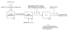
- a setup cycle correction method (a procedure of correcting and setting cycle data) according to this embodiment will be first explained with reference to FIG. 1 .
- This drawing is a flowchart showing a procedure of the setup cycle correction method.
- a user specifies a RATE set value of each domain (each core) in an electronic device (a step 10 ). Further, the RATE set value of each domain is adjusted in such a manner that the respective domains can be synchronized with each other (a step 11 ).
- a correction arithmetic operation is executed (a step 13 ) to readjust the RATE set values of the respective domains so that the respective domains can be synchronized with each other (a step 14 ).
- the readjusted RATE set values are set in a cycle setter 12 (which will be explained later) in a pattern generator 10 of a waveform generation apparatus (a semiconductor test apparatus) 1 (a step 15 ).
- a is the slowest cycle of a high-precision variable clock (a clock signal) output from a timing generator 40 .
- b is a cycle of a reference clock that is input to the timing generator 40 .
- c 1 is a phase of a cycle of cycle data with respect to an integral multiple of the reference clock cycle.
- T 1 is a cycle of spurious noise that occurs in the clock signal. Namely, this cycle is a phase fluctuation cycle.
- the reference clock cycle is divided by the phase, a quotient obtained by this division is multiplied by the cycle of the clock signal, and a product obtained by this multiplication is calculated as the cycle T 1 .
- e is a resolution concerning a setup cycle of the timing generator 40 .
- c 2 is a phase of a cycle of cycle data with respect to an integral multiple of the reference clock cycle.
- T 2 is a cycle of spurious noise that occurs in the clock signal. Namely, this cycle is a phase fluctuation cycle. A resolution of the timing generator is divided by the phase, a quotient obtained by this division is multiplied by the cycle of the clock signal, and a product obtained by this multiplication is calculated as the cycle T 2 .
- C 1 or C 2 that satisfies D in the following respective expressions is calculated.
- 1 /T 1 1/( A [ns] ⁇ B [ns]/ C 1[ns]))> D[ Hz] (Expression 3)
- 1 /T 2 1/( A [ns] ⁇ E [ns]/ C 2[ns])> D [Hz] (Expression 4)
- A is the slowest cycle of a high-precision variable clock (the clock signal).
- B is a cycle of a reference clock that is input to the timing generator 40 .
- C 1 is calculated as a value satisfying D, and the cycle data is corrected based on a value of m in this C 1 .
- D is a minimum value of a position where the spurious noise can be removed by the PLL 50 .
- E is a resolution concerning a setup cycle of the timing generator 40 .
- C 2 is calculated as a value satisfying D, and the cycle data is corrected based on a value of n in this C 2 .
- A is determined as the slowest cycle of the high-precision variable clock in order to assuredly enable removal of the spurious nose by the PLL 50 .
- the spurious noise can occur within a frequency range where removal by the PLL 50 is possible, thereby assuredly removing the spurious noise.
- cycle data is corrected based on C 1 and C 2 calculated based on Expressions 3 and 4.
- the spurious noise that occurs in the clock signal is allowed to occur at a position far from a carrier of this clock signal. Additionally, in Expressions 3 and 4, since C 1 or C 2 is calculated under the condition “>D”, the spurious noise occurs at a position where it can be removed by the PLL 50 . Therefore, the spurious noise can be assuredly removed, thereby realizing low jitters of the clock signal.
- a weight of an LSB (Less Significant Bit: a least significant bit when expressed in binary numbers) of the RATE set value is 2-28 ns
- a cycle of the reference clock is 4 ns
- a resolution concerning the setup cycle of the timing generator is 2 ⁇ 7 ns
- a position of the spurious noise that can be sufficiently removed by the PLL 50 is 40 kHz. It is to be noted that, when the position of the spurious noise is equal to or below 10 Hz, this position is not a target since it is too low.
- the RATE set value is determined as the following value.
- 1/RATE in this example is the following value.
- 1/RATE in this example has the following value.
- the RATE set value of each domain is readjusted.
- 1/RATE in this example has the following value.
- 1/T 1 and 1/T 2 have the following values, respectively.
- 1 /T 1 1/(13 ns ⁇ 4 ns/2 ⁇ 7 ns) ⁇ 150 kHz
- 1 /T 2 1/(13 ns ⁇ 2 ⁇ 7 ns/2 ⁇ 4 ns) ⁇ 601 kHz
- each of 1/T 1 and 1/T 2 is >40 kHz. Therefore, the produced spurious noise can be removed by the PLL 50 .
- the thus obtained RATE set value is set as cycle data by the cycle setter 12 in the pattern generator 10 .
- the setup cycle correction method of this embodiment since the cycle data is corrected in such a manner that a position where the spurious noise occurs become far from the carrier, this spurious noise can be assuredly removed by the PLL. Therefore, jitters of the high-precision variable clock can be reduced.
- Embodiments of a waveform generation apparatus and a semiconductor test apparatus that carry out the setup cycle correction method according to the present invention will now be explained with reference to FIGS. 4 to 7 .
- FIG. 4 is a block diagram showing a structure of a semiconductor test apparatus according to this embodiment
- FIG. 5 is a block diagram showing a structure of a pattern generator
- FIG. 6 is a block diagram showing a structure of a cycle generator
- FIG. 7 is a waveform chart showing a state of a signal in each portion in the pattern generator.
- the waveform generation apparatus is mounted in the semiconductor test apparatus to perform a multitime domain test.
- a waveform generation apparatus (a semiconductor test apparatus) 1 includes a pattern generator 10 , a timing generator 40 , and a PLL 50 .
- the pattern generator 10 includes a cycle generator 11 as shown in FIG. 5 .
- the cycle generator 11 outputs a pulse A 1 having a cycle that is m-fold (m is a positive integer) of a cycle T of a reference clock at a terminal 13 and a pulse A 2 having a cycle that is p-fold (p is a positive integer smaller than m) of the cycle T in accordance with setup cycle data.
- a setup cycle Ta is 8.5 T
- a cycle mT of the pulse A 1 alternately takes 8 T and 9 T
- a cycle pT of the pulse A 2 is 2 T.
- the cycle generator 11 outputs a micro cycle data RD indicative of a delay amount smaller than the cycle T in accordance with lower data of a weight of the cycle T or a smaller cycle of the setup cycle data and a generation state of the pulse A 1 .
- pulse A 1 and the micro cycle data RD output from the cycle generator 11 are generally represented as follows.
- a cycle of the pulse A 1 is obtained as follows.
- a sum total of a first setup cycle to an i+1th (i is an integer equal to or above 1) setup cycle of a timing pulse generated from this waveform generation apparatus 10 is divided by the cycle T to provide a value M 1 .
- a value obtained by subtracting an integer part of the value M 2 from an integer part of the value M 1 is multiplied by T, and a result is the cycle of the pulse A 1 .
- a decimal part of M 2 is the micro data RD.
- This cycle generator 11 is configured as shown in FIG. 6 . That is, the cycle setter 12 sets cycle data indicative of a cycle which should be generated. A bit number having a weight that is equal to or above the cycle T in the cycle data is determined as n 1 and a bit number having a weight that is less than T is determined as n 2 .
- a value obtained by subtracting T from the cycle which should be generated is set in the cycle setter 12 .
- the cycle which should be generated is 8.5 T, and “0011110” is set in accordance with this cycle as shown in FIG. 6 .
- An RS-FF 14 and a D-type FF 15 having n 2 bits are reset by using an initialization signal iNi from a terminal 16 in advance.
- the RS-FF14 When an activation signal START is supplied to a terminal 17 , the RS-FF14 is set, its Q output indicated by G 1 is changed to a high level, and gates 18 and 19 are opened based on the output G 1 . Further, the activation signal START is supplied to an OR gate 20 , a gate 21 is opened based on an output S 6 from this gate, and one of reference clocks CK is output as a pulse A 1 from a terminal 13 by the gate 21 .
- the output S 6 from the OR gate 20 is input to a load terminal LO of a down-counter 22 having n 1 bits, upper bits n 1 in the cycle setter 12 are preset in accordance with a falling edge of the reference clock CK in a state where the signal S 6 from the terminal LO is supplied, and 7 is output from the down-counter 22 as counting contents D 1 in this example. Then, the down-counter 22 counts down at the falling edge of each clock CK.
- the output S 6 from the OR gate 20 is also supplied to a differentiation circuit 23 , a counter 24 is cleared based on an output S 7 from the differentiation circuit 23 , and an output D 4 from this counter 24 becomes zero.
- the counter 24 multiplies a cycle of a pulse A 2 by p.
- p 2
- a signal S 8 having a width T is output from an AND gate 25 every time the counter 24 counts the two reference clocks CK.
- This signal S 8 is supplied to the gate 19 , and an output obtained by combining signals G 1 and S 8 and the clock CK is obtained as a pulse A 2 .
- n 2 in setup cycle data of the cycle setter 12 are supplied to an n 2 bit adder 26 , added to an output from the D-FF 15 , and an addition output is supplied to data terminals D 0 and D 1 of the D-FF 15 .
- n 2 2
- the adder 26 is a two-bit adder.
- a carry output C 1 from the adder 26 is inverted and supplied to a gate 27 , and supplied to a gate 28 without being inverted.
- the D-FF 15 is reset, and its output is 0. Therefore, the carry output C 1 is 0, and the gate 27 is opened.
- an output d 2 of upper bits in a two-bit output from the adder 26 is at the high level since lower two bits in the setup cycle data are 1 and 0 in this example.
- the D-FF 15 fetches the output from the adder 26 at a falling edge of an output S 5 from the gate 18 , and it produces an output as micro cycle data RD of the cycle generator 11 .
- the D-FF 15 and the adder 26 constitute an accumulation adding circuit.
- a zero detection circuit 29 produces an output S 1
- this output passes through the gate 27 and is further supplied to the gate 18 through an OR gate 30 as a signal S 2
- an output S 5 from the gate 18 is supplied to an OR gate 20 . Therefore, the gate 21 outputs one of the clocks CK which is 8 T separated as the pulse A 1 , the differentiation circuit 23 produces an output to clear the counter 24 , and setup cycle data is preset in the down-counter 22 .
- the output S 1 from the detection circuit 29 passes through the gate 28 when a count value of the down-counter 22 becomes zero next, thereby producing an output S 3 .
- This output is fetched into a D-FF 31 based on the next clock CK, and an output S 4 from the D-FF 31 is supplied to the gate 18 . Therefore, the pulse A 1 is produced from the gate 21 like the above, this pulse A 1 is 9 T from the previous pulse A 1 .
- the timing generator 40 has delay circuits 41 - 1 to 41 - n in units of reference clocks and a high-precision variable delay circuit 42 .
- a reference clock that is a reference for an output timing of a high-precision variable clock is input to the timing generator 40 .
- the PLL 50 includes a phase detector 51 , a loop filter 52 , a voltage controlled oscillator 53 , and an N divider 54 .
- the phase detector 51 outputs a phase difference between a reference frequency signal and an output signal from the N divider in the form of a voltage (or a current).
- the loop filter 52 determines a time constant of the PLL 50 .
- the voltage controlled oscillator 53 controls an output frequency by using a voltage.
- the N divider 54 divides a frequency of an output signal and supplies a divided frequency to an input side.
- the PLL 50 constitutes a feedback loop in which an output follows up a phase fluctuation in an input in such a manner that the output is returned to the phase detector 51 of the input and a phase difference between the input and the output is eliminated.
- the loop filter 52 is a low-pass filter, a phase fluctuation (spurious noise far from a carrier) having a faster frequency tends to be attenuated by the filter, and its output is hard to be followed up. Therefore, the spurious noise in the input is consequently removed.
- the waveform generation apparatus, the setup cycle correction method, and the semiconductor test apparatus according to the present invention have been explained above, the waveform generation apparatus, the setup cycle correction method, and the semiconductor test apparatus according to the present invention are not restricted to the foregoing embodiments, and various modifications can be carried out within the scope of the present invention.
- the present invention can be also applied to removal of noise that occurs with, e.g., a fixed frequency or cycle.
- its correction arithmetic operation can be formed as a program to be executed by an arithmetic operation device.
- this arithmetic operation device can be connected with the pattern generator in the waveform generation apparatus to input cycle data corrected by the arithmetic operation device to the pattern generator.
- the present invention is an invention concerning removal of spurious noise, it can be applied to an apparatus or a device that outputs a signal in which spurious noise occurs.
Landscapes
- Engineering & Computer Science (AREA)
- General Engineering & Computer Science (AREA)
- Physics & Mathematics (AREA)
- General Physics & Mathematics (AREA)
- Tests Of Electronic Circuits (AREA)
Abstract
Description
1/T1=1/(A×B/C1)>D
1/T2=1/(A×E/C2)>D
1/T1=1/(a[ns]×b[ns]/c1[ns])) (Expression 1)
1/T2=1/(a[ns]×e[ns]/c2[ns])) (Expression 2)
1/T1=1/(A[ns]×B[ns]/C1[ns]))>D[Hz] (Expression 3)
1/T2=1/(A[ns]×E[ns]/C2[ns])>D[Hz] (Expression 4)
1/T1=1/(13 ns×4 ns/2−23 ns)≈2.29 Hz
1/T2=1/(13 ns×2−7 ns/2−23 ns)≈1.17 Hz
1/T1=1/(13 ns×4 ns/2−7 ns)≈150 kHz
1/T2=1/(13 ns×2−7 ns/2−4 ns)≈601 kHz
Claims (8)
1/T1=1/(A×B/C1)>D
1/T2=1/(A×E/C2)>D
Applications Claiming Priority (2)
| Application Number | Priority Date | Filing Date | Title |
|---|---|---|---|
| JP2007141990A JP4856007B2 (en) | 2007-05-29 | 2007-05-29 | Waveform generator, set period correction method, and semiconductor test apparatus |
| JP2007-141990 | 2007-05-29 |
Publications (2)
| Publication Number | Publication Date |
|---|---|
| US20080297222A1 US20080297222A1 (en) | 2008-12-04 |
| US7768332B2 true US7768332B2 (en) | 2010-08-03 |
Family
ID=39942337
Family Applications (1)
| Application Number | Title | Priority Date | Filing Date |
|---|---|---|---|
| US11/811,514 Expired - Fee Related US7768332B2 (en) | 2007-05-29 | 2007-06-11 | Waveform generation apparatus, setup cycle correction method and semiconductor test apparatus |
Country Status (3)
| Country | Link |
|---|---|
| US (1) | US7768332B2 (en) |
| JP (1) | JP4856007B2 (en) |
| DE (1) | DE102008025770A1 (en) |
Cited By (1)
| Publication number | Priority date | Publication date | Assignee | Title |
|---|---|---|---|---|
| US20110204933A1 (en) * | 2008-09-12 | 2011-08-25 | Fujitsu Limited | Electric circuit and signal processing method |
Citations (4)
| Publication number | Priority date | Publication date | Assignee | Title |
|---|---|---|---|---|
| JPH0479545A (en) | 1990-07-19 | 1992-03-12 | Fujitsu Ltd | Subscriber communication information management system |
| US6255882B1 (en) * | 1998-04-28 | 2001-07-03 | Nec Corporation | Method and system of switching clock signal |
| EP1610137A1 (en) | 2004-06-24 | 2005-12-28 | Agilent Technologies, Inc. | Per-pin clock synthesis |
| WO2006058082A1 (en) | 2004-11-22 | 2006-06-01 | Teradyne, Inc. | Instrument with interface for synchronization in automatic test equipment |
Family Cites Families (2)
| Publication number | Priority date | Publication date | Assignee | Title |
|---|---|---|---|---|
| JP2001305196A (en) * | 2000-04-20 | 2001-10-31 | Advantest Corp | Control circuit |
| JP3514255B2 (en) * | 2002-01-10 | 2004-03-31 | 日本電気株式会社 | VCO circuit, PLL circuit, and information recording device |
-
2007
- 2007-05-29 JP JP2007141990A patent/JP4856007B2/en not_active Expired - Fee Related
- 2007-06-11 US US11/811,514 patent/US7768332B2/en not_active Expired - Fee Related
-
2008
- 2008-05-29 DE DE102008025770A patent/DE102008025770A1/en not_active Withdrawn
Patent Citations (4)
| Publication number | Priority date | Publication date | Assignee | Title |
|---|---|---|---|---|
| JPH0479545A (en) | 1990-07-19 | 1992-03-12 | Fujitsu Ltd | Subscriber communication information management system |
| US6255882B1 (en) * | 1998-04-28 | 2001-07-03 | Nec Corporation | Method and system of switching clock signal |
| EP1610137A1 (en) | 2004-06-24 | 2005-12-28 | Agilent Technologies, Inc. | Per-pin clock synthesis |
| WO2006058082A1 (en) | 2004-11-22 | 2006-06-01 | Teradyne, Inc. | Instrument with interface for synchronization in automatic test equipment |
Non-Patent Citations (1)
| Title |
|---|
| U. Tietze, Ch. Schenk "Halbleiter-Schaltungstechnik", Springer-Verlag, 1999, Seiten 1284-1295. |
Cited By (2)
| Publication number | Priority date | Publication date | Assignee | Title |
|---|---|---|---|---|
| US20110204933A1 (en) * | 2008-09-12 | 2011-08-25 | Fujitsu Limited | Electric circuit and signal processing method |
| US8415995B2 (en) * | 2008-09-12 | 2013-04-09 | Fujitsu Limited | Electric circuit and signal processing method |
Also Published As
| Publication number | Publication date |
|---|---|
| DE102008025770A1 (en) | 2008-12-11 |
| JP4856007B2 (en) | 2012-01-18 |
| JP2008298465A (en) | 2008-12-11 |
| US20080297222A1 (en) | 2008-12-04 |
Similar Documents
| Publication | Publication Date | Title |
|---|---|---|
| JP6664438B2 (en) | Apparatus and method for clock synchronization and frequency conversion | |
| JP4455757B2 (en) | Method and apparatus for adjusting the bandwidth of a phase locked loop | |
| KR101164477B1 (en) | Pll circuit, communication device, and loopback test method of communication device | |
| US10374617B2 (en) | Injection-locked digital bang-bang phase-locked loop with timing calibration | |
| US7800451B2 (en) | Frequency adjustment for clock generator | |
| CN103493377B (en) | Spur Suppression in Phase Locked Loops | |
| US7924071B2 (en) | Synchronization detection circuit, pulse width modulation circuit using the same, and synchronization detection method | |
| US20110273210A1 (en) | Low power digital phase lock loop circuit | |
| KR101277432B1 (en) | Clock data recovery device | |
| US7142823B1 (en) | Low jitter digital frequency synthesizer and control thereof | |
| US7382146B2 (en) | Semiconductor testing apparatus | |
| JP4886276B2 (en) | Clock data recovery device | |
| US8643412B2 (en) | Test apparatus, transmission apparatus, receiving apparatus, test method, transmission method and receiving method | |
| JP4298688B2 (en) | Clock generation circuit and clock generation method | |
| US7724093B2 (en) | Phase locked loop with two-step control | |
| US8392145B2 (en) | Timing generator | |
| JP4079733B2 (en) | Phase-locked loop circuit | |
| US7768332B2 (en) | Waveform generation apparatus, setup cycle correction method and semiconductor test apparatus | |
| JP2011234009A (en) | Clock and data recovery circuit | |
| KR101885033B1 (en) | Digital clock data recovery apparatus using delayed line phase frequency detection | |
| US9252785B2 (en) | Clock recovery for a data receiving unit | |
| KR101430796B1 (en) | Phase-frequency decector proving frequency multiplying, phase locked loop comprising the phase-frequency decector, and clock and data recovery circuit comprising the phase-frequency decector | |
| US10484027B2 (en) | Glitch free phase selection multiplexer enabling fractional feedback ratios in phase locked loops | |
| CN100481728C (en) | Clock data recovery device and method for low voltage differential signal | |
| CN120074468A (en) | Clock and data recovery circuitry |
Legal Events
| Date | Code | Title | Description |
|---|---|---|---|
| AS | Assignment |
Owner name: ADVANTEST CORPORATION, JAPAN Free format text: ASSIGNMENT OF ASSIGNORS INTEREST;ASSIGNOR:TAMURA, KENJI;REEL/FRAME:019806/0112 Effective date: 20070710 |
|
| FEPP | Fee payment procedure |
Free format text: PAYOR NUMBER ASSIGNED (ORIGINAL EVENT CODE: ASPN); ENTITY STATUS OF PATENT OWNER: LARGE ENTITY |
|
| REMI | Maintenance fee reminder mailed | ||
| LAPS | Lapse for failure to pay maintenance fees | ||
| STCH | Information on status: patent discontinuation |
Free format text: PATENT EXPIRED DUE TO NONPAYMENT OF MAINTENANCE FEES UNDER 37 CFR 1.362 |
|
| STCH | Information on status: patent discontinuation |
Free format text: PATENT EXPIRED DUE TO NONPAYMENT OF MAINTENANCE FEES UNDER 37 CFR 1.362 |
|
| FP | Lapsed due to failure to pay maintenance fee |
Effective date: 20140803 |