US7755446B2 - Waveguide and method for adjusting waveguide structure thereof - Google Patents
Waveguide and method for adjusting waveguide structure thereof Download PDFInfo
- Publication number
- US7755446B2 US7755446B2 US12/122,281 US12228108A US7755446B2 US 7755446 B2 US7755446 B2 US 7755446B2 US 12228108 A US12228108 A US 12228108A US 7755446 B2 US7755446 B2 US 7755446B2
- Authority
- US
- United States
- Prior art keywords
- waveguide
- connecting part
- buffer
- inches
- side length
- Prior art date
- Legal status (The legal status is an assumption and is not a legal conclusion. Google has not performed a legal analysis and makes no representation as to the accuracy of the status listed.)
- Expired - Fee Related, expires
Links
Images


Classifications
-
- H—ELECTRICITY
- H01—ELECTRIC ELEMENTS
- H01P—WAVEGUIDES; RESONATORS, LINES, OR OTHER DEVICES OF THE WAVEGUIDE TYPE
- H01P3/00—Waveguides; Transmission lines of the waveguide type
- H01P3/12—Hollow waveguides
-
- H—ELECTRICITY
- H01—ELECTRIC ELEMENTS
- H01P—WAVEGUIDES; RESONATORS, LINES, OR OTHER DEVICES OF THE WAVEGUIDE TYPE
- H01P1/00—Auxiliary devices
- H01P1/16—Auxiliary devices for mode selection, e.g. mode suppression or mode promotion; for mode conversion
- H01P1/161—Auxiliary devices for mode selection, e.g. mode suppression or mode promotion; for mode conversion sustaining two independent orthogonal modes, e.g. orthomode transducer
-
- H—ELECTRICITY
- H01—ELECTRIC ELEMENTS
- H01P—WAVEGUIDES; RESONATORS, LINES, OR OTHER DEVICES OF THE WAVEGUIDE TYPE
- H01P1/00—Auxiliary devices
- H01P1/165—Auxiliary devices for rotating the plane of polarisation
- H01P1/17—Auxiliary devices for rotating the plane of polarisation for producing a continuously rotating polarisation, e.g. circular polarisation
- H01P1/171—Auxiliary devices for rotating the plane of polarisation for producing a continuously rotating polarisation, e.g. circular polarisation using a corrugated or ridged waveguide section
Definitions
- the present invention relates to a waveguide, and more particularly, to a method for adjusting the structure of a waveguide to improve the quality of transmitting and receiving signals thereof.
- Waveguides are usually utilized in satellite communication to connect antenna and signal processing units, which execute signal processing of transmitting and receiving satellite signals.
- a circular polarized waveguide is composed of a splitter and a polarizer.
- the splitter divides transmitting satellite signals with the same phase into vertical and horizontal parts.
- the polarizer further shifts the vertical and horizontal satellite signals into satellite signals with phase difference of 90 degrees.
- the first embodiment of the present invention is a waveguide comprising a connecting part, a main chamber and a buffer.
- the buffer connects the connecting part and the main chamber.
- the side length of the junction between the connecting part and the buffer is smaller than that of the junction between the buffer and the main chamber.
- the second embodiment of the present invention is a method for adjusting the structure of a waveguide to improve the quality of its transmitting and receiving signals comprising the step of reducing a first side length of the junction between the connecting part and the buffer so that the first side length is shorter than a second side length of the junction between the main chamber and the buffer.
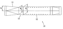
- FIG. 1A shows a part of the top view of a waveguide of the first embodiment of the present invention
- FIG. 1B shows a front view of a waveguide of the first embodiment of the present invention
- FIG. 1C shows a side view of a waveguide of the first embodiment of the present invention
- FIG. 2A shows a transmitting frequency response of the first embodiment of the present invention
- FIG. 2B shows another transmitting frequency response of the first embodiment of the present invention
- FIG. 2C shows yet another transmitting frequency response of the first embodiment of the present invention
- FIG. 3 shows a receiving frequency response of the first embodiment of the present invention.
- FIG. 4 shows a method for adjusting the structure of a waveguide to improve the quality of its transmitting and receiving signals of the second embodiment of the present invention.
- FIG. 1A shows a part of the top view of a waveguide 10 of the first embodiment of the present invention.
- FIG. 1B shows a front view of the waveguide 10 .
- FIG. 1C shows a side view of the waveguide 10 .
- the waveguide 10 comprises a connecting part 11 , a main chamber 12 and a buffer 13 as shown in FIGS. 1A & 1C .
- the connecting part 11 is a power splitter connecting to a signal processing unit to divide transmitting satellite signals having the same phase into vertical and horizontal parts.
- the main chamber 12 is a dual-band polarizer with a corrugated structure to shift the vertical and horizontal satellite signals into satellite signals with phase difference of 90 degrees being transmitted to an antenna.
- the buffer 13 connects the connecting part 11 and the main chamber 12 .
- the side length of the opening end of the connecting part 11 is W 1 .
- the side length of the junction between the connecting part 11 and the buffer 13 is W 2 .
- the side length of the junction between the buffer 13 and the main chamber 12 is W 3 .
- the length of the buffer 13 is L as shown in FIG. 1A .
- the waveguide 10 exhibits a high frequency transmitting band and a low frequency receiving band.
- W 2 is shortened in the first embodiment of the present invention to keep the spikes away from the transmitting frequency response.
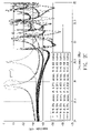
- FIG. 2A shows a transmitting frequency response (GHz) vs. magnitude (dB) response of the first embodiment of the present invention.
- GHz frequency response
- dB magnitude
- FIG. 2A shows a transmitting frequency response (GHz) vs. magnitude (dB) response of the first embodiment of the present invention.
- W 1 when W 1 is fixed at 0.374 inches and W 2 is fixed at 0.43 inches, as W 3 becomes shorter, (from 0.45 inches to 0.43 inches), fewer spikes are induced in the transmitting band of the waveguide 10 .
- the waveguide with the parameter W 3 as 0.43 inches has fewer spikes and lower magnitude in the transmitting band of 29.5 GHz to 30 GHz than the waveguide with the parameter W 3 as 0.45 inches.
- W 3 is between 0.425 and 0.435 inches.
- FIG. 2B shows another transmitting frequency response of the first (GHz) vs. magnitude (dB) response of the first embodiment of the present invention.
- W 1 when W 1 is fixed at 0.36 inches and W 3 is fixed at 0.43 inches, as W 2 becomes shorter (from 0.43 inches to 0.375 inches), the spikes induced become farther away from the transmitting band of the waveguide 10 .
- W 2 when W 2 is 0.43 inches, a spike is induced as marked by the encircled portion.
- W 2 becomes shorter (from 0.43 inches to 0.375 inches)
- the spikes induced become farther away from the transmitting band of 29.5 GHz to 30 GHz as marked by the arrow.
- the ratio of W 2 to W 1 is smaller than 1.2.
- FIG. 2C shows yet another transmitting frequency (GHz) vs. magnitude (dB) response of the first embodiment of the present invention.
- GHz transmitting frequency
- dB magnitude
- FIG. 2C shows yet another transmitting frequency (GHz) vs. magnitude (dB) response of the first embodiment of the present invention.
- W 1 when W 1 is fixed at 0.374 inches and W 3 is fixed at 0.43 inches, as W 2 becomes shorter (from 0.43 inches to 0.375 inches), the spikes induced become farther away from the transmitting band of the waveguide 10 .
- W 2 is 0.43 inches
- a spike is induced as marked by the encircled portion.
- W 2 becomes shorter (from 0.43 inches to 0.375 inches)
- the spikes induced become farther away from the transmitting band of 29.5 GHz to 30 GHz as marked by the arrow.
- the ratio of W 2 to W 1 is smaller than 1.07.
- W 1 is lengthened in the first embodiment of the present invention to reduce the proportion of the reflecting signals in the receiving band.
- FIG. 3 shows a receiving frequency (GHz) vs. magnitude (dB) response of the first embodiment of the present invention.
- GHz receiving frequency
- dB magnitude of the frequency response in the receiving band of 19.7 GHz to 20.2 GHz becomes higher.
- W 1 is between 0.35 and 0.375 inches.
- the waveguide 10 of the first embodiment of the present invention when applied in K band (18 GHz to 26.5 GHz) and Ka band (26.5 GHz to 40 GHz), can effectively improve the conventional waveguides and enhance their transmitting and receiving qualities.
- FIG. 4 shows a method for adjusting the structure of a waveguide to improve the quality of its transmitting and receiving signals of the second embodiment of the present invention.
- the waveguide includes a connecting part connected to a main chamber via a buffer.
- the connecting part is a power splitter and is connected to a signal processing unit.
- the main chamber is a polarizer and is connected to a signal processing unit.
- Step S 1 the side length of the junction between the connecting part and the buffer is reduced so that it is shorter than that of the junction between the main chamber and the buffer.
- Step S 2 the side length of the opening end of the connecting part is increased.
- the cross-junction of the waveguide of the present invention is not limited to a square shape as in the first embodiment, but can also include all kinds of shapes such as triangular shape, hexagonal shape, circular shape, and so on.
Landscapes
- Waveguide Switches, Polarizers, And Phase Shifters (AREA)
Abstract
Description
Claims (17)
Applications Claiming Priority (3)
| Application Number | Priority Date | Filing Date | Title |
|---|---|---|---|
| TW097100775A TWI351783B (en) | 2008-01-09 | 2008-01-09 | Waveguide and the structure adjusting method there |
| TW97100775A | 2008-01-09 | ||
| TW097100775 | 2008-01-09 |
Publications (2)
| Publication Number | Publication Date |
|---|---|
| US20090174506A1 US20090174506A1 (en) | 2009-07-09 |
| US7755446B2 true US7755446B2 (en) | 2010-07-13 |
Family
ID=40844110
Family Applications (1)
| Application Number | Title | Priority Date | Filing Date |
|---|---|---|---|
| US12/122,281 Expired - Fee Related US7755446B2 (en) | 2008-01-09 | 2008-05-16 | Waveguide and method for adjusting waveguide structure thereof |
Country Status (2)
| Country | Link |
|---|---|
| US (1) | US7755446B2 (en) |
| TW (1) | TWI351783B (en) |
Citations (4)
| Publication number | Priority date | Publication date | Assignee | Title |
|---|---|---|---|---|
| US2535251A (en) * | 1946-04-09 | 1950-12-26 | Alford Andrew | Rotatable wave guide joint |
| US4686491A (en) * | 1985-10-22 | 1987-08-11 | Chaparral Communications | Dual probe signal receiver |
| US5995057A (en) * | 1998-05-27 | 1999-11-30 | Trw Inc. | Dual mode horn reflector antenna |
| US6518853B1 (en) * | 2001-09-06 | 2003-02-11 | The Boeing Company | Wideband compact large step circular waveguide transition apparatus |
-
2008
- 2008-01-09 TW TW097100775A patent/TWI351783B/en not_active IP Right Cessation
- 2008-05-16 US US12/122,281 patent/US7755446B2/en not_active Expired - Fee Related
Patent Citations (4)
| Publication number | Priority date | Publication date | Assignee | Title |
|---|---|---|---|---|
| US2535251A (en) * | 1946-04-09 | 1950-12-26 | Alford Andrew | Rotatable wave guide joint |
| US4686491A (en) * | 1985-10-22 | 1987-08-11 | Chaparral Communications | Dual probe signal receiver |
| US5995057A (en) * | 1998-05-27 | 1999-11-30 | Trw Inc. | Dual mode horn reflector antenna |
| US6518853B1 (en) * | 2001-09-06 | 2003-02-11 | The Boeing Company | Wideband compact large step circular waveguide transition apparatus |
Also Published As
| Publication number | Publication date |
|---|---|
| TW200931710A (en) | 2009-07-16 |
| TWI351783B (en) | 2011-11-01 |
| US20090174506A1 (en) | 2009-07-09 |
Similar Documents
| Publication | Publication Date | Title |
|---|---|---|
| US8514134B2 (en) | MIMO antenna having parasitic elements | |
| WO2008033623A3 (en) | Stacked patch antennas | |
| US20080068274A1 (en) | Polarization transformation | |
| US8552914B2 (en) | Antenna and antenna assembly using same | |
| US9466880B2 (en) | Patch antenna having a patch fed with multiple signal | |
| JP5871647B2 (en) | Decoupling circuit | |
| CA2276338A1 (en) | Device for contactless transmission of electrical signals and/or energy | |
| WO2009031229A1 (en) | Antenna element | |
| US8049672B2 (en) | Ultra wideband antenna with band-notched characteristics | |
| WO2009108770A3 (en) | Antenna with dual band lumped element impedance matching | |
| US7573433B2 (en) | Dual-band antenna and mimo antenna using the same | |
| US6313714B1 (en) | Waveguide coupler | |
| WO2015107983A1 (en) | Antenna device | |
| JP2003531542A (en) | Dual band antenna | |
| US7755446B2 (en) | Waveguide and method for adjusting waveguide structure thereof | |
| JP2013251863A (en) | Impedance converter | |
| US20150180117A1 (en) | Inverted-f antenna provided with an isolation unit | |
| US20130314289A1 (en) | Phase shift device and method | |
| US20180248240A1 (en) | Compact antenna feeder with dual polarization | |
| WO2003015492A3 (en) | Isolating signal divider/combiner and method of combining signals of first and second frequencies | |
| US7474270B2 (en) | Electronic device with an internal antenna | |
| TWI466377B (en) | Multi-band printed antenna | |
| CN104900985B (en) | Antenna and wireless communication equipment | |
| US7535423B2 (en) | Multiple-band monopole coupling antenna | |
| JP5299749B2 (en) | Broadband power feeding circuit and slot antenna having the same |
Legal Events
| Date | Code | Title | Description |
|---|---|---|---|
| AS | Assignment |
Owner name: MICROELECTRONICS TECHNOLOGY INC., TAIWAN Free format text: ASSIGNMENT OF ASSIGNORS INTEREST;ASSIGNOR:LIN, CHIH JUNG;REEL/FRAME:020960/0682 Effective date: 20080512 |
|
| STCF | Information on status: patent grant |
Free format text: PATENTED CASE |
|
| FPAY | Fee payment |
Year of fee payment: 4 |
|
| MAFP | Maintenance fee payment |
Free format text: PAYMENT OF MAINTENANCE FEE, 8TH YEAR, LARGE ENTITY (ORIGINAL EVENT CODE: M1552) Year of fee payment: 8 |
|
| FEPP | Fee payment procedure |
Free format text: MAINTENANCE FEE REMINDER MAILED (ORIGINAL EVENT CODE: REM.); ENTITY STATUS OF PATENT OWNER: LARGE ENTITY |
|
| LAPS | Lapse for failure to pay maintenance fees |
Free format text: PATENT EXPIRED FOR FAILURE TO PAY MAINTENANCE FEES (ORIGINAL EVENT CODE: EXP.); ENTITY STATUS OF PATENT OWNER: LARGE ENTITY |
|
| STCH | Information on status: patent discontinuation |
Free format text: PATENT EXPIRED DUE TO NONPAYMENT OF MAINTENANCE FEES UNDER 37 CFR 1.362 |
|
| FP | Lapsed due to failure to pay maintenance fee |
Effective date: 20220713 |