US7732287B2 - Method of forming a body-tie - Google Patents
Method of forming a body-tie Download PDFInfo
- Publication number
- US7732287B2 US7732287B2 US11/415,703 US41570306A US7732287B2 US 7732287 B2 US7732287 B2 US 7732287B2 US 41570306 A US41570306 A US 41570306A US 7732287 B2 US7732287 B2 US 7732287B2
- Authority
- US
- United States
- Prior art keywords
- tie
- trench
- layer
- region
- silicon
- Prior art date
- Legal status (The legal status is an assumption and is not a legal conclusion. Google has not performed a legal analysis and makes no representation as to the accuracy of the status listed.)
- Expired - Lifetime
Links
Images


Classifications
-
- H—ELECTRICITY
- H10—SEMICONDUCTOR DEVICES; ELECTRIC SOLID-STATE DEVICES NOT OTHERWISE PROVIDED FOR
- H10D—INORGANIC ELECTRIC SEMICONDUCTOR DEVICES
- H10D30/00—Field-effect transistors [FET]
- H10D30/60—Insulated-gate field-effect transistors [IGFET]
- H10D30/67—Thin-film transistors [TFT]
- H10D30/6704—Thin-film transistors [TFT] having supplementary regions or layers in the thin films or in the insulated bulk substrates for controlling properties of the device
- H10D30/6708—Thin-film transistors [TFT] having supplementary regions or layers in the thin films or in the insulated bulk substrates for controlling properties of the device for preventing the kink effect or the snapback effect, e.g. discharging the minority carriers of the channel region for preventing bipolar effect
- H10D30/6711—Thin-film transistors [TFT] having supplementary regions or layers in the thin films or in the insulated bulk substrates for controlling properties of the device for preventing the kink effect or the snapback effect, e.g. discharging the minority carriers of the channel region for preventing bipolar effect by using electrodes contacting the supplementary regions or layers
-
- H—ELECTRICITY
- H10—SEMICONDUCTOR DEVICES; ELECTRIC SOLID-STATE DEVICES NOT OTHERWISE PROVIDED FOR
- H10D—INORGANIC ELECTRIC SEMICONDUCTOR DEVICES
- H10D30/00—Field-effect transistors [FET]
- H10D30/01—Manufacture or treatment
- H10D30/021—Manufacture or treatment of FETs having insulated gates [IGFET]
- H10D30/031—Manufacture or treatment of FETs having insulated gates [IGFET] of thin-film transistors [TFT]
- H10D30/0321—Manufacture or treatment of FETs having insulated gates [IGFET] of thin-film transistors [TFT] comprising silicon, e.g. amorphous silicon or polysilicon
- H10D30/0323—Manufacture or treatment of FETs having insulated gates [IGFET] of thin-film transistors [TFT] comprising silicon, e.g. amorphous silicon or polysilicon comprising monocrystalline silicon
Definitions
- the present invention relates generally to the field of Field Effect Transistors (FETs) fabricated in a Silicon-On-Insulator (SOI) substrate and more particularly to a method of forming a body-tie between a body-contact and a body of a FET.
- FETs Field Effect Transistors
- SOI Silicon-On-Insulator
- floating body effects are a result of having a body region that is electrically isolated from a bulk substrate.
- an applied bias is often supplied from a body-contact to the body.
- the body-contact receives an applied bias, which may be a ground or a positive or negative potential, it carries it to the body via a body tie.
- the body-tie is formed in device layer silicon and runs beneath an oxide.
- the body-tie allows the body region and the body-contact to be in remote locations in an SOI substrate.
- the body-tie may be exposed to a variety of processing steps during the fabrication of a FET.
- Implant steps may cause ions to penetrate the oxide layer and alter a body-tie's conductive properties.
- an SOI based process flow may need to include additional process steps to accommodate a body tie.
- an additional photo-resist mask may be needed to prevent implantation into the body-tie. This and other types of accommodation increase process complexity and decrease yield.
- a body-tie and a method of forming a body-tie are presented.
- the method includes forming a first trench in a device layer of an SOI substrate. Then, a second trench is formed in a portion of the first trench. The second trench stops in an insulating layer of the SOI substrate. A portion of the device layer that is located below the first trench and alongside the second trench serves as the body-tie.
- the device layer is silicon and the insulating layer is silicon dioxide and the first and second trenches together form a multi-tiered trench.
- the body-tie couples a FET body to a body-contact.
- the FET may be located in a silicon island that is next to the body tie.
- the silicon island and the body-tie may be viewed as a multi-tiered silicon island.
- An upper tier provides locations for source, drain, body, and body-contact regions.
- a lower tier which is buried beneath an isolation oxide, provides a body-tie location.
- the body-tie may be positioned so that it runs alongside the source region and not the drain region. To optimize area, the distance between at least two FETs may be reduced by sharing the body-tie. In one respect, the body-tie may be “self-aligned” with an edge of the first trench. Also, because the body-tie may be located below a thick oxide, a photo-resist mask may not be required to mask implants into the body-tie.
- FIG. 1A is a flow diagram of an STI scheme
- FIG. 1B is a flow diagram of a method of forming a body tie in the STI scheme of FIG. 1A ;
- FIG. 2 is a cross-section of an STI stack on an SOI substrate
- FIG. 3 is a cross-section of trenches formed in the SOI substrate
- FIG. 4 is a cross-section of a photoresist mask used to form body-ties and silicon islands
- FIG. 5 is a cross-section of implanted body-ties and islands
- FIG. 6 is a cross-section of a planarized oxide layer located above the body-ties of FIG. 5 ;
- FIG. 7 is a cross-section of a polysilicon layer located above the body-ties and islands of FIG. 6 ;
- FIG. 8 is a top view of the body-ties and islands of FIG. 7 ;
- FIG. 9 is a cross-section through the top view of FIG. 8 ;
- FIG. 10 is another cross-section cut through the top view of FIG. 8 ;
- FIG. 11 is yet another cross-section cut through the top view of FIG. 8 ;
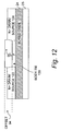
- FIG. 12 is a cross-section of two body regions sharing a body-tie.
- FIG. 1A is a flow diagram of a Shallow Trench Isolation (STI) scheme 10 .
- STI Shallow Trench Isolation
- CMOS complementary metal-oxide-semiconductor
- FIG. 1A presents a modification of an STI scheme in an SOI process to achieve a body-tie, a body-tie may be created using other types of isolation schemes or patterning and etching steps.
- STI scheme 10 begins at block 12 , where an STI stack is provided.
- FIG. 2 shows such an STI stack 14 .
- STI stack 14 includes a thin oxide layer 16 located on top of nitride layer 18 .
- the nitride layer 18 is located on top of a pad oxide layer 20 .
- the pad oxide layer 22 is located on top of a silicon device layer 22 .
- Device layer 22 is above a silicon dioxide insulating layer (buried oxide 24 ). Buried oxide 24 is on a bulk silicon substrate 25 .
- a photoresist mask defines a “hard-mask” pattern in STI stack 14 . After formation of the hard-mask, the photoresist may then be stripped.
- block 28 of STI scheme 10 includes method 30 .
- FIG. 1B is a flow diagram of method 30 .
- Method 30 begins after the STI hard-mask is formed.
- the SOI substrate will at least include a device layer located on top of an insulating layer, as shown at block 32 .
- method 30 at least two silicon etches are performed. This contrasts standard STI processing in SOI, where a silicon etch stops in the buried oxide 24 (or stops on the buried oxide 24 ). Instead, the silicon etch stops before the buried oxide 24 and first trenches are created, shown at block 32 .
- FIG. 3 is a cross-section showing this scenario.
- device layer 22 includes first trenches 36 , 38 , and 40 .
- Trench 38 isolates a P-type well 42 from an N-type well 44 .
- Trenches 36 and 40 in a likewise manner, may separate P-well 42 and N-well 44 from other devices located in device layer 22 .
- a thin portion of device layer 22 still exists in trenches 36 , 38 , and 40 .
- the silicon etch establishes a height 46 of a body-tie. The time of the silicon etch, therefore, is inversely proportional to the height of the body-tie.
- a second silicon etch creates a second set of trenches shown at block 48 of method 30 .
- these second trenches are not exclusively defined by the hard-mask. Instead, a photoresist mask defines them.
- photoresist mask 50 defines trenches 52 and 54 . Trenches 52 and 54 define the location of body-ties 56 and 58 .
- mask 50 establishes a width 55 of body-ties 56 and 58 via resist edges 60 and 62 . Although not shown, mask 50 also establishes a length of body-ties 56 and 58 .
- mask 50 may be open. For instance, mask 50 does not block the second silicon etch in trench 38 . Therefore, P-well 42 is completely separated from N-well 44 . However, in order to prevent shadowing in trench 38 , resist edges 64 and 66 are offset from the hard-mask. If edges 64 and 66 are not offset, the slope of the sidewalls of trench 38 may, as a result of the shadowing, decrease. Beyond edges 60 and 62 mask 50 is also open; thus, P-well 42 and N-well 44 are completely separated from other devices within device layer 22 .
- body-ties 56 and 58 and islands 66 and 68 are left behind.
- Island 66 includes P-well 42 and, upon completion of an SOI process flow, will also include an NFET.
- island 68 includes N-well 44 and will include a PFET.
- the combination of a body-tie and an island may be viewed as a multi-tiered island.
- body tie 56 and island 66 form a multi-tiered island 70 .
- body tie 58 and island 68 form a multi-tiered island 72 .
- Both multi-tiered islands 70 and 72 will house source, drain, body, and body-contact regions for a FET.
- body ties 56 and 58 provide a coupling between the body-contact and body regions of a FET.
- FIGS. 1A and 1B the STI etch process shown at block 28 of FIG. 1A is finished.
- the body-ties and trenches undergo implantation.
- FIG. 5 also shows this scenario.
- arrows 76 , 78 , 80 , and 82 point to implantation areas that may be implanted at block 74 .
- Arrows 76 for instance, point to a quad-type implant at the sidewalls of island 68 .
- Arrows 78 point to another quad-type implant at the sidewalls of island 70 .
- body ties 56 and 58 also receive implants, indicated by arrows 80 and 82 .
- the implants should be tailored so that body ties 56 and 58 have a concentration that is sufficiently high enough to prevent subsequent-opposite species type-implants from reverting either body-tie to an intrinsic or an opposite type doping. If such a consideration is not given, a diode may form between a body-tie and a gate and a body-tie and a body-contact. This will be described further with reference to FIG. 11 .
- an STI oxide is deposited at block 86 , and is planarized (chemically mechanically polished) at block 88 .
- FIG. 6 shows the outcome of the application of blocks 86 and 88 .
- an STI oxide 90 covers body-ties 56 and 58 and also provides electrical isolation between islands 66 and 68 . Additionally, STI oxide 90 electrically isolates islands 66 and 68 from other devices formed in the device layer.
- an SOI process continues to gate formation.
- the nitride layer 18 has been removed using a hot-phosphoric strip, for example.
- a polysilicon gate layer 92 which includes a thin gate oxide located below the polysilicon, is formed on top of islands 66 and 68 .
- the STI oxide 90 may be thinned or etched prior to the nitride layer 18 being removed. This thinning may determine an offset 94 of the STI oxide 90 above body-ties 56 and 58 .
- the offset 94 of STI oxide 90 protects body-ties 56 and 58 during subsequent implants. Implant protection will be further described with reference to FIG. 11 .
- FIG. 8 shows a top view of cutting planes through islands 66 and 68 and body ties 56 and 58 .
- FIGS. 9-11 respectively contain cross sections X-X′, Y-Y′, and Z-Z′.
- FIG. 8 also shows the locations of drain regions 96 and 98 , source regions 100 and 102 , and body-contact regions 104 and 106 of a respective NFET and PFET.
- cross-section X-X′ cuts through a body region 108 of island 66 and a body region 110 of island 68 .
- FIG. 9 also shows nitride spacers 112 and 114 located alongside gate layer 92 .
- cross section Y-Y′ which is perpendicular to cross section X-X′, cuts through island 66 .
- Drain 96 and source 100 show two implantation regions 116 and 118 .
- the first region 116 is a shallow, heavily doped region for providing an ohmic contact with silicided regions 120 and 122 . These silicided regions may be Ti-silicide or Co-silicide, for example.
- the first region has an average depth that is less than offset 94 (see FIG. 6 ).
- the second region 118 is a deeper, lightly doped region having an average depth that is greater than offset 94 .
- gate layer 92 should be sufficiently thick.
- gate layer 92 will not mask the implants that create regions 116 and 118 .
- a deeper implant bottoms out on the buried oxide 24 creating conduction paths under drain 96 and source 100 .
- shallow and deep implants may also create lightly and heavily P-type doped regions in the drain 98 and source 102 .
- cross section Z-Z′ cuts through source 100 and body tie 56 . Because body-tie 56 is located below STI oxide 90 , STI oxide 90 will mask the implant that creates region 116 . However, the deep implant that creates region 118 may still penetrate into body-tie 56 . By blocking the shallow implant, however, body tie 56 will remain of the same doping polarity as the body of the channel to provide the desired conductive path. However, as described above, if the body tie is not sufficiently doped at a previous step, a deep N-type implant may cause body-tie 56 to become intrinsic, or N-type. A P-N junction may be formed between body-contact 104 and body 108 .
- the STI oxide 90 may be tailored to a variety of thicknesses, proper offset 94 choice allows drains 96 and 98 and sources 100 and 102 to be implanted without requiring a photoresist mask or an extended gate layer to block heavy implants into the body-tie. Both of these attempts to block implants may lead to an increase in parasitic capacitance and/or device layout area. For instance, using a resist mask (in lieu of oxide layer 90 having offset 94 ) requires a significant increase in layout area due to the alignment and minimum line-width requirements associated with lithography steps. An extended gate layer, on the other hand, may increase parasitic capacitance by allowing an electric field to develop over the body tie. In essence, by eliminating the need for these types of masks, the implants into drains 96 and 98 and sources 100 and 102 may be truly self aligned.
- drains 96 and 98 may be walled in and a capacitance between the drains 96 and 98 and body-ties 56 and 58 will not develop. This type of alignment is demonstrated in FIG. 8 .
- FIG. 12 shows body tie 120 coupled to body regions 122 and 124 . Two separate FETs may include one of these body regions. Body-tie 120 may be manufactured in a similar fashion as method 32 .
- any number of FETs may share body-tie 120 . By sharing a body-tie, the distance between at least two FETs may be minimized.
- the second trench (formed at block 48 ) may not be formed within the first trench (formed at block 34 ). Instead, the first trench stops before the buried oxide and leaves the remaining portion of the device layer to be the body-tie. In such a scenario, a transistor may be surrounded by body-tie regions and may not require the electrical isolation that the second trench provides.
- the presented method has been described with reference to an STI scheme in an SOI process, it may, however, be carried out at other points of an SOI process.
- the presented body-tie may be particularly advantageous in radiation hardened circuits. Such circuits may use a body-contact along with the described body-tie to mitigate ion induced glitching and state changes. However, it is also contemplated that such a body-tie may also be used where appropriate in a non-radiation hardened circuit. It should be understood, therefore, that the illustrated examples are examples only and should not be taken as limiting the scope of the present invention.
- deposited is used generically to refer to the known growth, Chemical Vapor Deposition (CVD), plasma enhanced CVD, and other methods of fabricating dielectric or other semiconductor related films.
- CVD Chemical Vapor Deposition
- plasma enhanced CVD plasma enhanced CVD
Landscapes
- Element Separation (AREA)
- Thin Film Transistor (AREA)
- Semiconductor Memories (AREA)
Abstract
Description
Claims (14)
Priority Applications (4)
| Application Number | Priority Date | Filing Date | Title |
|---|---|---|---|
| US11/415,703 US7732287B2 (en) | 2006-05-02 | 2006-05-02 | Method of forming a body-tie |
| EP07749727.9A EP2013910B1 (en) | 2006-05-02 | 2007-02-01 | Method of forming a body-tie |
| PCT/US2007/002774 WO2007133306A2 (en) | 2006-05-02 | 2007-02-01 | Method of forming a body-tie |
| JP2009509550A JP5567832B2 (en) | 2006-05-02 | 2007-02-01 | How to form a body tie |
Applications Claiming Priority (1)
| Application Number | Priority Date | Filing Date | Title |
|---|---|---|---|
| US11/415,703 US7732287B2 (en) | 2006-05-02 | 2006-05-02 | Method of forming a body-tie |
Publications (2)
| Publication Number | Publication Date |
|---|---|
| US20070257317A1 US20070257317A1 (en) | 2007-11-08 |
| US7732287B2 true US7732287B2 (en) | 2010-06-08 |
Family
ID=38610678
Family Applications (1)
| Application Number | Title | Priority Date | Filing Date |
|---|---|---|---|
| US11/415,703 Expired - Lifetime US7732287B2 (en) | 2006-05-02 | 2006-05-02 | Method of forming a body-tie |
Country Status (4)
| Country | Link |
|---|---|
| US (1) | US7732287B2 (en) |
| EP (1) | EP2013910B1 (en) |
| JP (1) | JP5567832B2 (en) |
| WO (1) | WO2007133306A2 (en) |
Cited By (6)
| Publication number | Priority date | Publication date | Assignee | Title |
|---|---|---|---|---|
| US20110108943A1 (en) * | 2009-11-06 | 2011-05-12 | International Business Machines Corporation | Hybrid double box back gate silicon-on-insulator wafers with enhanced mobility channels |
| US20120112309A1 (en) * | 2009-01-12 | 2012-05-10 | International Business Machines Corporation | Low cost fabrication of double box back gate silicon-on-insulator wafers with subsequent self aligned shallow trench isolation |
| US8299544B2 (en) | 2011-01-04 | 2012-10-30 | International Business Machines Corporation | Field effect transistor having ohmic body contact(s), an integrated circuit structure incorporating stacked field effect transistors with such ohmic body contacts and associated methods |
| US8564069B1 (en) | 2012-08-21 | 2013-10-22 | International Business Machines Corporation | Field effect transistors with low body resistance and self-balanced body potential |
| US8975952B2 (en) | 2012-11-13 | 2015-03-10 | Honeywell International Inc. | CMOS logic circuit using passive internal body tie bias |
| US9773808B2 (en) | 2015-05-06 | 2017-09-26 | Honeywell International Inc. | Compact self-aligned implantation transistor edge resistor for SRAM SEU mitigation |
Families Citing this family (5)
| Publication number | Priority date | Publication date | Assignee | Title |
|---|---|---|---|---|
| US7679139B2 (en) * | 2007-09-11 | 2010-03-16 | Honeywell International Inc. | Non-planar silicon-on-insulator device that includes an “area-efficient” body tie |
| US7964897B2 (en) | 2008-07-22 | 2011-06-21 | Honeywell International Inc. | Direct contact to area efficient body tie process flow |
| US7939865B2 (en) * | 2009-01-22 | 2011-05-10 | Honeywell International Inc. | Metal semiconductor field effect transistor (MESFET) silicon-on-insulator structure having partial trench spacers |
| US8039837B2 (en) * | 2009-05-26 | 2011-10-18 | International Business Machines Corporation | In-line voltage contrast detection of PFET silicide encroachment |
| CN102254949B (en) * | 2011-08-01 | 2016-06-29 | 上海华虹宏力半导体制造有限公司 | Silicon-on-insulator mos transistor structure |
Citations (19)
| Publication number | Priority date | Publication date | Assignee | Title |
|---|---|---|---|---|
| US4489339A (en) | 1980-07-25 | 1984-12-18 | Tokyo Shibaura Denki Kabushiki Kaisha | SOS MOSFET With self-aligned channel contact |
| US4786955A (en) | 1987-02-24 | 1988-11-22 | General Electric Company | Semiconductor device with source and drain depth extenders and a method of making the same |
| US4809056A (en) | 1985-10-31 | 1989-02-28 | Fujitsu Limited | Semiconductor device having a silicon on insulator structure |
| US5145802A (en) | 1991-11-12 | 1992-09-08 | United Technologies Corporation | Method of making SOI circuit with buried connectors |
| US5767549A (en) | 1996-07-03 | 1998-06-16 | International Business Machines Corporation | SOI CMOS structure |
| GB2360874A (en) | 1999-10-25 | 2001-10-03 | Samsung Electronics Co Ltd | Eliminating floating body effects in SOI MOSFETS |
| WO2002025701A2 (en) | 2000-09-19 | 2002-03-28 | Motorola, Inc. | Body-tied silicon on insulator semiconductor device structure and method therefor |
| US20020123205A1 (en) * | 2000-02-17 | 2002-09-05 | Toshiaki Iwamatsu | Semiconductor device and method of manufacturing the same |
| US20030020117A1 (en) | 2001-07-28 | 2003-01-30 | Samsung Electronics Co., Ltd. | Silicon on insulator device having trench isolation layer and method for manufacturing the same |
| US6521959B2 (en) | 1999-10-25 | 2003-02-18 | Samsung Electronics Co., Ltd. | SOI semiconductor integrated circuit for eliminating floating body effects in SOI MOSFETs and method of fabricating the same |
| US6537861B1 (en) | 1998-08-29 | 2003-03-25 | International Business Machines Corporation | SOI transistor with body contact and method of forming same |
| US6638799B2 (en) * | 2001-02-07 | 2003-10-28 | Matsushita Electric Industrial Co., Ltd. | Method for manufacturing a semiconductor device having a silicon on insulator substrate |
| US6724048B2 (en) | 2001-12-19 | 2004-04-20 | Motorola, Inc. | Body-tied silicon on insulator semiconductor device and method therefor |
| US20040129975A1 (en) | 2002-12-06 | 2004-07-08 | Nec Corporation | Semiconductor device and method for manufacturing the same |
| US6864152B1 (en) | 2003-05-20 | 2005-03-08 | Lsi Logic Corporation | Fabrication of trenches with multiple depths on the same substrate |
| US6953809B2 (en) | 1997-08-07 | 2005-10-11 | Zeneca Limited | Monocyte chemoattractant protein-1 inhibitor compounds |
| US6960810B2 (en) | 2002-05-30 | 2005-11-01 | Honeywell International Inc. | Self-aligned body tie for a partially depleted SOI device structure |
| US20050269637A1 (en) | 2004-06-03 | 2005-12-08 | Renesas Technology Corp. | Semiconductor device |
| US7179717B2 (en) * | 2005-05-25 | 2007-02-20 | Micron Technology, Inc. | Methods of forming integrated circuit devices |
Family Cites Families (3)
| Publication number | Priority date | Publication date | Assignee | Title |
|---|---|---|---|---|
| JP2002261292A (en) * | 2000-12-26 | 2002-09-13 | Toshiba Corp | Semiconductor device and manufacturing method thereof |
| JP2002246600A (en) * | 2001-02-13 | 2002-08-30 | Mitsubishi Electric Corp | Semiconductor device and manufacturing method thereof |
| JP2004072063A (en) * | 2002-06-10 | 2004-03-04 | Nec Electronics Corp | Semiconductor device and manufacturing method thereof |
-
2006
- 2006-05-02 US US11/415,703 patent/US7732287B2/en not_active Expired - Lifetime
-
2007
- 2007-02-01 WO PCT/US2007/002774 patent/WO2007133306A2/en not_active Ceased
- 2007-02-01 EP EP07749727.9A patent/EP2013910B1/en not_active Ceased
- 2007-02-01 JP JP2009509550A patent/JP5567832B2/en active Active
Patent Citations (19)
| Publication number | Priority date | Publication date | Assignee | Title |
|---|---|---|---|---|
| US4489339A (en) | 1980-07-25 | 1984-12-18 | Tokyo Shibaura Denki Kabushiki Kaisha | SOS MOSFET With self-aligned channel contact |
| US4809056A (en) | 1985-10-31 | 1989-02-28 | Fujitsu Limited | Semiconductor device having a silicon on insulator structure |
| US4786955A (en) | 1987-02-24 | 1988-11-22 | General Electric Company | Semiconductor device with source and drain depth extenders and a method of making the same |
| US5145802A (en) | 1991-11-12 | 1992-09-08 | United Technologies Corporation | Method of making SOI circuit with buried connectors |
| US5767549A (en) | 1996-07-03 | 1998-06-16 | International Business Machines Corporation | SOI CMOS structure |
| US6953809B2 (en) | 1997-08-07 | 2005-10-11 | Zeneca Limited | Monocyte chemoattractant protein-1 inhibitor compounds |
| US6537861B1 (en) | 1998-08-29 | 2003-03-25 | International Business Machines Corporation | SOI transistor with body contact and method of forming same |
| GB2360874A (en) | 1999-10-25 | 2001-10-03 | Samsung Electronics Co Ltd | Eliminating floating body effects in SOI MOSFETS |
| US6521959B2 (en) | 1999-10-25 | 2003-02-18 | Samsung Electronics Co., Ltd. | SOI semiconductor integrated circuit for eliminating floating body effects in SOI MOSFETs and method of fabricating the same |
| US20020123205A1 (en) * | 2000-02-17 | 2002-09-05 | Toshiaki Iwamatsu | Semiconductor device and method of manufacturing the same |
| WO2002025701A2 (en) | 2000-09-19 | 2002-03-28 | Motorola, Inc. | Body-tied silicon on insulator semiconductor device structure and method therefor |
| US6638799B2 (en) * | 2001-02-07 | 2003-10-28 | Matsushita Electric Industrial Co., Ltd. | Method for manufacturing a semiconductor device having a silicon on insulator substrate |
| US20030020117A1 (en) | 2001-07-28 | 2003-01-30 | Samsung Electronics Co., Ltd. | Silicon on insulator device having trench isolation layer and method for manufacturing the same |
| US6724048B2 (en) | 2001-12-19 | 2004-04-20 | Motorola, Inc. | Body-tied silicon on insulator semiconductor device and method therefor |
| US6960810B2 (en) | 2002-05-30 | 2005-11-01 | Honeywell International Inc. | Self-aligned body tie for a partially depleted SOI device structure |
| US20040129975A1 (en) | 2002-12-06 | 2004-07-08 | Nec Corporation | Semiconductor device and method for manufacturing the same |
| US6864152B1 (en) | 2003-05-20 | 2005-03-08 | Lsi Logic Corporation | Fabrication of trenches with multiple depths on the same substrate |
| US20050269637A1 (en) | 2004-06-03 | 2005-12-08 | Renesas Technology Corp. | Semiconductor device |
| US7179717B2 (en) * | 2005-05-25 | 2007-02-20 | Micron Technology, Inc. | Methods of forming integrated circuit devices |
Non-Patent Citations (4)
| Title |
|---|
| International Preliminary Report on Patentability for PCT/US2007/002774, 9 pgs., dated Nov. 13, 2008. |
| International Search Report for PCT/US2007/002774 dated Nov. 6, 2007. |
| Min, B.W., et al., "Partial Trench Isolated Body-Tied (PTIBT) Structure for SOI Applications," Oct. 2001, IEEE International SOI Conference, pp. 71-72. |
| Wolf, Silicon Processing for the VLSI Era, vol. 2: Process Integration, 1990 by Lattice Press, pp. 143-147. * |
Cited By (8)
| Publication number | Priority date | Publication date | Assignee | Title |
|---|---|---|---|---|
| US20120112309A1 (en) * | 2009-01-12 | 2012-05-10 | International Business Machines Corporation | Low cost fabrication of double box back gate silicon-on-insulator wafers with subsequent self aligned shallow trench isolation |
| US8877606B2 (en) * | 2009-01-12 | 2014-11-04 | International Business Machines Corporation | Low cost fabrication of double box back gate silicon-on-insulator wafers with subsequent self aligned shallow trench isolation |
| US20110108943A1 (en) * | 2009-11-06 | 2011-05-12 | International Business Machines Corporation | Hybrid double box back gate silicon-on-insulator wafers with enhanced mobility channels |
| US8587063B2 (en) | 2009-11-06 | 2013-11-19 | International Business Machines Corporation | Hybrid double box back gate silicon-on-insulator wafers with enhanced mobility channels |
| US8299544B2 (en) | 2011-01-04 | 2012-10-30 | International Business Machines Corporation | Field effect transistor having ohmic body contact(s), an integrated circuit structure incorporating stacked field effect transistors with such ohmic body contacts and associated methods |
| US8564069B1 (en) | 2012-08-21 | 2013-10-22 | International Business Machines Corporation | Field effect transistors with low body resistance and self-balanced body potential |
| US8975952B2 (en) | 2012-11-13 | 2015-03-10 | Honeywell International Inc. | CMOS logic circuit using passive internal body tie bias |
| US9773808B2 (en) | 2015-05-06 | 2017-09-26 | Honeywell International Inc. | Compact self-aligned implantation transistor edge resistor for SRAM SEU mitigation |
Also Published As
| Publication number | Publication date |
|---|---|
| EP2013910B1 (en) | 2019-06-12 |
| WO2007133306A3 (en) | 2008-01-24 |
| US20070257317A1 (en) | 2007-11-08 |
| WO2007133306A2 (en) | 2007-11-22 |
| EP2013910A2 (en) | 2009-01-14 |
| JP2009535844A (en) | 2009-10-01 |
| JP5567832B2 (en) | 2014-08-06 |
Similar Documents
| Publication | Publication Date | Title |
|---|---|---|
| EP2013910B1 (en) | Method of forming a body-tie | |
| US7192816B2 (en) | Self-aligned body tie for a partially depleted SOI device structure | |
| KR100243715B1 (en) | CMOS structure with FET in isolated well with depletion unit and method | |
| US6153455A (en) | Method of fabricating ultra shallow junction CMOS transistors with nitride disposable spacer | |
| US7008836B2 (en) | Method to provide a triple well in an epitaxially based CMOS or BiCMOS process | |
| US6855581B2 (en) | Method for fabricating a high-voltage high-power integrated circuit device | |
| US5315144A (en) | Reduction of bipolar gain and improvement in snap-back sustaining voltage in SOI field effect transistor | |
| US11374124B2 (en) | Protection of drain extended transistor field oxide | |
| US5943576A (en) | Angled implant to build MOS transistors in contact holes | |
| US7557393B2 (en) | JFET with built in back gate in either SOI or bulk silicon | |
| US20120267724A1 (en) | Mos semiconductor device and methods for its fabrication | |
| US5612240A (en) | Method for making electrical connections to self-aligned contacts that extends beyond the photo-lithographic resolution limit | |
| US7419874B2 (en) | Method of manufacturing semiconductor device with capacitor and transistor | |
| US6991983B2 (en) | Method of manufacturing high voltage transistor in flash memory device | |
| US7646057B2 (en) | Gate structure with first S/D aside the first gate in a trench and the second gate with second S/D in the epitaxial below sides of the second gate on the first gate | |
| US6566696B1 (en) | Self-aligned VT implant | |
| US6448121B1 (en) | High threshold PMOS transistor in a surface-channel process | |
| US8962410B2 (en) | Transistors with different threshold voltages | |
| US7176095B1 (en) | Bi-modal halo implantation | |
| US20250221053A1 (en) | Integrated circuit device with zener diode with reduced leakage and/or increased breakdown voltage | |
| KR100305641B1 (en) | Semiconductor element formed on SOH substrate and its manufacturing method | |
| US20090096037A1 (en) | Semiconductor device having recessed field region and fabrication method thereof | |
| KR100609532B1 (en) | Manufacturing Method of SOI Semiconductor Device |
Legal Events
| Date | Code | Title | Description |
|---|---|---|---|
| AS | Assignment |
Owner name: HONEYWELL INTERNATIONAL INC., NEW JERSEY Free format text: ASSIGNMENT OF ASSIGNORS INTEREST;ASSIGNORS:FECHNER, PAUL S.;SHAW, GORDON A.;VOGT, ERIC E.;REEL/FRAME:017853/0468;SIGNING DATES FROM 20060428 TO 20060501 Owner name: HONEYWELL INTERNATIONAL INC.,NEW JERSEY Free format text: ASSIGNMENT OF ASSIGNORS INTEREST;ASSIGNORS:FECHNER, PAUL S.;SHAW, GORDON A.;VOGT, ERIC E.;SIGNING DATES FROM 20060428 TO 20060501;REEL/FRAME:017853/0468 |
|
| STCF | Information on status: patent grant |
Free format text: PATENTED CASE |
|
| AS | Assignment |
Owner name: UNITED STATES GOVERNMENT; DEFENSE THREAT REDUCTION Free format text: CONFIRMATORY LICENSE;ASSIGNOR:HONEYWELL INTERNATIONAL INC.;REEL/FRAME:025709/0368 Effective date: 20110126 |
|
| CC | Certificate of correction | ||
| FPAY | Fee payment |
Year of fee payment: 4 |
|
| MAFP | Maintenance fee payment |
Free format text: PAYMENT OF MAINTENANCE FEE, 8TH YEAR, LARGE ENTITY (ORIGINAL EVENT CODE: M1552) Year of fee payment: 8 |
|
| FEPP | Fee payment procedure |
Free format text: MAINTENANCE FEE REMINDER MAILED (ORIGINAL EVENT CODE: REM.); ENTITY STATUS OF PATENT OWNER: LARGE ENTITY |
|
| FEPP | Fee payment procedure |
Free format text: 11.5 YR SURCHARGE- LATE PMT W/IN 6 MO, LARGE ENTITY (ORIGINAL EVENT CODE: M1556); ENTITY STATUS OF PATENT OWNER: LARGE ENTITY |
|
| MAFP | Maintenance fee payment |
Free format text: PAYMENT OF MAINTENANCE FEE, 12TH YEAR, LARGE ENTITY (ORIGINAL EVENT CODE: M1553); ENTITY STATUS OF PATENT OWNER: LARGE ENTITY Year of fee payment: 12 |