US7724622B2 - Recording device capable of determining the media type based on detecting the capacitance of pair electrodes - Google Patents
Recording device capable of determining the media type based on detecting the capacitance of pair electrodes Download PDFInfo
- Publication number
- US7724622B2 US7724622B2 US11/764,810 US76481007A US7724622B2 US 7724622 B2 US7724622 B2 US 7724622B2 US 76481007 A US76481007 A US 76481007A US 7724622 B2 US7724622 B2 US 7724622B2
- Authority
- US
- United States
- Prior art keywords
- recording medium
- tray
- threshold voltage
- electrodes
- recording
- Prior art date
- Legal status (The legal status is an assumption and is not a legal conclusion. Google has not performed a legal analysis and makes no representation as to the accuracy of the status listed.)
- Expired - Fee Related, expires
Links
Images


Classifications
-
- G—PHYSICS
- G11—INFORMATION STORAGE
- G11B—INFORMATION STORAGE BASED ON RELATIVE MOVEMENT BETWEEN RECORD CARRIER AND TRANSDUCER
- G11B17/00—Guiding record carriers not specifically of filamentary or web form, or of supports therefor
- G11B17/02—Details
- G11B17/04—Feeding or guiding single record carrier to or from transducer unit
- G11B17/05—Feeding or guiding single record carrier to or from transducer unit specially adapted for discs not contained within cartridges
- G11B17/051—Direct insertion, i.e. without external loading means
- G11B17/0515—Direct insertion, i.e. without external loading means adapted for discs of different sizes
Definitions
- the present invention relates to a device and method for detecting a recording medium.
- Japanese Laid-Open Patent Publication No. 2003-346336 describes a detection device that emits laser light toward an optical disc, detects the reflected light, and compares a signal level of the reflected light with a predetermined threshold to determine the media type.
- Japanese Laid-Open Patent Publication No. 2005-302083 describes an optical disc recorder that emits laser light toward the recording surface of an optical disc to recognize the media type based on variations in the signal level of the reflected light, the intensity of the signal level, and fluctuation tendencies in the signal level relative to the intensity of the emitted laser light.
- the prior art devices described in the above publications detect the media type using reflected laser light. This results in complicated processing. Further, the media type may not be accurately detected when the surface of the optical disc includes a scratch or a smear.
- the prior art devices also cannot detect the media type unless an optical disc is loaded into a drive device. In other words, the optical device cannot be detected when a media tray projects from the drive device. Thus, there is no way to determine whether or not the optical disc is properly set on the media tray before retraction of the media tray into the drive device.
- FIG. 1 is a schematic diagram showing a media detection device according to a first embodiment of the present invention
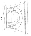
- FIG. 2 is a perspective view showing two electrodes of the detection device of FIG. 1 ;
- FIG. 3A is a schematic cross-sectional view of a CD
- FIG. 3B is a schematic cross-sectional view of a DVD
- FIG. 3C is a schematic cross-sectional view of a BD
- FIG. 4 is a graph showing detections of an electric field sensor shown in FIG. 1 indicating the media type
- FIG. 5A is a cross-sectional diagram showing a recording medium set on a tray in a proper state
- FIG. 5B is a cross-sectional diagram showing a recording medium set on a tray in an inclined state
- FIG. 5C is a cross-sectional diagram showing a recording medium set on a tray in a state of non-contact with the electrodes;
- FIG. 6 is a schematic diagram showing a recording medium in states displaced from the tray.
- FIG. 7 is a graph showing detections of the electric field sensor of FIG. 1 indicating the medium position.
- the present invention provides a device and method enabling easy detection of a recording medium set on a media tray.
- One aspect of the present invention is a device for detecting a recording medium placed on a tray.
- the device includes at least two electrodes arranged on the tray.
- An electric field sensor is connected to the electrodes to detect capacitance with respect to distance between the electrodes relative to the recording medium placed on the tray.
- Another aspect of the invention is a method for recording media type recognition of a recording medium placed on a tray.
- the detection device includes at least two electrodes arranged on the tray and an electric field sensor connected to the electrodes.
- the method includes detecting capacitance in accordance with the distance between the electrodes relative to the recording medium placed on the tray with the electric field sensor, and recognizing the recording media type based on the capacitance detected by the electric field sensor.
- a further aspect of the present invention is a method for detecting where a recording medium placed on a tray is located with use of a detection device.
- the detection device includes at least two electrodes arranged on the tray and an electric field sensor connected to the electrodes.
- the method includes detecting capacitance in accordance with the distance between the electrodes relative to the recording medium placed on the tray with the electric field sensor, and determining where the recording medium is located on the tray based on the capacitance detected by the electric field sensor.
- a media detection device 10 according to a first embodiment of the present invention will now be discussed with reference to FIGS. 1 to 7 .
- FIG. 1 is a schematic diagram showing the entire structure of the media detection device 10 .
- the media detection device 10 includes two electrodes 30 and 32 , an electric field sensor 40 connected to the electrodes 30 and 32 , and a control circuit 50 connected to the electric field sensor 40 .
- the electric field sensor 40 and the control circuit 50 are arranged in a drive device 20 ( FIG. 2 ) into which a recording medium 100 is loaded.
- the two electrodes 30 and 32 are arranged on a media tray 22 , which is projectable from and retractable into the drive device 20 .
- the media tray 22 is configured so that the recording medium 100 can be placed on the two electrodes 30 and 32 .
- FIG. 1 schematically shows the cross-sectional shapes of the recording medium 100 and the media tray 22 .
- the recording medium 100 is an optical disc, such as a compact disc (hereafter referred to as a CD), a digital versatile disc (hereafter referred to as a DVD), or a Blu-ray DiscTM (hereafter referred to as a BD). More specifically, a CD may be an optical disc that is in compliance with any of a plurality of CD standards, such as a CD-ROM (read only memory), a CD-R (recordable), and a CD-RW (rewritable).
- CD-ROM read only memory
- CD-R recordable
- CD-RW rewritable
- a DVD may be an optical disc that is in compliance with any of a plurality of DVD standards, such as a DVD-ROM, a DVD-R, a dual layer DVD-R, a DVD-RW, a DVD-RAM (random access memory), an HDDVDTM-R (high-definition digital versatile disc recordable).
- a BD may be an optical disc that is in compliance with any of a plurality of BD standards, such as a BD-R and a BR-RW.
- the drive device 20 which is applicable to the CD standard, the DVD standard, and the BD standard, emits laser light from an optical pickup (not shown) in accordance with the standard of the recording medium 100 to control the writing and reading of data.
- the media tray 22 includes a first seat surface 24 on which a recording medium having a diameter of 12 cm is receivable and a second seat surface 26 on which a recording medium having a diameter of 8 cm is receivable.
- the second seat surface 26 is located at the inner side of the first seat surface 24 and is lower than the first seat surface 24 .
- a cutout portion 28 is defined in the center of the media tray 22 extending through the first and second seat surfaces 24 and 26 .
- the two electrodes 30 and 32 are fixed to the first and second seat surfaces 24 and 26 of the media tray 22 . Since the electrodes 30 and 32 have identical structures, the structure of only the electrode 30 will be described.
- the electrode 30 includes a first electrode portion 30 a fixed to the first seat surface 24 , a second electrode portion 30 b fixed to the second seat surface 26 , and a connection portion 30 c connecting the first and second electrode portions 30 a and 30 b .
- the first electrode portion 30 a is arcuate, and the second electrode portion 30 b is semicircular. However, the first and second electrode portions 30 a and 30 b do not necessarily have to be shaped as shown in FIG. 2 .
- the electrode portions 30 a and 30 b are formed so as to provide a large area of contact with the corresponding recording media.
- the electrode 32 is formed identically to the electrode 30 . More specifically, the electrode 32 includes a first electrode portion 32 a , a second electrode portion 32 b , and a connection portion 32 c located between the first and second electrode portions 32 a and 32 b .
- the electrodes 30 and 32 have the same area.
- the recording medium 100 includes a protective layer (resin layer) 102 , a recording layer 104 having a metal film, and a substrate 106 having a printing surface. Data is recorded to the recording layer 104 .
- the recording medium 100 is set on the media tray 22 with the protective layer 102 facing downwards. When the recording medium 100 is properly set at the appropriate position on the media tray 22 , the electrodes 30 and 32 come into contact with the protective layer 102 of the recording medium 100 .
- the control circuit 50 controls the electric field sensor 40 .
- the electric field sensor 40 transmits a predetermined sine wave signal to the electrodes 30 and 32 in response to a control signal SC, which is transmitted from the control circuit 50 .
- the electric field sensor 40 Based on the fluctuation amount of the amplitude and phase of the sine wave signal at the electrodes 30 and 32 , the electric field sensor 40 detects capacitance C, which is in accordance with the distance d from the recording layer 104 of the recording media 100 to the electrodes 30 and 32 .
- the electric field sensor 40 generates a sense voltage Vsense, which indicates the detected capacitance D, and transmits the sense voltage Vsense to the control circuit 50 .
- k represents the dielectric constant of the substance between the electrodes 30 and 32 .
- k corresponds to the dielectric constant of the protective layer 102 .
- ⁇ 0 represents the vacuum dielectric constant (8.85 ⁇ 10 12 F/m)
- A represents the area (m 2 ) of each of the electrodes 30 and 32
- D represents the distance (m) between the electrodes 30 and 32 .
- the control circuit 50 recognizes the media type of the recording medium 100 based on the sensor voltage Vsense measured by the electric field sensor 40 . For example, when the media tray 22 is projected from the drive device 20 , the electric field sensor 40 starts a sensing operation in response to a command from the control circuit 50 . The electric field sensor 40 detects the capacitance C, which corresponds to the distance d of the electrodes 30 and 32 from the recording layer 104 of the recording media 100 on the media tray 22 . Then, the electric field sensor 40 transmits the sense voltage Vsense, which indicates the detection, to the control circuit 50 .
- FIGS. 3A , 3 B, and 3 C are schematic cross-sectional views showing three recording media of different media types.
- FIG. 3A shows a CD 110
- FIG. 3B shows a DVD 120
- FIG. 3C shows a ED 130 .
- the distance d 1 from the surface of a protective layer 112 to a recording layer 114 between the protective layer 112 and a substrate 116 is approximately 1.2 mm.
- the distance d 2 from the surface of a protective layer 122 to a recording layer 124 between the protective layer 122 and a substrate 126 is approximately 0.6 mm.
- the distance d 3 from the surface of a protective layer 132 to a recording layer 134 between the protective layer 132 and a substrate 136 is approximately 0.1 mm.
- the distance between the electrodes 30 and 32 relative to the recording layer of the recording medium i.e., the distance D in equation 1
- the capacitance C detected by the electric field sensor 40 differs between different media types.
- the capacitances detected for the CD 110 , the DVD 120 , and the BD 130 are respectively represented by C 1 , C 2 , and C 3
- the relationship of C 1 ⁇ C 2 ⁇ C 3 is satisfied.
- the CD 110 , the DVD 120 , and the BD 130 respectively have sense voltages V 1 , V 2 , and V 3 that satisfy the relationship of V 1 >V 2 >V 3 .
- the control circuit 50 compares the sense voltage Vsense measured by the electric field sensor 40 with a first threshold voltage Vth 1 and a second threshold voltage Vth 2 .
- the first threshold voltage Vth 1 is set at a value enabling the CD 110 to be distinguished from the DVD 120 .
- the second threshold voltage Vth 2 is set at a value enabling the DVD 120 to be distinguished from the BD 130 . Accordingly, the first threshold voltage Vth 1 is higher than the second threshold voltage Vth 2 .
- the control circuit 50 determines that the recording medium 100 is the CD 110 .
- the control circuit 50 determines that the recording medium 100 is the DVD 120 .
- the control circuit 50 determines that the recording medium 100 is the BD 130 .
- FIG. 4 is a graph showing detections (measurement values) of the electric field sensor 40 indicating the media type.
- the graph shows the measurement values of the sense voltage Vsense for three CD standards (CD-ROM, CD-R, and CD-RW), six DVD standards (DVD-ROM, DVD-R, dual layer DVD-R, DVD-RW, DVD-RAM, and HDDVD-R), and one BD standard (BD-R).
- the sense voltage Vsense is measured in a range of approximately 2.60 V to 2.70 V.
- the sense voltage Vsense is measured in a range of approximately 2.30 V to 2.50 V.
- the sense voltage Vsense is measured in the vicinity of approximately 2.00 V.
- the first threshold voltage Vth 1 is set at, for example, 2.55 V
- the second threshold value Vth 2 is set at, for example, 2.25 V in the preferred embodiment. Accordingly, when the sense voltage Vsense is greater than 2.55 V, the control circuit 50 determines that the media type is CD. When the sense voltage Vsense is in the range of 2.25 V to 2.55 V, the control circuit 50 determines that the media type is DVD. When the sense voltage Vsense is less than 2.25 V, the control circuit 50 determines that the media type is BD.
- the control circuit 50 Based on the sense voltage Vsense measured by the electric field sensor 40 , the control circuit 50 detects the position of the recording medium 100 on the tray 22 . For example, when the media tray 22 is projected from the drive device 20 , the electric field sensor 40 starts a sensing operation in response to a command from the control circuit 50 .
- FIGS. 5A , 5 B, and 5 C are schematic cross-sectional views showing the recording medium 100 arranged at different positions on the tray 22 .
- FIG. 5A shows the recording medium 100 in a state properly set on the tray 22 .
- the control circuit 50 can recognize the type (CD, DVD, or BD) of the recording medium 100 on the tray 22 from the sense voltage Vsense received from the electric field sensor 40 . That is, the electric field sensor 40 detects the capacitance C, which is in accordance with the media type.
- FIG. 5B shows the recording medium 100 set on the tray 22 in an inclined state contacting part of an electrode.
- the recording medium 100 is displaced to a leftward position Lp, a rightward position Rp, or a forward position Cp from the proper position on the tray 22 .
- the distance from the recording layer 104 of the recording medium 100 to the electrodes 30 and 32 is longer than that in the normal state ( FIG. 5A ). Accordingly, the capacitance C detected by the electric field sensor 40 is greater than that that in the normal state.
- FIG. 5C shows the recording medium 100 set on the tray 22 in a state of non-contact with the electrodes 30 and 32 .
- the recording medium 100 is displaced to the leftward position Lp, the rightward position Rp, or the forward position Cp from the proper position on the tray 22 .
- the distance from the recording layer 104 of the recording medium 100 to the electrodes 30 and 32 is longer than that in the inclined state ( FIG. 5B ). Accordingly, the capacitance C detected by the electric field sensor 40 is greater than that in the inclined state.
- FIG. 7 is a graph showing detections (measurement values) of the electric field sensor 40 indicating the medium position.
- the graph shows the measurement values of the sense voltage Vsense when the recording medium 100 (any type) is in an inclined state and a non-contact state.
- “AIR” indicates a state in which the recording medium 100 does not exist on the tray 22 .
- the sense voltage Vsense is measured within the range of approximately 3.20 V to 3.35 V.
- the sense voltage Vsense is measured within the range of approximately 3.35 V to 3.50 V.
- a third threshold voltage Vth 3 is set at, for example, 3.15 V
- a fourth threshold voltage Vth 4 is set at, for example, 3.50 V.
- the control circuit 50 determines that the recording medium 100 is located at an abnormal position on the tray 22 . That is, the control circuit 50 determines that the recording medium 100 on the tray 22 is in an inclined state or a non-contact state.
- the control circuit 50 determines that the recording medium 100 is properly set on the tray 22 (i.e., the first seat surface 24 or the second seat surface 26 ). In this case, the control circuit 50 recognizes the type of the recording medium 100 based on the sense voltage Vsense.
- the control circuit 50 determines that the recording medium 100 does not exist on the tray 22 (“AIR”).
- control circuit 50 detects proper setting of the recording medium 100 on the tray 22 based on the sense voltage Vsense measured by the electric field sensor 40 .
- the media detection device 10 of the preferred embodiment has the advantages described below.
- the media detection device 10 measures the capacitance C (Vsense), which is in accordance with the distance from the recording layer 104 of the recording medium 100 to the electrodes 30 and 32 , with the electric field sensor 40 to recognize the medium type. This eliminates the need for laser light, which is used in the prior art, and facilitates the process for recognizing the media type.
- the media detection device 10 is capable of recognizing three media types, which are CD, DVD, and BD.
- the media detection device 10 measures the capacitance C (Vsense), which is in accordance with the distance from the recording layer 104 of the recording medium 100 to the electrodes 30 and 32 , with the electric field sensor 40 to recognize the position of the recording media 100 on the tray 22 . This enables detection of the position of the recording medium 100 even when the media tray 22 is projected from the drive device 20 .
- the media detection device 10 Based on the sense voltage Vsense of the electric field sensor 40 , the media detection device 10 recognizes whether the recording medium 100 is set on or removed from the tray 22 . In a state in which the tray 22 is projected from the drive device 20 , the detection of whether or not the recording medium 100 is set on the tray 22 is possible. This enables automatic retraction of the tray 22 in cooperation with the detection of the recording media 100 .
- the media detection device 10 Based on the sense voltage Vsense of the electric field sensor 40 , the media detection device 10 recognizes whether the recording medium 100 is properly set on the tray 22 . Thus, retraction of the tray 22 may be prohibited when the recording medium 100 is not properly set. This would prevent damages from being inflicted to the recording medium 100 when the tray 22 is retracted.
- the electric field sensor 40 is used to perform media detection. Thus, even when the surface of the recording media 100 includes scratches or smears, media detection is performed with higher accuracy in comparison to when using laser light.
- the two electrodes 30 and 32 may be embedded in the tray 22 .
- the electric field sensor 40 detects the capacitance C based on the sum of the distance from the surface (seat surface) of the tray 22 to the electrodes 30 and 32 and the thickness of the protective layer 102 of the recording medium 100 .
- the number of electrodes is not limited to two. For example, four electrodes may be arranged on the tray 22 .
- the two electrodes 30 and 32 may be formed so as to contact substantially the entire recording medium 100 .
- the first to fourth threshold voltages Vth 1 , Vth 2 , Vth 3 , and Vth 4 are not limited to the values of the preferred embodiment.
- the first threshold voltage Vth 1 is preferably set at an intermediate value between the minimum sense voltage for detection of a CD and the maximum sense voltage for detection of a DVD.
- the second threshold voltage Vth 2 is preferably set at an intermediate value between the minimum sense voltage for detection of a DVD and the maximum sense voltage for detection of a BD.
- the third threshold value Vth 3 need only be a value that is greater than the maximum sense voltage for detection of a CD.
- the inclined state of the recording medium 100 may be distinguished from the non-contact state of the recording medium 100 .
- a fifth threshold voltage Vth 5 (e.g., 3.35 V) may be set to distinguish the inclined state from the non-contact state.
- the media detection device 10 may further detect whether or not a finger is contacting the recording medium 100 on the tray.
- the capacitance detected by the electric field sensor 40 differs when a finger is contacting the recording medium 100 and when a finger is not contacting the recording medium 100 . This would prevent retraction of the tray 22 when a finger is contacting the recording medium 100 .
Landscapes
- Feeding And Guiding Record Carriers (AREA)
Abstract
Description
C=k∈ 0 A/D equation 1
Claims (15)
Priority Applications (1)
| Application Number | Priority Date | Filing Date | Title |
|---|---|---|---|
| US11/764,810 US7724622B2 (en) | 2007-06-19 | 2007-06-19 | Recording device capable of determining the media type based on detecting the capacitance of pair electrodes |
Applications Claiming Priority (1)
| Application Number | Priority Date | Filing Date | Title |
|---|---|---|---|
| US11/764,810 US7724622B2 (en) | 2007-06-19 | 2007-06-19 | Recording device capable of determining the media type based on detecting the capacitance of pair electrodes |
Publications (2)
| Publication Number | Publication Date |
|---|---|
| US20080316883A1 US20080316883A1 (en) | 2008-12-25 |
| US7724622B2 true US7724622B2 (en) | 2010-05-25 |
Family
ID=40136348
Family Applications (1)
| Application Number | Title | Priority Date | Filing Date |
|---|---|---|---|
| US11/764,810 Expired - Fee Related US7724622B2 (en) | 2007-06-19 | 2007-06-19 | Recording device capable of determining the media type based on detecting the capacitance of pair electrodes |
Country Status (1)
| Country | Link |
|---|---|
| US (1) | US7724622B2 (en) |
Cited By (2)
| Publication number | Priority date | Publication date | Assignee | Title |
|---|---|---|---|---|
| US20120180077A1 (en) * | 2009-09-15 | 2012-07-12 | JVC Kenwood Corporation | Optical disc drive device |
| US8923106B2 (en) | 2013-03-01 | 2014-12-30 | Microsoft Corporation | Media detection during disc insertion |
Citations (15)
| Publication number | Priority date | Publication date | Assignee | Title |
|---|---|---|---|---|
| US4618950A (en) * | 1983-01-17 | 1986-10-21 | Victor Company Of Japan, Ltd. | Address data accessing device in a rotary recording medium reproducing apparatus |
| US4638374A (en) * | 1983-06-16 | 1987-01-20 | Victor Company Of Japan, Ltd. | Defect detecting apparatus for a rotary recording medium |
| US4646282A (en) * | 1983-04-08 | 1987-02-24 | Victor Company Of Japan, Limited | Stylus for capacity change detection type disc system |
| US5191569A (en) | 1989-05-15 | 1993-03-02 | Pioneer Electronic Corporation | Disk playback device |
| US5793728A (en) | 1993-07-19 | 1998-08-11 | Chrysler Corporation | Disc blocker and guide for CD player |
| US5828641A (en) | 1995-03-03 | 1998-10-27 | Alpine Electronics, Inc. | Disc player |
| US6414318B1 (en) * | 1998-11-06 | 2002-07-02 | Bridge Semiconductor Corporation | Electronic circuit |
| US6421312B1 (en) | 1998-11-09 | 2002-07-16 | Dell Products, L.P. | Detection scheme for compact disk or digital video disk media proper installation |
| US20020131335A1 (en) * | 2001-03-16 | 2002-09-19 | Kazuya Fujita | Information recording/reproducing apparatus |
| JP2003346336A (en) | 2002-05-24 | 2003-12-05 | Matsushita Electric Ind Co Ltd | Media discriminating device and semiconductor for media control using the media discriminating device |
| US20040037178A1 (en) | 2002-06-21 | 2004-02-26 | Mitsumi Electric Co., Ltd. | Method of detecting imbalanced disk in disk drive apparatus and disk drive apparatus |
| JP2005302083A (en) | 2004-04-06 | 2005-10-27 | Funai Electric Co Ltd | Optical disk recorder |
| US7042663B2 (en) | 2002-10-03 | 2006-05-09 | Hitachi Global Storage Technologies Netherlands B.V. | Magnetic disk protection mechanism, computer system comprising protection mechanism, protection method for magnetic disk, and program for protection method |
| US20060250913A1 (en) | 1999-09-14 | 2006-11-09 | Mi Young Kim | Method for checking disk loading status in optical disk driver |
| US7327662B2 (en) * | 2003-03-28 | 2008-02-05 | Sony Corporation | Optical pickup and optical disk drive |
-
2007
- 2007-06-19 US US11/764,810 patent/US7724622B2/en not_active Expired - Fee Related
Patent Citations (16)
| Publication number | Priority date | Publication date | Assignee | Title |
|---|---|---|---|---|
| US4618950A (en) * | 1983-01-17 | 1986-10-21 | Victor Company Of Japan, Ltd. | Address data accessing device in a rotary recording medium reproducing apparatus |
| US4646282A (en) * | 1983-04-08 | 1987-02-24 | Victor Company Of Japan, Limited | Stylus for capacity change detection type disc system |
| US4638374A (en) * | 1983-06-16 | 1987-01-20 | Victor Company Of Japan, Ltd. | Defect detecting apparatus for a rotary recording medium |
| US5191569A (en) | 1989-05-15 | 1993-03-02 | Pioneer Electronic Corporation | Disk playback device |
| US5793728A (en) | 1993-07-19 | 1998-08-11 | Chrysler Corporation | Disc blocker and guide for CD player |
| US5828641A (en) | 1995-03-03 | 1998-10-27 | Alpine Electronics, Inc. | Disc player |
| US6414318B1 (en) * | 1998-11-06 | 2002-07-02 | Bridge Semiconductor Corporation | Electronic circuit |
| US6421312B1 (en) | 1998-11-09 | 2002-07-16 | Dell Products, L.P. | Detection scheme for compact disk or digital video disk media proper installation |
| US20060250913A1 (en) | 1999-09-14 | 2006-11-09 | Mi Young Kim | Method for checking disk loading status in optical disk driver |
| US7180840B1 (en) | 1999-09-14 | 2007-02-20 | Lg Electronics Inc. | Method for checking disk loading status in optical disk driver |
| US20020131335A1 (en) * | 2001-03-16 | 2002-09-19 | Kazuya Fujita | Information recording/reproducing apparatus |
| JP2003346336A (en) | 2002-05-24 | 2003-12-05 | Matsushita Electric Ind Co Ltd | Media discriminating device and semiconductor for media control using the media discriminating device |
| US20040037178A1 (en) | 2002-06-21 | 2004-02-26 | Mitsumi Electric Co., Ltd. | Method of detecting imbalanced disk in disk drive apparatus and disk drive apparatus |
| US7042663B2 (en) | 2002-10-03 | 2006-05-09 | Hitachi Global Storage Technologies Netherlands B.V. | Magnetic disk protection mechanism, computer system comprising protection mechanism, protection method for magnetic disk, and program for protection method |
| US7327662B2 (en) * | 2003-03-28 | 2008-02-05 | Sony Corporation | Optical pickup and optical disk drive |
| JP2005302083A (en) | 2004-04-06 | 2005-10-27 | Funai Electric Co Ltd | Optical disk recorder |
Cited By (2)
| Publication number | Priority date | Publication date | Assignee | Title |
|---|---|---|---|---|
| US20120180077A1 (en) * | 2009-09-15 | 2012-07-12 | JVC Kenwood Corporation | Optical disc drive device |
| US8923106B2 (en) | 2013-03-01 | 2014-12-30 | Microsoft Corporation | Media detection during disc insertion |
Also Published As
| Publication number | Publication date |
|---|---|
| US20080316883A1 (en) | 2008-12-25 |
Similar Documents
| Publication | Publication Date | Title |
|---|---|---|
| US7149169B2 (en) | Distinguishing optical disc types | |
| CN101310331A (en) | Optical disk device and optical disk discriminating method | |
| US7724622B2 (en) | Recording device capable of determining the media type based on detecting the capacitance of pair electrodes | |
| US7760603B2 (en) | Apparatus and method for discriminating optical disc type | |
| US20080291802A1 (en) | Optical disc type determining apparatus and method thereof | |
| US7233556B2 (en) | Disk discrimination method | |
| US20050025017A1 (en) | Optical disc identifiction method | |
| US8174943B2 (en) | Optical disk device | |
| US7990827B2 (en) | Optical disc device and optical disc determination method | |
| US7085213B2 (en) | Apparatus for discriminating optical recording medium and method for discriminating optical recording medium | |
| CN100585711C (en) | Device and method for discriminating optical disk type | |
| US20080205229A1 (en) | Method of identifying optical disc | |
| US8036080B2 (en) | Method and apparatus of discriminating different types of optical discs | |
| US7266065B2 (en) | Apparatus for discriminating optical recording medium and method for discriminating optical recording medium | |
| JP2003233912A (en) | Optical disk drive | |
| US7158459B2 (en) | Apparatus for discriminating optical recording medium and method for discriminating optical recording medium | |
| JP4287847B2 (en) | Optical disc apparatus and optical disc discrimination method | |
| EP1635339B1 (en) | Optical recording apparatus and method for searching data recording locations by controlling tracking level | |
| US20050185549A1 (en) | Method for detecting defect signals on a disc | |
| KR100424491B1 (en) | Method for discriminating a kind of optical disk and focus control method using the method | |
| EP1501083A1 (en) | Device for discriminating optical recording medium and method for discriminating optical recording medium | |
| US20120044794A1 (en) | Discrimination method of optical disc | |
| JP2006277848A (en) | Disk discrimination method and disk discriminating apparatus | |
| US20040136297A1 (en) | Method for determining disc type | |
| JP2006277847A (en) | Disk discrimination method and disk-discriminating apparatus |
Legal Events
| Date | Code | Title | Description |
|---|---|---|---|
| AS | Assignment |
Owner name: FREESCALE SEMICONDUCTOR, INC., TEXAS Free format text: ASSIGNMENT OF ASSIGNORS INTEREST;ASSIGNOR:MASUDA, NORIAKI;REEL/FRAME:019544/0953 Effective date: 20070619 Owner name: FREESCALE SEMICONDUCTOR, INC.,TEXAS Free format text: ASSIGNMENT OF ASSIGNORS INTEREST;ASSIGNOR:MASUDA, NORIAKI;REEL/FRAME:019544/0953 Effective date: 20070619 |
|
| AS | Assignment |
Owner name: CITIBANK, N.A., AS COLLATERAL AGENT, NEW YORK Free format text: SECURITY AGREEMENT;ASSIGNOR:FREESCALE SEMICONDUCTOR, INC.;REEL/FRAME:020045/0448 Effective date: 20070718 Owner name: CITIBANK, N.A., AS COLLATERAL AGENT,NEW YORK Free format text: SECURITY AGREEMENT;ASSIGNOR:FREESCALE SEMICONDUCTOR, INC.;REEL/FRAME:020045/0448 Effective date: 20070718 |
|
| FEPP | Fee payment procedure |
Free format text: PAYER NUMBER DE-ASSIGNED (ORIGINAL EVENT CODE: RMPN); ENTITY STATUS OF PATENT OWNER: LARGE ENTITY Free format text: PAYOR NUMBER ASSIGNED (ORIGINAL EVENT CODE: ASPN); ENTITY STATUS OF PATENT OWNER: LARGE ENTITY |
|
| AS | Assignment |
Owner name: CITIBANK, N.A.,NEW YORK Free format text: SECURITY AGREEMENT;ASSIGNOR:FREESCALE SEMICONDUCTOR, INC.;REEL/FRAME:024085/0001 Effective date: 20100219 Owner name: CITIBANK, N.A., NEW YORK Free format text: SECURITY AGREEMENT;ASSIGNOR:FREESCALE SEMICONDUCTOR, INC.;REEL/FRAME:024085/0001 Effective date: 20100219 |
|
| STCF | Information on status: patent grant |
Free format text: PATENTED CASE |
|
| AS | Assignment |
Owner name: CITIBANK, N.A., AS COLLATERAL AGENT,NEW YORK Free format text: SECURITY AGREEMENT;ASSIGNOR:FREESCALE SEMICONDUCTOR, INC.;REEL/FRAME:024397/0001 Effective date: 20100413 Owner name: CITIBANK, N.A., AS COLLATERAL AGENT, NEW YORK Free format text: SECURITY AGREEMENT;ASSIGNOR:FREESCALE SEMICONDUCTOR, INC.;REEL/FRAME:024397/0001 Effective date: 20100413 |
|
| AS | Assignment |
Owner name: CITIBANK, N.A., AS NOTES COLLATERAL AGENT, NEW YORK Free format text: SECURITY AGREEMENT;ASSIGNOR:FREESCALE SEMICONDUCTOR, INC.;REEL/FRAME:030633/0424 Effective date: 20130521 Owner name: CITIBANK, N.A., AS NOTES COLLATERAL AGENT, NEW YOR Free format text: SECURITY AGREEMENT;ASSIGNOR:FREESCALE SEMICONDUCTOR, INC.;REEL/FRAME:030633/0424 Effective date: 20130521 |
|
| AS | Assignment |
Owner name: CITIBANK, N.A., AS NOTES COLLATERAL AGENT, NEW YORK Free format text: SECURITY AGREEMENT;ASSIGNOR:FREESCALE SEMICONDUCTOR, INC.;REEL/FRAME:031591/0266 Effective date: 20131101 Owner name: CITIBANK, N.A., AS NOTES COLLATERAL AGENT, NEW YOR Free format text: SECURITY AGREEMENT;ASSIGNOR:FREESCALE SEMICONDUCTOR, INC.;REEL/FRAME:031591/0266 Effective date: 20131101 |
|
| FPAY | Fee payment |
Year of fee payment: 4 |
|
| AS | Assignment |
Owner name: FREESCALE SEMICONDUCTOR, INC., TEXAS Free format text: PATENT RELEASE;ASSIGNOR:CITIBANK, N.A., AS COLLATERAL AGENT;REEL/FRAME:037354/0655 Effective date: 20151207 Owner name: FREESCALE SEMICONDUCTOR, INC., TEXAS Free format text: PATENT RELEASE;ASSIGNOR:CITIBANK, N.A., AS COLLATERAL AGENT;REEL/FRAME:037356/0553 Effective date: 20151207 Owner name: FREESCALE SEMICONDUCTOR, INC., TEXAS Free format text: PATENT RELEASE;ASSIGNOR:CITIBANK, N.A., AS COLLATERAL AGENT;REEL/FRAME:037356/0143 Effective date: 20151207 |
|
| AS | Assignment |
Owner name: MORGAN STANLEY SENIOR FUNDING, INC., MARYLAND Free format text: ASSIGNMENT AND ASSUMPTION OF SECURITY INTEREST IN PATENTS;ASSIGNOR:CITIBANK, N.A.;REEL/FRAME:037486/0517 Effective date: 20151207 |
|
| AS | Assignment |
Owner name: MORGAN STANLEY SENIOR FUNDING, INC., MARYLAND Free format text: ASSIGNMENT AND ASSUMPTION OF SECURITY INTEREST IN PATENTS;ASSIGNOR:CITIBANK, N.A.;REEL/FRAME:037518/0292 Effective date: 20151207 |
|
| AS | Assignment |
Owner name: MORGAN STANLEY SENIOR FUNDING, INC., MARYLAND Free format text: SUPPLEMENT TO THE SECURITY AGREEMENT;ASSIGNOR:FREESCALE SEMICONDUCTOR, INC.;REEL/FRAME:039138/0001 Effective date: 20160525 |
|
| AS | Assignment |
Owner name: NXP, B.V., F/K/A FREESCALE SEMICONDUCTOR, INC., NETHERLANDS Free format text: RELEASE BY SECURED PARTY;ASSIGNOR:MORGAN STANLEY SENIOR FUNDING, INC.;REEL/FRAME:040925/0001 Effective date: 20160912 Owner name: NXP, B.V., F/K/A FREESCALE SEMICONDUCTOR, INC., NE Free format text: RELEASE BY SECURED PARTY;ASSIGNOR:MORGAN STANLEY SENIOR FUNDING, INC.;REEL/FRAME:040925/0001 Effective date: 20160912 |
|
| AS | Assignment |
Owner name: NXP B.V., NETHERLANDS Free format text: RELEASE BY SECURED PARTY;ASSIGNOR:MORGAN STANLEY SENIOR FUNDING, INC.;REEL/FRAME:040928/0001 Effective date: 20160622 |
|
| AS | Assignment |
Owner name: NXP USA, INC., TEXAS Free format text: CHANGE OF NAME;ASSIGNOR:FREESCALE SEMICONDUCTOR INC.;REEL/FRAME:040652/0180 Effective date: 20161107 |
|
| AS | Assignment |
Owner name: NXP USA, INC., TEXAS Free format text: CORRECTIVE ASSIGNMENT TO CORRECT THE NATURE OF CONVEYANCE LISTED CHANGE OF NAME SHOULD BE MERGER AND CHANGE PREVIOUSLY RECORDED AT REEL: 040652 FRAME: 0180. ASSIGNOR(S) HEREBY CONFIRMS THE MERGER AND CHANGE OF NAME;ASSIGNOR:FREESCALE SEMICONDUCTOR INC.;REEL/FRAME:041354/0148 Effective date: 20161107 |
|
| AS | Assignment |
Owner name: MORGAN STANLEY SENIOR FUNDING, INC., MARYLAND Free format text: CORRECTIVE ASSIGNMENT TO CORRECT THE REMOVE PATENTS 8108266 AND 8062324 AND REPLACE THEM WITH 6108266 AND 8060324 PREVIOUSLY RECORDED ON REEL 037518 FRAME 0292. ASSIGNOR(S) HEREBY CONFIRMS THE ASSIGNMENT AND ASSUMPTION OF SECURITY INTEREST IN PATENTS;ASSIGNOR:CITIBANK, N.A.;REEL/FRAME:041703/0536 Effective date: 20151207 |
|
| MAFP | Maintenance fee payment |
Free format text: PAYMENT OF MAINTENANCE FEE, 8TH YEAR, LARGE ENTITY (ORIGINAL EVENT CODE: M1552) Year of fee payment: 8 |
|
| AS | Assignment |
Owner name: SHENZHEN XINGUODU TECHNOLOGY CO., LTD., CHINA Free format text: CORRECTIVE ASSIGNMENT TO CORRECT THE TO CORRECT THE APPLICATION NO. FROM 13,883,290 TO 13,833,290 PREVIOUSLY RECORDED ON REEL 041703 FRAME 0536. ASSIGNOR(S) HEREBY CONFIRMS THE THE ASSIGNMENT AND ASSUMPTION OF SECURITYINTEREST IN PATENTS.;ASSIGNOR:MORGAN STANLEY SENIOR FUNDING, INC.;REEL/FRAME:048734/0001 Effective date: 20190217 Owner name: SHENZHEN XINGUODU TECHNOLOGY CO., LTD., CHINA Free format text: CORRECTIVE ASSIGNMENT TO CORRECT THE TO CORRECT THE APPLICATION NO. FROM 13,883,290 TO 13,833,290 PREVIOUSLY RECORDED ON REEL 041703 FRAME 0536. ASSIGNOR(S) HEREBY CONFIRMS THE THE ASSIGNMENT AND ASSUMPTION OF SECURITY INTEREST IN PATENTS.;ASSIGNOR:MORGAN STANLEY SENIOR FUNDING, INC.;REEL/FRAME:048734/0001 Effective date: 20190217 |
|
| AS | Assignment |
Owner name: NXP B.V., NETHERLANDS Free format text: RELEASE BY SECURED PARTY;ASSIGNOR:MORGAN STANLEY SENIOR FUNDING, INC.;REEL/FRAME:050744/0097 Effective date: 20190903 |
|
| AS | Assignment |
Owner name: MORGAN STANLEY SENIOR FUNDING, INC., MARYLAND Free format text: CORRECTIVE ASSIGNMENT TO CORRECT THE REMOVE APPLICATION11759915 AND REPLACE IT WITH APPLICATION 11759935 PREVIOUSLY RECORDED ON REEL 037486 FRAME 0517. ASSIGNOR(S) HEREBY CONFIRMS THE ASSIGNMENT AND ASSUMPTION OF SECURITYINTEREST IN PATENTS;ASSIGNOR:CITIBANK, N.A.;REEL/FRAME:053547/0421 Effective date: 20151207 Owner name: MORGAN STANLEY SENIOR FUNDING, INC., MARYLAND Free format text: CORRECTIVE ASSIGNMENT TO CORRECT THE REMOVE APPLICATION 11759915 AND REPLACE IT WITH APPLICATION 11759935 PREVIOUSLY RECORDED ON REEL 037486 FRAME 0517. ASSIGNOR(S) HEREBY CONFIRMS THE ASSIGNMENT AND ASSUMPTION OF SECURITY INTEREST IN PATENTS;ASSIGNOR:CITIBANK, N.A.;REEL/FRAME:053547/0421 Effective date: 20151207 |
|
| AS | Assignment |
Owner name: NXP B.V., NETHERLANDS Free format text: CORRECTIVE ASSIGNMENT TO CORRECT THE REMOVEAPPLICATION 11759915 AND REPLACE IT WITH APPLICATION11759935 PREVIOUSLY RECORDED ON REEL 040928 FRAME 0001. ASSIGNOR(S) HEREBY CONFIRMS THE RELEASE OF SECURITYINTEREST;ASSIGNOR:MORGAN STANLEY SENIOR FUNDING, INC.;REEL/FRAME:052915/0001 Effective date: 20160622 Owner name: NXP B.V., NETHERLANDS Free format text: CORRECTIVE ASSIGNMENT TO CORRECT THE REMOVE APPLICATION 11759915 AND REPLACE IT WITH APPLICATION 11759935 PREVIOUSLY RECORDED ON REEL 040928 FRAME 0001. ASSIGNOR(S) HEREBY CONFIRMS THE RELEASE OF SECURITY INTEREST;ASSIGNOR:MORGAN STANLEY SENIOR FUNDING, INC.;REEL/FRAME:052915/0001 Effective date: 20160622 |
|
| AS | Assignment |
Owner name: NXP, B.V. F/K/A FREESCALE SEMICONDUCTOR, INC., NETHERLANDS Free format text: CORRECTIVE ASSIGNMENT TO CORRECT THE REMOVEAPPLICATION 11759915 AND REPLACE IT WITH APPLICATION11759935 PREVIOUSLY RECORDED ON REEL 040925 FRAME 0001. ASSIGNOR(S) HEREBY CONFIRMS THE RELEASE OF SECURITYINTEREST;ASSIGNOR:MORGAN STANLEY SENIOR FUNDING, INC.;REEL/FRAME:052917/0001 Effective date: 20160912 Owner name: NXP, B.V. F/K/A FREESCALE SEMICONDUCTOR, INC., NETHERLANDS Free format text: CORRECTIVE ASSIGNMENT TO CORRECT THE REMOVE APPLICATION 11759915 AND REPLACE IT WITH APPLICATION 11759935 PREVIOUSLY RECORDED ON REEL 040925 FRAME 0001. ASSIGNOR(S) HEREBY CONFIRMS THE RELEASE OF SECURITY INTEREST;ASSIGNOR:MORGAN STANLEY SENIOR FUNDING, INC.;REEL/FRAME:052917/0001 Effective date: 20160912 |
|
| FEPP | Fee payment procedure |
Free format text: MAINTENANCE FEE REMINDER MAILED (ORIGINAL EVENT CODE: REM.); ENTITY STATUS OF PATENT OWNER: LARGE ENTITY |
|
| LAPS | Lapse for failure to pay maintenance fees |
Free format text: PATENT EXPIRED FOR FAILURE TO PAY MAINTENANCE FEES (ORIGINAL EVENT CODE: EXP.); ENTITY STATUS OF PATENT OWNER: LARGE ENTITY |
|
| STCH | Information on status: patent discontinuation |
Free format text: PATENT EXPIRED DUE TO NONPAYMENT OF MAINTENANCE FEES UNDER 37 CFR 1.362 |
|
| FP | Lapsed due to failure to pay maintenance fee |
Effective date: 20220525 |