US7724105B2 - System and method of shaping a power spectrum in PWM amplifiers - Google Patents
System and method of shaping a power spectrum in PWM amplifiers Download PDFInfo
- Publication number
- US7724105B2 US7724105B2 US12/208,535 US20853508A US7724105B2 US 7724105 B2 US7724105 B2 US 7724105B2 US 20853508 A US20853508 A US 20853508A US 7724105 B2 US7724105 B2 US 7724105B2
- Authority
- US
- United States
- Prior art keywords
- pwm
- signal
- spectral shape
- modulated
- random
- Prior art date
- Legal status (The legal status is an assumption and is not a legal conclusion. Google has not performed a legal analysis and makes no representation as to the accuracy of the status listed.)
- Expired - Fee Related, expires
Links
Images


Classifications
-
- H—ELECTRICITY
- H03—ELECTRONIC CIRCUITRY
- H03K—PULSE TECHNIQUE
- H03K7/00—Modulating pulses with a continuously-variable modulating signal
- H03K7/08—Duration or width modulation ; Duty cycle modulation
Definitions
- This disclosure generally relates to a system and method of shaping a common mode spectrum in pulse-width modulated (PWM) amplifiers.
- PWM pulse-width modulated
- class D audio amplifiers have the benefit of high power efficiency, but such amplifiers can also have a drawback in terms of electromagnetic interference (EMI), which can interfere with nearby wireless receivers, violate Federal Communication Commission (FCC) emission limits, or any combination thereof.
- EMI electromagnetic interference
- FCC Federal Communication Commission
- Audio Class D amplifiers often switch at a frame rate of a few hundred kHz, and common mode energy at a carrier frequency and its harmonics can fall directly in the amplitude modulated (AM) radio frequency band, interfering with nearby AM receivers.
- AM amplitude modulated
- FIG. 1 illustrates a graph 100 of a “BD modulation” employed by many class D amplifiers.
- Class BD-D modulation varies pulse widths of two pulse waves that are time-aligned and often nominally centered within a pulse-width modulated (PWM) frame, which has a frame width (T).
- PWM pulse-width modulated
- T frame width
- the pulse width PWM B signal 102 that drives the high side of the bridged output (typically referred to as a P or B pulse) is increased (such as by a delta ( ⁇ )) while the pulse width of PWM D signal 104 that drives the low side of the bridged output (typically referred to as an N or D pulse) is decreased (such as by the delta ( ⁇ )).
- a width of the PWM D (or N) signal 104 is increased while the width of the PWM B (or D) signal 102 is decreased, resulting two similar but negative differential pulses. Differentially, this is an efficient arrangement since there is no wasted differential energy.
- the differential mode signal 106 is applied across the load (such as a filter in cascade with a speaker).
- the carrier frequency of the differential mode signal 106 is at twice the PWM frame rate.
- the common mode signal 108 has a peak energy that is nominally centered at the PWM frame rate. Carrier energy of the common mode signal 108 can interfere with nearby circuitry or radio receivers.
- FIG. 2 illustrates a graph of a resulting differential mode power spectrum 200 at the output of an associated H-bridge circuit. As shown, the graph 200 illustrates the differential mode component at twice the frame rate in the frequency domain, where the frame rate is 960 kHz.
- FIG. 3 illustrates a graph of a resulting common mode power spectrum 300 at the output of an associated H-bridge circuit, showing a common mode component at the frame rate of 960 kHz.
- the strong common mode component created at the PWM frame rate, as illustrated by the common mode power spectrum 300 can interfere with nearby radio receivers.
- practical switching frequencies for audio applications range from approximately 200 kHz to 1000 kHz and that the AM band ranges from 520 kHz to 1710 kHz
- Embodiments described below provide solutions to these and other problems, and offer numerous advantages over the prior art.
- a circuit device in a particular embodiment, includes a data generator adapted to output a random pulse sequence having a particular spectral shape.
- the circuit device further includes a pulse edge control circuit to selectively apply a carrier suppression operation to at least one pulse-width modulated (PWM) signal in response to the random pulse sequence to produce at least one modulated PWM output signal.
- PWM pulse-width modulated
- the spectral energy associated with a PWM carrier of the modulated PWM output signal at a carrier frequency and associated harmonics is changed such that the modulated PWM output signal has a spectral shape defined by the particular spectral shape.
- the carrier suppression operation includes a phase shift operation that is applied to selectively shift the at least one PWM input signal by plus or minus a quarter of a PWM frame relative to the frame center according to the random pulse sequence.
- the carrier suppression operation comprises a chop operation that is selectively applied to chop or not chop the at least one PWM input signal with its duty cycle complement PWM signal according to the random pulse sequence.
- a method in another particular embodiment, includes receiving at least one pulse-width modulated (PWM) input signal from a PWM source and receiving a random pulse sequence having a particular spectral shape from a data generator. The method further includes applying a carrier suppression operation to selectively phase shift or to selectively chop the received at least one PWM input signal according to values of the random pulse sequence to produce at least one modulated PWM output signal with a desired spectral shape as defined by the random pulse sequence.
- PWM pulse-width modulated
- FIG. 1 is a graph of a particular representative embodiment of a conventional BD-D PWM signal where pulse widths of two pulse waves are varied, which pulse waves are time-aligned and often centered within a pulse width modulated (PWM) frame;
- PWM pulse width modulated
- FIG. 2 is a graph of a differential mode (DM) power spectrum of the PWM signals illustrated in FIG. 1 with a time-varying delta ( ⁇ ) and a frame rate of 960 kHz;
- DM differential mode
- FIG. 3 is a graph of a common mode (CM) power spectrum of the PWM signals illustrated in FIG. 1 with a time-varying delta ( ⁇ ) and a frame rate of 960 kHz;
- CM common mode
- FIG. 4 is a timing diagram of a particular illustrative embodiment of a chop/no chop carrier suppression operation that can be selectively applied to suppress carrier power of a modulated PWM output signal and to spread carrier energy to frequencies other than the carrier frequency and its associated harmonics within a PWM output spectrum;
- FIG. 5 is a graph of a particular illustrative embodiment of a timing diagram illustrating the basic concept for a quarter-frame phase shift of a single PWM signal to suppress a carrier at the frame rate;
- FIG. 6 is a graph of a particular illustrative embodiment of a spectral shape of a shaped random pulse sequence that can be used to shape a power spectrum of at least one PWM signal to produce at least one modulated PWM signal having a desired spectral shape;
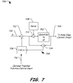
- FIG. 7 is a block diagram of a particular illustrative embodiment of a sigma-delta circuit adapted for use as a shaped random pulse sequence generator that is programmable to produce a random pulse sequence having a particular spectral shape;
- FIG. 8 is a block diagram of a system including a pulse edge control circuit that is responsive to a data generator, such as the sigma-delta circuit illustrated in FIG. 7 , to selectively phase shift or to selectively chop at least one PWM signal according to values associated with the random pulse sequence to produce at least one modulated PWM output having the particular spectral shape;
- a data generator such as the sigma-delta circuit illustrated in FIG. 7
- FIG. 9 is a graph of a particular illustrative example of a common mode power spectrum associated with a modulated PWM output signal produced by selectively chopping or not chopping a PWM signal and its duty cycle complement (within limits of time quantization effects) according to values of a random pulse sequence produced by a data generator, such as the sigma-delta circuit illustrated in FIG. 7 ; and
- FIG. 10 is a flow diagram of a particular illustrative embodiment of a method of shaping an output power spectrum associated with at least one modulated PWM output signal.
- FIG. 4 is a timing diagram 400 of a particular illustrative embodiment of a chop/no chop carrier suppression operation that can be selectively applied to suppress carrier power of a modulated PWM output signal and to spread carrier energy to frequencies other than the carrier frequency and its associated harmonics within a PWM output spectrum.
- the timing diagram 400 includes a high side signal (P) 402 and a low side signal (N) 404 , which have a differential mode component represented by signal 406 and a common mode component represented by signal 408 .
- the common mode component (signal 408 ) has a peak amplitude centered at a center of the frame.
- the timing diagram 400 also includes a chopped version of the high and low side signals (P and N) 402 and 404 , represented by the high side signal (P′) 412 and the low side signal (N′) 414 .
- the common mode signal 418 is inverted and the differential mode signal 416 remains unchanged (relative to the differential mode signal 406 ).
- the differential mode signal 406 or 416 determines the audio performance in an audio application, and the common mode signal 408 is what is predominantly responsible for electromagnetic interference (EMI).
- EMI electromagnetic interference
- by selectively chopping and not chopping a PWM input signal and its duty cycle complement PWM signal the common mode carrier energy at the carrier frequency is reduced over a sequence of frames, reducing EMI and radio frequency interference.
- the term “duty cycle complement” refers to a signal that, when aggregated with the PWM input signal, aggregates to an entire width of the PWM frame (within limits of time quantization effects).
- the term “chop” or “chop operation” refers to a technique that inverts the PWM input signal and its duty cycle complement and interchanges them to produce a modulated PWM output.
- the chop operation is alternately applied every other frame (e.g., a first PWM pulse is not chopped and a second PWM pulse is chopped)
- a resulting common mode carrier energy associated with the PWM P and N signals 402 and 404 and their inverted and swapped (interchanged) versions PWM P′ and N′ signals 412 and 414 ) averages to zero at the carrier frequency.
- FIG. 5 is a graph of a particular illustrative embodiment of a timing diagram 500 illustrating a quarter frame phase shift of a single pulse-width modulated (PWM) signal to suppress a carrier at the frame rate.
- the timing diagram 500 includes a PWM D signal 502 that is centered (positioned) within the frame at T/2. Over a two frame interval, the PWM D signal 502 is shifted. In one example, the PWM D signal 502 is shifted left (by ⁇ T/4) then right (by +T/4), as illustrated at 504 . In another example, the PWM D signal 502 is shifted right (by +T/4) then left (by ⁇ T/4), as illustrated at 506 .
- the above example represents a quarter-frame symmetrical pulse shift with no wrap-around.
- both signals may be shifted to abut the frame boundary, such that the PWM D signal 502 is shifted by less than a quarter of the frame width and the PWM B signal is shifted by more than a quarter of the frame width.
- the sum of the PWM D signal 502 and PWM B signal over two frames has zero content at the frame repetition rate in the Fourier Transform, which cancels the carrier in the common mode signal.
- This particular example can be referred to as a quarter frame asymmetrical pulse shifting with no wrap-around.
- the PWM D signal 502 can be shifted by plus or minus a quarter of the frame, and any portion of the PWM D signal 502 that crosses the frame boundary can be wrapped to an opposing frame boundary within the same PWM frame.
- This alternative example can be referred to as a quarter-frame symmetrical pulse shift with wrap-around.
- a pulse edge control circuit may be adapted to selectively apply a carrier suppression operation that includes selectively shifting one or more PWM signals by plus or minus a quarter of the frame width using quarter-frame symmetrical pulse shifting with no wrap-around, quarter-frame asymmetrical pulse shifting with no wrap-around, or quarter-frame symmetrical pulse shifting with wrap-around, depending on the implementation.
- FIG. 6 is a graph of an illustrative embodiment of a particular spectral shape 600 of a shaped random pulse sequence that can be used to define the power spectrum of at least one PWM input signal to produce at least one modulated PWM output signal having a desired spectral shape.
- the spectral shape 600 includes two band-stop regions, one with attenuation from 0-20 kHz resulting from nulls or notches at DC (0 kHz) and near 20 kHz (generally indicated at 602 ), and a second with attenuation around a selected frequency of interest resulting from nulls or notches at 200 kHz+/ ⁇ 10 kHz (generally indicated at 604 and 606 ).
- FIG. 7 is a block diagram of a particular illustrative embodiment of a sigma-delta circuit 700 adapted for use as a shaped random pulse sequence generator that produces a random pulse sequence having a programmable spectral shape, such as the particular spectral shape 600 illustrated in FIG. 6 .
- the stop-band at 200 kHz+/ ⁇ 10 kHz in FIG. 6 can be programmed for specific locations to reduce PWM radiation in desired frequency bands.
- the sigma-delta circuit 700 includes a quantizer 702 to produce a random pulse sequence having values of plus or minus one at an output 704 .
- the sigma-delta circuit 700 further includes a feedback loop 705 that has a transfer function (1 ⁇ G(z)) 706 .
- the transfer function 706 is programmable via a transfer function control input 716 to alter the transfer function of the feedback loop 705 .
- the sigma-delta circuit 700 includes a noise input 708 and a signal input 710 having a zero input value.
- the signal input 710 is coupled to a first summing node 712 that produces a first result that is a difference between a feedback value received from the feedback loop 705 (from the transfer function 706 ) and the zero input value.
- the first result is provided to a summing node 724 , which subtracts a value at the output 704 from the first result to produce a feedback result that is provided to the transfer function 706 .
- the first result is provided to a second summing node 714 , which adds the first result to a noise signal from the noise input 708 to produce a second result.
- the second result is provided to the quantizer 702 .
- the sigma-delta circuit 700 can be implemented as digital circuits, analog circuits, firmware, or any combination thereof.
- the transfer function 706 is configurable (programmable) via the transfer function control input 716 to produce a particular spectral shape, which may or may not have notches at particular frequencies.
- the random pulse sequence at the output 704 is consequently shaped by the transfer function 706 .
- the output 704 may be coupled to a pulse edge control circuit that is adapted to selectively apply a carrier suppression operation (such as a selective phase shift operation or a selective chop/no chop operation) according to values of the random pulse sequence.
- FIG. 8 is a block diagram of a system 800 including a pulse edge control circuit 806 that is adapted to apply a carrier suppression operation to an input PWM signal according to values of a shaped random pulse sequence generator to produce at least one modulated PWM output having the particular spectral shape as defined by the data generator.
- the system 800 includes a pulse-width modulated (PWM) source 802 that provides at least one PWM signal 804 to a pulse edge control circuit 806 .
- PWM pulse-width modulated
- the system 800 also includes the sigma-delta circuit 700 illustrated in FIG. 7 that provides a random sequence with a particular spectral shape 704 to the pulse edge control circuit 806 .
- the resulting output spectrum of signal 808 is effectively the convolution of the input PWM spectrum with the spectrum of the random pulse sequence.
- the pulse edge control circuit 806 is adapted to selectively phase shift the at least one PWM signal 804 by plus or minus a quarter of a PWM frame width relative to a center of the PWM frame at integer sub-multiples of a frame repetition rate.
- the pulse edge control circuit 806 is adapted to selectively chop or not chop the at least one PWM signal 804 .
- the shift or the chop can be selectively applied by the pulse edge control circuit 806 based on values of the random pulse sequence with the particular spectral shape 704 .
- the resulting modulated PWM output signal has a suppressed carrier energy at the carrier frequency, which energy is spread to other frequencies and the overall spectral shape at 808 is defined by the spectral shape of the data generator output, 700 .
- FIG. 9 is a graph of a particular illustrative example of a power spectrum 900 of the output PWM signal 808 in FIG. 8 .
- the programmable stop-band was set to be 200 kHz and the PWM frame rate is 960 kHz.
- the common mode power spectrum 900 has been spread as compared to the common mode power spectrum 300 illustrated in FIG. 3 . Further, the common mode power spectrum 900 does not include large common mode components that contribute to AM interference (AMI) or electromagnetic interference (EMI).
- AMI AM interference
- EMI electromagnetic interference
- the common mode power spectrum 900 includes little noise in the audio frequency band, and notches have been placed at n*960 kHz+/ ⁇ 200 kHz, where n is a non-negative integer, as indicated at 904 , 906 , 908 , 910 , and 912 .
- the graph 900 includes a notch at 0 kHz and at 20 kHz, as indicated at 902 . In an alternate example, should the programmable stop-band be centered at 300 kHz, the notches would be located at n*960 kHz+/ ⁇ 300 k Hz.
- FIG. 10 is a flow diagram of a particular illustrative embodiment of a method of shaping an output power spectrum associated with at least one modulated PWM output signal.
- PWM pulse-width modulated
- a random pulse sequence having a particular spectral shape is received from a data generator.
- the particular spectral shape includes notches at selected frequencies.
- a carrier suppression operation is applied to selectively phase shift or to selectively chop the received at least one PWM input signal according to values of the random pulse sequence to produce at least one modulated PWM output signal with a desired spectral shape as defined by the random pulse sequence.
- the at least one modulated PWM output signal has carrier energy that is spread to frequencies other than a carrier frequency and its harmonics.
- the carrier suppression operation can be applied at integer sub-multiples of a PWM frame repetition rate or at a rate that is faster than the frame repetition rate. The method terminates at 1008 .
- the method further includes programming the data generator to produce the particular spectral shape.
- the data generator includes a feedback loop having a programmable transfer function.
- the data generator has a nominally white noise input. The data generator shapes the white noise source to produce an output pulse sequence having the desired spectral shape often with notches at programmable frequency locations.
- a circuit device is disclosed that is adapted to utilize a random data sequence having a particular spectral shape to control application of a carrier suppression operation.
- a pulse edge control circuit selectively phase shifts a pulse-width modulated (PWM) input signal and its PWM duty cycle complement by plus or minus a quarter of a frame width at integer sub-multiples of a frame repetition rate based on values of the random data sequence.
- the pulse edge control circuit selectively chops (i.e., chops or does not chop) at least one PWM input signal based on values of the random data sequence.
- the resulting modulated PWM output has an altered carrier spectrum that has a spectral shape defined by the particular spectral shape of the random data sequence, including any frequency notches in the particular spectral shape.
- the resulting modulated PWM output signal has reduced carrier energy at a carrier frequency and at harmonics of the carrier frequency and exhibits reduced AM interference (AMI) and reduced electromagnetic interference (EMI) with respect to adjacent circuitry.
- AMI AM interference
- EMI reduced electromagnetic interference
Landscapes
- Amplifiers (AREA)
Abstract
Description
DM(t)=P(t)−N(t) (Equation 1).
As shown, in the “not chopped” version, the common mode component (signal 408) has a peak amplitude centered at a center of the frame. The
CM(t)=(P(t)+N(t))/2 (Equation 2).
N′(t)=−P(t) (Equation 3).
The low side signal (N) 404 is inverted and swapped with the high side signal (P) 402 becomes the high side signal (P′) 412, as shown by the following equation:
P′(t)=−N(t) (Equation 4).
In the chopped version, the
DM′(t)=P′(t)−N′(t)=−N(t)−−P(t)=DM(t) (Equation 5).
However, the
CM′(t)=(−N(t)−P(t))/2=−CM(t) (Equation 6).
Claims (22)
Priority Applications (3)
| Application Number | Priority Date | Filing Date | Title |
|---|---|---|---|
| US12/208,535 US7724105B2 (en) | 2008-04-01 | 2008-09-11 | System and method of shaping a power spectrum in PWM amplifiers |
| DE200910015782 DE102009015782A1 (en) | 2008-04-01 | 2009-03-31 | Circuit device for use in pulse-width modulated carrier suppressing system in class D amplifier, has pulse edge controller providing modulated pulse-width modulation signal to output of pulse edge controller |
| US12/767,605 US8188804B2 (en) | 2008-04-01 | 2010-04-26 | System and method of shaping a power spectrum in PWM amplifiers |
Applications Claiming Priority (2)
| Application Number | Priority Date | Filing Date | Title |
|---|---|---|---|
| US7256308P | 2008-04-01 | 2008-04-01 | |
| US12/208,535 US7724105B2 (en) | 2008-04-01 | 2008-09-11 | System and method of shaping a power spectrum in PWM amplifiers |
Related Child Applications (1)
| Application Number | Title | Priority Date | Filing Date |
|---|---|---|---|
| US12/767,605 Continuation US8188804B2 (en) | 2008-04-01 | 2010-04-26 | System and method of shaping a power spectrum in PWM amplifiers |
Publications (2)
| Publication Number | Publication Date |
|---|---|
| US20090243745A1 US20090243745A1 (en) | 2009-10-01 |
| US7724105B2 true US7724105B2 (en) | 2010-05-25 |
Family
ID=41116216
Family Applications (5)
| Application Number | Title | Priority Date | Filing Date |
|---|---|---|---|
| US12/126,125 Expired - Fee Related US7598895B1 (en) | 2008-04-01 | 2008-05-23 | System and method of altering a PWM carrier power spectrum |
| US12/208,535 Expired - Fee Related US7724105B2 (en) | 2008-04-01 | 2008-09-11 | System and method of shaping a power spectrum in PWM amplifiers |
| US12/543,888 Active US7821440B2 (en) | 2008-04-01 | 2009-08-19 | System and method of altering a PWM carrier power spectrum |
| US12/767,605 Active 2028-12-08 US8188804B2 (en) | 2008-04-01 | 2010-04-26 | System and method of shaping a power spectrum in PWM amplifiers |
| US12/895,804 Expired - Fee Related US7924200B2 (en) | 2008-04-01 | 2010-09-30 | System and method of altering a PWM carrier power spectrum |
Family Applications Before (1)
| Application Number | Title | Priority Date | Filing Date |
|---|---|---|---|
| US12/126,125 Expired - Fee Related US7598895B1 (en) | 2008-04-01 | 2008-05-23 | System and method of altering a PWM carrier power spectrum |
Family Applications After (3)
| Application Number | Title | Priority Date | Filing Date |
|---|---|---|---|
| US12/543,888 Active US7821440B2 (en) | 2008-04-01 | 2009-08-19 | System and method of altering a PWM carrier power spectrum |
| US12/767,605 Active 2028-12-08 US8188804B2 (en) | 2008-04-01 | 2010-04-26 | System and method of shaping a power spectrum in PWM amplifiers |
| US12/895,804 Expired - Fee Related US7924200B2 (en) | 2008-04-01 | 2010-09-30 | System and method of altering a PWM carrier power spectrum |
Country Status (2)
| Country | Link |
|---|---|
| US (5) | US7598895B1 (en) |
| CN (2) | CN101667820B (en) |
Cited By (2)
| Publication number | Priority date | Publication date | Assignee | Title |
|---|---|---|---|---|
| US20100171540A1 (en) * | 2008-04-01 | 2010-07-08 | Silicon Laboratories, Inc. | System and Method of Changing a PWM Power Spectrum |
| US20100296671A1 (en) * | 2008-04-01 | 2010-11-25 | Silicon Laboratories, Inc. | System and Method of Changing a PWM Power Spectrum |
Families Citing this family (25)
| Publication number | Priority date | Publication date | Assignee | Title |
|---|---|---|---|---|
| US8284963B2 (en) * | 2007-09-11 | 2012-10-09 | Texas Instruments Incorporated | Method and apparatus for diminishing mismatch effects between switched signals |
| US7598895B1 (en) * | 2008-04-01 | 2009-10-06 | Silicon Laboratories, Inc. | System and method of altering a PWM carrier power spectrum |
| KR20100008749A (en) * | 2008-07-16 | 2010-01-26 | 삼성전자주식회사 | Switching power amplifier and control method thereof |
| US8374233B2 (en) * | 2008-09-25 | 2013-02-12 | Intel Mobile Communications GmbH | IQ-modulation system and method for switched amplifiers |
| EP2533417B1 (en) * | 2010-02-03 | 2016-07-20 | Toyota Jidosha Kabushiki Kaisha | Apparatus for controlling rotating electrical machine and method for controlling rotating electrical machine |
| US8130128B2 (en) | 2010-03-30 | 2012-03-06 | Silicon Laboratores Inc. | System and method for generating shaped noise |
| KR101037167B1 (en) * | 2010-05-26 | 2011-05-26 | (주)아이엠피 | Carrier Noise Reduction Device in Digital Amplifier |
| DE102011118044A1 (en) * | 2011-11-09 | 2013-05-16 | Conti Temic Microelectronic Gmbh | Method for controlling a motor by means of pulse width modulation (PWM) |
| DE102011121139B4 (en) * | 2011-12-15 | 2016-11-24 | IAD Gesellschaft für Informatik, Automatisierung und Datenverarbeitung mbH | Device having a delta-sigma modulator and a MOSFET output stage connected thereto |
| TWI484415B (en) * | 2011-12-30 | 2015-05-11 | Chroma Ate Inc | Solar cell array simulator to adapt to the control method of photovoltaic inverter |
| CN103199721B (en) * | 2012-01-05 | 2015-04-01 | 致茂电子(苏州)有限公司 | Control method for enabling solar cell array simulator to be adapted to photovoltaic inverter |
| FR2988353B1 (en) * | 2012-03-21 | 2014-05-16 | Valeo Systemes Dessuyage | METHOD AND DEVICE FOR CONTROLLING A MOTOR VEHICLE WIPER ENGINE |
| US9059793B2 (en) * | 2013-01-28 | 2015-06-16 | Qualcomm Incorporated | Noise shaping for switching circuitry |
| US9325284B2 (en) * | 2013-02-02 | 2016-04-26 | Avago Technologies General Ip (Singapore) Pte. Ltd. | Radio frequency composite Class-S power amplifier having discrete power control |
| CN104022762B (en) * | 2013-02-28 | 2018-05-08 | 德克萨斯仪器股份有限公司 | The pulse-width modulator of phase average |
| JP6510199B2 (en) * | 2014-08-19 | 2019-05-08 | ローム株式会社 | Switching circuit, audio amplifier integrated circuit, electronic device, driving method of electroacoustic transducer |
| US20160149733A1 (en) * | 2014-11-26 | 2016-05-26 | Applied Materials, Inc. | Control architecture for devices in an rf environment |
| US9872341B2 (en) | 2014-11-26 | 2018-01-16 | Applied Materials, Inc. | Consolidated filter arrangement for devices in an RF environment |
| DE102017124575A1 (en) * | 2017-10-20 | 2019-04-25 | Dr. Ing. H.C. F. Porsche Aktiengesellschaft | Carrier modulated pulse width modulation to adjust the distortion spectrum of a clocked power electronics |
| CN107733403B (en) * | 2017-10-26 | 2021-05-11 | 中国人民解放军国防科技大学第六十三研究所 | Specific harmonic elimination multilevel radio frequency pulse width modulation method and modulator |
| FR3078457A1 (en) * | 2018-02-27 | 2019-08-30 | Stmicroelectronics (Grenoble 2) Sas | ENGINE CONTROL SYSTEM |
| CN111244957B (en) * | 2020-03-10 | 2021-04-13 | 石家庄赫伯孙电气有限公司 | Active power filter control algorithm based on voltage closed-loop control |
| CN111711223B (en) * | 2020-05-13 | 2023-08-04 | 许昌开普检测研究院股份有限公司 | Hybrid Space Vector Modulation Method for Improving Photovoltaic Inverter Efficiency and Harmonic Performance |
| CN118400026B (en) * | 2024-06-28 | 2024-08-23 | 北京天元特通科技有限公司 | VSAT TDMA signal superframe segmentation method based on channel power and related equipment |
| WO2026065429A1 (en) * | 2024-09-30 | 2026-04-02 | 深圳市汇顶科技股份有限公司 | Signal processing method, circuit and chip, and electronic device |
Citations (40)
| Publication number | Priority date | Publication date | Assignee | Title |
|---|---|---|---|---|
| US5014016A (en) | 1989-04-13 | 1991-05-07 | Beltone Electronics Corporation | Switching amplifier |
| US5247581A (en) | 1991-09-27 | 1993-09-21 | Exar Corporation | Class-d bicmos hearing aid output amplifier |
| US5389829A (en) | 1991-09-27 | 1995-02-14 | Exar Corporation | Output limiter for class-D BICMOS hearing aid output amplifier |
| US5672998A (en) | 1995-08-09 | 1997-09-30 | Harris Corporation | Class D amplifier and method |
| US5798672A (en) | 1995-07-13 | 1998-08-25 | Sgs-Thomson Microelectronics S.R.L. | Single-output dual-supply class D amplifier |
| US6097249A (en) | 1998-09-02 | 2000-08-01 | Rockford Corporation | Method and device for improved class BD amplification having single-terminal alternating-rail dual-sampling topology |
| US6127885A (en) | 1998-08-31 | 2000-10-03 | Cello, Limited | Class D amplifiers including transition zone modulation |
| US6160455A (en) | 1998-03-10 | 2000-12-12 | Indigo Manufacturing Inc. | Derived power supply for composite bridge amplifiers |
| US6297692B1 (en) | 1996-10-31 | 2001-10-02 | Bang & Olufsen A/S | Pulse modulation power amplifier with enhanced cascade control method |
| US20030020539A1 (en) | 2001-07-27 | 2003-01-30 | Tokihiko Sawashi | Power amplifier apparatus |
| US20030067348A1 (en) | 2001-10-09 | 2003-04-10 | Joel Butler | Class d switching audio amplifier |
| US6552606B1 (en) | 1999-01-12 | 2003-04-22 | Technische Universiteit Eindhoven | Amplifier circuit having output filter capacitance current feedback |
| US6552607B1 (en) | 2001-11-12 | 2003-04-22 | Apogee Technology Inc. | Time division multiplexed PWM amplifier |
| US20030122615A1 (en) | 2003-01-03 | 2003-07-03 | Zeff Robert Terry | Improved Class BD Amplifier |
| US6594309B1 (en) | 1999-02-11 | 2003-07-15 | Stmicroelectronics S.R.L. | PWM power amplifier with digital input |
| US6597240B1 (en) | 2001-04-02 | 2003-07-22 | Cirrus Logic, Inc. | Circuits and methods for slew rate control and current limiting in switch-mode systems |
| US20040232978A1 (en) | 2003-05-23 | 2004-11-25 | Easson Craig Alexander | Filterless class D amplifiers using spread spectrum PWM modulation |
| US20040232979A1 (en) | 2003-05-23 | 2004-11-25 | Edwards Christopher Francis | Efficient minimum pulse spread spectrum modulation for filterless class d amplifiers |
| US20050054307A1 (en) | 2001-04-27 | 2005-03-10 | Watts Robert David | Signal processing circuit |
| US20050083116A1 (en) | 2003-10-15 | 2005-04-21 | Texas Instruments Incorporated | Detection of DC output levels from a class D amplifier |
| US20050083114A1 (en) | 2003-10-15 | 2005-04-21 | Texas Instruments Incorporated | Recovery from clipping events in a class D amplifier |
| US20050083115A1 (en) | 2003-10-15 | 2005-04-21 | Texas Instruments Incorporated | Soft transitions between muted and unmuted states in class D audio amplifiers |
| US20050099231A1 (en) | 2003-11-06 | 2005-05-12 | Marvell International Ltd. | Class d amplifier |
| US20050116770A1 (en) | 2003-08-11 | 2005-06-02 | Larry Kirn | Multi-reference switching amplifier modulation method and apparatus |
| US20050200404A1 (en) | 2002-07-10 | 2005-09-15 | Derek Bernardon | Amplifier circuit |
| US20060008095A1 (en) | 2004-07-02 | 2006-01-12 | Yamaha Corporation | Pulse-width modulation amplifier and suppression of clipping therefor |
| US20060077007A1 (en) | 2003-03-10 | 2006-04-13 | Guillaume De Cremoux | Three state class d amplifier |
| US20060103458A1 (en) | 2004-11-12 | 2006-05-18 | Texas Instruments Incorporated | On-the-fly introduction of inter-channel delay in a pulse-width-modulation amplifier |
| US7119629B2 (en) | 2001-12-21 | 2006-10-10 | Bang & Olufsen Icepower A/S | Synchronized controlled oscillation modulator |
| US20060226904A1 (en) | 2005-04-08 | 2006-10-12 | Nalbant Mehmet K | Minimum on time, dual supply class D amplifiers with ground speaker returns and methods of class D amplification |
| US20060279354A1 (en) | 2005-06-13 | 2006-12-14 | Texas Instruments, Inc. | Reduction of audible artifacts in an audio system |
| US20070002943A1 (en) | 2005-06-20 | 2007-01-04 | Freescale Semiconductor, Inc. | Suppressed carrier quadrature pulse modulator |
| US20070024365A1 (en) | 2005-07-29 | 2007-02-01 | Texas Instruments, Inc. | Class-D amplifier system |
| US20070146069A1 (en) | 2005-12-27 | 2007-06-28 | Kuo-Hung Wu | Filterless class D power amplifier |
| US20070229159A1 (en) | 2006-04-04 | 2007-10-04 | Jagadeesh Krishnan | Multi-mode class-D amplifiers |
| US7298209B1 (en) | 2003-11-06 | 2007-11-20 | Marvell World Trade Ltd. | Class D amplifier |
| US7301417B2 (en) | 2004-03-25 | 2007-11-27 | Digian Technology, Inc. | Pulse width modulation method and apparatus |
| US20080042743A1 (en) | 2006-08-17 | 2008-02-21 | Matsushita Electric Industrial Co., Ltd. | Differential input class d amplifier |
| US7561002B1 (en) * | 2005-04-26 | 2009-07-14 | Pulsecore Semiconductor, Inc. | Method and apparatus for frequency modulating a periodic signal of varying duty cycle |
| US7598895B1 (en) * | 2008-04-01 | 2009-10-06 | Silicon Laboratories, Inc. | System and method of altering a PWM carrier power spectrum |
Family Cites Families (9)
| Publication number | Priority date | Publication date | Assignee | Title |
|---|---|---|---|---|
| US5872998A (en) * | 1995-11-21 | 1999-02-16 | Seiko Epson Corporation | System using a primary bridge to recapture shared portion of a peripheral memory of a peripheral device to provide plug and play capability |
| HK1041621A1 (en) * | 1998-11-30 | 2002-07-12 | 邦及奥卢夫森发电站公司 | A pulse width modulation power converter |
| US6614297B2 (en) * | 2001-07-06 | 2003-09-02 | Texas Instruments Incorporated | Modulation scheme for filterless switching amplifiers with reduced EMI |
| US20030210009A1 (en) * | 2002-05-10 | 2003-11-13 | Analog Devices, Inc. | Pulse width modulated drive system for electronically commutated motors |
| CN1174543C (en) * | 2002-06-21 | 2004-11-03 | 浙江大学 | Phase Shift Control Bidirectional DC-DC Converter |
| JP4060745B2 (en) * | 2003-04-16 | 2008-03-12 | シャープ株式会社 | Locking mechanism for opening / closing member and image forming apparatus |
| DE10350336B4 (en) * | 2003-10-29 | 2006-06-08 | Infineon Technologies Ag | Method and apparatus for pulse width modulation |
| JP4618017B2 (en) * | 2004-07-02 | 2011-01-26 | ヤマハ株式会社 | Clip suppression circuit for pulse width modulation amplifier |
| US7791521B2 (en) * | 2008-04-01 | 2010-09-07 | Silicon Laboratories, Inc. | System and method of changing a PWM power spectrum |
-
2008
- 2008-05-23 US US12/126,125 patent/US7598895B1/en not_active Expired - Fee Related
- 2008-09-11 US US12/208,535 patent/US7724105B2/en not_active Expired - Fee Related
-
2009
- 2009-03-31 CN CN200910132927XA patent/CN101667820B/en not_active Expired - Fee Related
- 2009-04-01 CN CN2009101299132A patent/CN101572535B/en not_active Expired - Fee Related
- 2009-08-19 US US12/543,888 patent/US7821440B2/en active Active
-
2010
- 2010-04-26 US US12/767,605 patent/US8188804B2/en active Active
- 2010-09-30 US US12/895,804 patent/US7924200B2/en not_active Expired - Fee Related
Patent Citations (57)
| Publication number | Priority date | Publication date | Assignee | Title |
|---|---|---|---|---|
| US5014016A (en) | 1989-04-13 | 1991-05-07 | Beltone Electronics Corporation | Switching amplifier |
| US5247581A (en) | 1991-09-27 | 1993-09-21 | Exar Corporation | Class-d bicmos hearing aid output amplifier |
| US5389829A (en) | 1991-09-27 | 1995-02-14 | Exar Corporation | Output limiter for class-D BICMOS hearing aid output amplifier |
| US5798672A (en) | 1995-07-13 | 1998-08-25 | Sgs-Thomson Microelectronics S.R.L. | Single-output dual-supply class D amplifier |
| US5672998A (en) | 1995-08-09 | 1997-09-30 | Harris Corporation | Class D amplifier and method |
| US6297692B1 (en) | 1996-10-31 | 2001-10-02 | Bang & Olufsen A/S | Pulse modulation power amplifier with enhanced cascade control method |
| US6160455A (en) | 1998-03-10 | 2000-12-12 | Indigo Manufacturing Inc. | Derived power supply for composite bridge amplifiers |
| US6127885A (en) | 1998-08-31 | 2000-10-03 | Cello, Limited | Class D amplifiers including transition zone modulation |
| US6097249A (en) | 1998-09-02 | 2000-08-01 | Rockford Corporation | Method and device for improved class BD amplification having single-terminal alternating-rail dual-sampling topology |
| US6552606B1 (en) | 1999-01-12 | 2003-04-22 | Technische Universiteit Eindhoven | Amplifier circuit having output filter capacitance current feedback |
| US6594309B1 (en) | 1999-02-11 | 2003-07-15 | Stmicroelectronics S.R.L. | PWM power amplifier with digital input |
| US6597240B1 (en) | 2001-04-02 | 2003-07-22 | Cirrus Logic, Inc. | Circuits and methods for slew rate control and current limiting in switch-mode systems |
| US20050054307A1 (en) | 2001-04-27 | 2005-03-10 | Watts Robert David | Signal processing circuit |
| US7046080B2 (en) | 2001-04-27 | 2006-05-16 | Robert David Watts | Signal processing circuit |
| US20030020539A1 (en) | 2001-07-27 | 2003-01-30 | Tokihiko Sawashi | Power amplifier apparatus |
| US6653897B2 (en) | 2001-07-27 | 2003-11-25 | Sony Corporation | Power amplifier apparatus |
| US20040169552A1 (en) | 2001-10-09 | 2004-09-02 | Joel Butler | Class d switching audio amplifier |
| US6794932B1 (en) | 2001-10-09 | 2004-09-21 | Evenstar, Inc. | Class D switching audio amplifier |
| US6563377B2 (en) | 2001-10-09 | 2003-05-13 | Evenstar, Inc. | Class D switching audio amplifier |
| US20030067348A1 (en) | 2001-10-09 | 2003-04-10 | Joel Butler | Class d switching audio amplifier |
| US6552607B1 (en) | 2001-11-12 | 2003-04-22 | Apogee Technology Inc. | Time division multiplexed PWM amplifier |
| US7119629B2 (en) | 2001-12-21 | 2006-10-10 | Bang & Olufsen Icepower A/S | Synchronized controlled oscillation modulator |
| US20050200404A1 (en) | 2002-07-10 | 2005-09-15 | Derek Bernardon | Amplifier circuit |
| US7068095B2 (en) | 2002-07-10 | 2006-06-27 | Infineon Technologies Ag | Amplifier circuit |
| US20030122615A1 (en) | 2003-01-03 | 2003-07-03 | Zeff Robert Terry | Improved Class BD Amplifier |
| US7230485B2 (en) | 2003-03-10 | 2007-06-12 | Nxp B.V. | Three state class D amplifier |
| US20060077007A1 (en) | 2003-03-10 | 2006-04-13 | Guillaume De Cremoux | Three state class d amplifier |
| US6847257B2 (en) | 2003-05-23 | 2005-01-25 | Maxim Integrated Products, Inc. | Efficient minimum pulse spread spectrum modulation for filterless class D amplifiers |
| US20040232979A1 (en) | 2003-05-23 | 2004-11-25 | Edwards Christopher Francis | Efficient minimum pulse spread spectrum modulation for filterless class d amplifiers |
| US20040232978A1 (en) | 2003-05-23 | 2004-11-25 | Easson Craig Alexander | Filterless class D amplifiers using spread spectrum PWM modulation |
| US20050116770A1 (en) | 2003-08-11 | 2005-06-02 | Larry Kirn | Multi-reference switching amplifier modulation method and apparatus |
| US7142049B2 (en) | 2003-08-11 | 2006-11-28 | Jam Technologies, Inc. | Multi-reference switching amplifier modulation method and apparatus |
| US20050083115A1 (en) | 2003-10-15 | 2005-04-21 | Texas Instruments Incorporated | Soft transitions between muted and unmuted states in class D audio amplifiers |
| US7078964B2 (en) | 2003-10-15 | 2006-07-18 | Texas Instruments Incorporated | Detection of DC output levels from a class D amplifier |
| US20050083114A1 (en) | 2003-10-15 | 2005-04-21 | Texas Instruments Incorporated | Recovery from clipping events in a class D amplifier |
| US7142050B2 (en) | 2003-10-15 | 2006-11-28 | Texas Instruments Incorporated | Recovery from clipping events in a class D amplifier |
| US20050083116A1 (en) | 2003-10-15 | 2005-04-21 | Texas Instruments Incorporated | Detection of DC output levels from a class D amplifier |
| US7298209B1 (en) | 2003-11-06 | 2007-11-20 | Marvell World Trade Ltd. | Class D amplifier |
| US20050099231A1 (en) | 2003-11-06 | 2005-05-12 | Marvell International Ltd. | Class d amplifier |
| US7190224B2 (en) | 2003-11-06 | 2007-03-13 | Marvell World Trade Ltd. | Class D amplifier |
| US7242248B1 (en) | 2003-11-06 | 2007-07-10 | Marvell World Trade Ltd. | Class D amplifier |
| US7301417B2 (en) | 2004-03-25 | 2007-11-27 | Digian Technology, Inc. | Pulse width modulation method and apparatus |
| US20060008095A1 (en) | 2004-07-02 | 2006-01-12 | Yamaha Corporation | Pulse-width modulation amplifier and suppression of clipping therefor |
| US20060103458A1 (en) | 2004-11-12 | 2006-05-18 | Texas Instruments Incorporated | On-the-fly introduction of inter-channel delay in a pulse-width-modulation amplifier |
| US20060226904A1 (en) | 2005-04-08 | 2006-10-12 | Nalbant Mehmet K | Minimum on time, dual supply class D amplifiers with ground speaker returns and methods of class D amplification |
| US7218173B2 (en) | 2005-04-08 | 2007-05-15 | Maxim Integrated Products, Inc. | Minimum on time, dual supply class D amplifiers with ground speaker returns and methods of class D amplification |
| US7561002B1 (en) * | 2005-04-26 | 2009-07-14 | Pulsecore Semiconductor, Inc. | Method and apparatus for frequency modulating a periodic signal of varying duty cycle |
| US7279965B2 (en) | 2005-06-13 | 2007-10-09 | Thomas Holm Hansen | Reduction of audible artifacts in an audio system |
| US20060279354A1 (en) | 2005-06-13 | 2006-12-14 | Texas Instruments, Inc. | Reduction of audible artifacts in an audio system |
| US20070002943A1 (en) | 2005-06-20 | 2007-01-04 | Freescale Semiconductor, Inc. | Suppressed carrier quadrature pulse modulator |
| US20070024365A1 (en) | 2005-07-29 | 2007-02-01 | Texas Instruments, Inc. | Class-D amplifier system |
| US7262658B2 (en) | 2005-07-29 | 2007-08-28 | Texas Instruments Incorporated | Class-D amplifier system |
| US20070146069A1 (en) | 2005-12-27 | 2007-06-28 | Kuo-Hung Wu | Filterless class D power amplifier |
| US7332962B2 (en) | 2005-12-27 | 2008-02-19 | Amazion Electronics, Inc. | Filterless class D power amplifier |
| US20070229159A1 (en) | 2006-04-04 | 2007-10-04 | Jagadeesh Krishnan | Multi-mode class-D amplifiers |
| US20080042743A1 (en) | 2006-08-17 | 2008-02-21 | Matsushita Electric Industrial Co., Ltd. | Differential input class d amplifier |
| US7598895B1 (en) * | 2008-04-01 | 2009-10-06 | Silicon Laboratories, Inc. | System and method of altering a PWM carrier power spectrum |
Non-Patent Citations (3)
| Title |
|---|
| "U.S. Appl. No. 12/126,125, Notice of Allowance mailed Jun. 2, 2009", 7 pgs. |
| Kempski, A., et al., "Decomposition of EMI Noise into Common and Differential Modes in PWM Inverter Drive System", Electrical Power Quality and Utilization Journal, V. XII, N. 1, (2006), 6 pgs. |
| Ogasawara, S., et al., "Suppression of Common Mode Voltage in a PWM Rectifier/Inverter System", Dept. of Electrical Engineering, Tokyo Institute of Technology, IEEE, (2001), 2015-2021. |
Cited By (4)
| Publication number | Priority date | Publication date | Assignee | Title |
|---|---|---|---|---|
| US20100171540A1 (en) * | 2008-04-01 | 2010-07-08 | Silicon Laboratories, Inc. | System and Method of Changing a PWM Power Spectrum |
| US20100296671A1 (en) * | 2008-04-01 | 2010-11-25 | Silicon Laboratories, Inc. | System and Method of Changing a PWM Power Spectrum |
| US7965214B2 (en) | 2008-04-01 | 2011-06-21 | Silicon Laboratories Inc. | System and method of changing a PWM power spectrum |
| US8154358B2 (en) * | 2008-04-01 | 2012-04-10 | Silicon Laboratories, Inc. | System and method of changing a PWM power spectrum |
Also Published As
| Publication number | Publication date |
|---|---|
| US20090243903A1 (en) | 2009-10-01 |
| CN101667820A (en) | 2010-03-10 |
| US20110019728A1 (en) | 2011-01-27 |
| US8188804B2 (en) | 2012-05-29 |
| US7924200B2 (en) | 2011-04-12 |
| CN101667820B (en) | 2013-11-13 |
| CN101572535B (en) | 2013-12-04 |
| US20100207699A1 (en) | 2010-08-19 |
| US7821440B2 (en) | 2010-10-26 |
| US7598895B1 (en) | 2009-10-06 |
| CN101572535A (en) | 2009-11-04 |
| US20090309654A1 (en) | 2009-12-17 |
| US20090243745A1 (en) | 2009-10-01 |
Similar Documents
| Publication | Publication Date | Title |
|---|---|---|
| US7724105B2 (en) | System and method of shaping a power spectrum in PWM amplifiers | |
| US7791521B2 (en) | System and method of changing a PWM power spectrum | |
| US8130128B2 (en) | System and method for generating shaped noise | |
| US8154358B2 (en) | System and method of changing a PWM power spectrum | |
| EP3836392A1 (en) | Switched capacitor transmitter circuits and methods | |
| EP1985013A4 (en) | Systems and methods for improving performance in a digital amplifier by adding an ultrasonic signal to an input audio signal | |
| KR20120018794A (en) | Multi-bit class-d power amplifier system | |
| EP1384317B1 (en) | A signal processing circuit | |
| US20110037517A1 (en) | Concept, method and apparatus of improved distortion switched-mode amplifier | |
| US7932790B2 (en) | Switched modulation of a radio-frequency amplifier | |
| Ruotsalainen et al. | A new quadrature PWM modulator with tunable center frequency for digital RF transmitters | |
| US7994853B2 (en) | Class-D amplifier with dual feedback loop | |
| TW201203965A (en) | Multi-level pulse modulated polar transmitter and method for generating multi-level modulated envelope signals carrying phase information within | |
| EP3044920A1 (en) | Switched-mode high-linearity transmitter using pulse width modulation | |
| US8116368B2 (en) | PWM signal generator, PWM signal generating device, and digital amplifier | |
| Ruotsalainen et al. | Quantization noise cancelation scheme for digital quadrature RF pulse encoding | |
| Arian et al. | High dynamic range pseudo–two‐level digital pulse‐width modulation for power‐efficient RF transmitters | |
| Morgan | Combined Three-State/PWM Signal Coding for Wideband High-Efficiency Class-S Amplifiers | |
| KR20240088208A (en) | Transmitter and transmission method based on BFSK modulation using waveform shaping | |
| Ma et al. | Optimal Delta-Sigma Modulation Based Noise Shaping for Truly Aliasing-Free digital PWM | |
| Maehata et al. | Asymmetrical waveform compensation for concurrent dual-band 1-bit band-pass delta-sigma modulator with a quasi-elliptic filter | |
| Yoneya | Pulse width and position modulation for fully digital audio amplifier | |
| Chung et al. | Outphasing Multi-Level RF PWM for Inter-Band Carrier Aggregation in Digital Transmitters | |
| Chung et al. | Adaptive noise cancellation with concurrent multi-band delta-sigma modulation for digital transmitters | |
| KR20170128433A (en) | Method for Amplifying an Input Signal |
Legal Events
| Date | Code | Title | Description |
|---|---|---|---|
| AS | Assignment |
Owner name: SILICON LABORATORIES INC., TEXAS Free format text: ASSIGNMENT OF ASSIGNORS INTEREST;ASSIGNORS:ALDERSON, JEFFREY D.;KHOURY, JOHN M.;BEALE, RICHARD G.;REEL/FRAME:021519/0267;SIGNING DATES FROM 20080909 TO 20080910 Owner name: SILICON LABORATORIES INC.,TEXAS Free format text: ASSIGNMENT OF ASSIGNORS INTEREST;ASSIGNORS:ALDERSON, JEFFREY D.;KHOURY, JOHN M.;BEALE, RICHARD G.;SIGNING DATES FROM 20080909 TO 20080910;REEL/FRAME:021519/0267 |
|
| FEPP | Fee payment procedure |
Free format text: PAYOR NUMBER ASSIGNED (ORIGINAL EVENT CODE: ASPN); ENTITY STATUS OF PATENT OWNER: LARGE ENTITY |
|
| REMI | Maintenance fee reminder mailed | ||
| LAPS | Lapse for failure to pay maintenance fees | ||
| STCH | Information on status: patent discontinuation |
Free format text: PATENT EXPIRED DUE TO NONPAYMENT OF MAINTENANCE FEES UNDER 37 CFR 1.362 |
|
| STCH | Information on status: patent discontinuation |
Free format text: PATENT EXPIRED DUE TO NONPAYMENT OF MAINTENANCE FEES UNDER 37 CFR 1.362 |
|
| FP | Lapsed due to failure to pay maintenance fee |
Effective date: 20140525 |