US7723872B2 - Method and apparatus for determining a switching time for an electrical switching device - Google Patents
Method and apparatus for determining a switching time for an electrical switching device Download PDFInfo
- Publication number
- US7723872B2 US7723872B2 US11/815,124 US81512406A US7723872B2 US 7723872 B2 US7723872 B2 US 7723872B2 US 81512406 A US81512406 A US 81512406A US 7723872 B2 US7723872 B2 US 7723872B2
- Authority
- US
- United States
- Prior art keywords
- voltage
- oscillation
- time
- determining
- driving voltage
- Prior art date
- Legal status (The legal status is an assumption and is not a legal conclusion. Google has not performed a legal analysis and makes no representation as to the accuracy of the status listed.)
- Expired - Fee Related, expires
Links
Images


Classifications
-
- H—ELECTRICITY
- H01—ELECTRIC ELEMENTS
- H01H—ELECTRIC SWITCHES; RELAYS; SELECTORS; EMERGENCY PROTECTIVE DEVICES
- H01H9/00—Details of switching devices, not covered by groups H01H1/00 - H01H7/00
- H01H9/54—Circuit arrangements not adapted to a particular application of the switching device and for which no provision exists elsewhere
- H01H9/56—Circuit arrangements not adapted to a particular application of the switching device and for which no provision exists elsewhere for ensuring operation of the switch at a predetermined point in the ac cycle
- H01H2009/566—Circuit arrangements not adapted to a particular application of the switching device and for which no provision exists elsewhere for ensuring operation of the switch at a predetermined point in the ac cycle with self learning, e.g. measured delay is used in later actuations
Definitions
- the invention relates to a method and an apparatus for determining a switching time for an electrical switching device having an interrupter gap which is arranged between a first line section, to which a driving voltage is applied, and a second line section, which forms a resonant circuit after a disconnection process of the switching device.
- the waveform of an alternating voltage should ideally be sinusoidal and should oscillate at a predetermined frequency and with a predetermined amplitude.
- transient overvoltages can occur during a switching process, caused by inductive and/or capacitive elements. Transient overvoltages such as these are superimposed on the rated frequency and the rated amplitude of the ideal alternating voltage, and interfere with the desired voltage profile.
- Switching operations often represent a triggering event for the occurrence of overvoltages.
- the invention is therefore based on the object of specifying a method and an apparatus for determining a switching time, by means of which the occurrence of transient overvoltages and oscillations in an electrical power transmission system is limited.
- the object is achieved according to the invention in that a time profile of the driving voltage is determined after a disconnection process of the electrical switching device, a time profile of an oscillation voltage which occurs in the resonant circuit after the disconnection process of the electrical switching device is determined, a time profile of a resultant voltage, which corresponds to the difference between the driving voltage and the oscillation voltage, is determined, and at least one rise in the driving voltage and at least one rise in the oscillation voltage are evaluated, and a switching time is defined as a function of the rises and the time profile of the resultant voltage.
- the object is also achieved in that a time profile of the driving voltage is determined after a disconnection process of the electrical switching device, a time profile of an oscillation voltage which occurs in the resonant circuit after the disconnection process of the electrical switching device is determined, a time profile of an oscillation current which flows in the resonant circuit after the disconnection process of the electrical switching device is determined, a time profile of a resultant voltage, which corresponds to the difference between the driving voltage and the oscillation voltage, is determined, and at least one rise in the driving voltage and at least one polarity of the oscillation current are evaluated, and a switching time is defined as a function of the at least one rise in the driving voltage and the at least one polarity of the oscillation current, and the time profile of the resultant voltage.
- the resultant voltage that occurs may have considerably higher voltage amplitudes than the driving voltage, because of the components contained in the resonant circuit, such as coils and capacitors. This is particularly due to the fact that inductances and capacitances are energy storage elements, which cause time delays. Considerably excessive peak values can therefore occur as a result of poor combinations. These high voltage peaks have disadvantageous effects on the insulation system. The insulation is therefore dielectrically more heavily loaded than in the rated conditions. This results in the insulation aging more quickly. Particularly in the case of solid-insulated line sections such as cables, this can adversely affect the life. In extreme situations, the voltage peaks may be so high that flashovers occur on the lines.
- flashovers may be expressed, for example, as partial discharges or arcs on holding insulators for cross-country overhead lines insulated in the open air.
- phenomena such as these are particularly disadvantageous in solid-insulated insulation systems such as cables, since irreparable damage can occur there.
- the time profile of the resultant voltage is thus a major criterion for defining the switching time of an electrical switching device.
- the choice of the switching time can be optimized by taking account of the rises, that is to say the gradient of the rise in the driving voltage as well as the gradient of the rise in the oscillation voltage which is formed in the resonant circuit.
- the profile of the resultant voltage is in each case considered at a specific time, and the profile of the oscillation voltage and/or of the driving voltage is evaluated at the same time.
- a switching time at which the occurrence of overvoltages is limited particularly effectively can be defined as a function of the rises in the driving voltage and/or in the oscillation voltage and the time profile of the resultant voltage.
- Various methods can be used to determine the time profiles of the driving voltage, of the oscillation voltage and of the resultant voltage and/or the oscillation current.
- voltage transformers and current transformers can be used on the appropriate line sections for this purpose.
- the data can therefore be recorded in real time, the corresponding voltage/current profiles can be determined and a switching time can be defined.
- the rise in the voltage profiles may, for example, be obtained by differentiation of the time profile at the appropriate time of interest.
- Electronic data processing devices can be used to determine a first derivative at virtually any desired time within a very short time, and thus to determine the rise in the driving voltage and/or the oscillation voltage.
- One advantageous refinement of the invention can also provide for the switching time to be in the vicinity of a zero crossing of the resultant voltage.
- an alternating voltage or a plurality of alternating voltages which are phase-shifted with respect to one another in a common system, is or are often used as the driving voltage.
- Systems with a plurality of alternating voltages that are related to one another are also referred to as polyphase alternating voltage systems.
- the driving voltage which applies voltage to the first line section, is typically at a constant frequency. Roughly speaking, the frequency ranges that are preferably used are 162 ⁇ 3 Hz, 50 Hz, 60 Hz and other frequency ranges.
- the lowest overvoltages during a switching process can be assumed to occur in each case in the area of the zero crossing of the resultant voltage. The zero crossings of the resultant voltage are therefore chosen as preferred switching times.
- a further advantageous refinement makes it possible to provide for the vicinity of a zero crossing of the resultant voltage for the switching time to be chosen at which the driving voltage has a negative rise and the oscillation current has a positive polarity, or the driving voltage has a positive rise and the oscillation current has a negative polarity.
- the resultant voltage has a comparatively large number of voltage zero crossings. In this case, it has been found that some of these voltage zero crossings represent a better switching time than others.
- One criterion for choice of the most suitable voltage zero crossings of the resultant voltage is represented by the rises in the driving voltages and the rises in the oscillation voltages. If the rises in the driving voltage and in the oscillation voltage have the same direction sense at a zero crossing of the resultant voltage, then this zero crossing is particularly suitable for use as a switching time.
- the expression the same rises means that the driving voltage and the oscillation voltage each have a positive rise, or each have a negative rise.
- the numerical magnitude of the rise can also be included in the evaluation process, thus making it possible to define the switching time more accurately.
- One particularly suitable switching time is a zero crossing of the resultant voltage at which the driving voltage has a negative rise and the oscillation current has a positive polarity, or at which the driving voltage has a positive rise and the oscillation current has a negative polarity.
- a further advantageous refinement makes it possible for the oscillation current to flow through a compensation inductance.
- overhead lines are used in electrical power transmission systems.
- a capacitor arrangement is formed between the overhead line that is carrying high voltage and the ground potential underneath the overhead line.
- the overhead line can act as a capacitor, and appropriate charging power must be introduced into the overhead line.
- compensation inductors are coils which have an appropriate inductance, and compensate for the capacitive load produced by the overhead line.
- These inductors may be designed differently so that, for example, they can be grounded as required, or else their inductance can be varied.
- Switchable inductors are preferably used at the start and at the end of an overhead line.
- such constellations can also occur in underground cable systems in which a corresponding capacitive impedance is formed between the electrical conductor and the cable sheath.
- the compensation inductor also governs the magnitude of the oscillation current in the second line section.
- the components which are actually present and the resistance resulting from the conductor material that is used result in impedance losses, remagnetization losses, etc. so that the oscillation current and the oscillation voltage are damped in the second line section.
- a further advantageous refinement variant makes it possible to provide for the time profile of the oscillation voltage and/or of the oscillation current to be determined by means of a Prony method.
- the interrupter gap is closed when the switching device is connected.
- the first line section with the driving voltage drives a current into the second line section.
- the driving voltage is produced by means of a generator in a power station.
- the driving voltage that is applied results in this voltage propagating in the second line section as well.
- Loads are typically connected in the second line section. By way of example, these may be motors, heaters or else complete system sections, such as industrial consumers or a large number of households.
- the driving voltage is now still present only in the first line section, since the interrupter gap has been opened and the driving voltage can no longer propagate in the second line section.
- the first line section typically contains power-generating devices such as driving supply systems with corresponding generators and/or power stations.
- An oscillation voltage is produced in the second system section, corresponding to its constellation with resistive, inductive and/or capacitive components, resulting from the sudden disconnection of the interrupter gap and the rates of change associated with this, and this oscillation voltage drives an oscillation current.
- the time profile of the driving voltage is in this case determined relatively easily, since it can be assumed that this is a rigid system in which the driving voltage is the governing variable and remains approximately constant. It is more problematic to determine the profile of the oscillation current and/or oscillation voltage in the resonant circuit. In order to have an appropriate time profile, it is desirable to make a reliable prediction of the profile for one or more future intervals from measured values determined within a short interval. By way of example, a Prony method can be used for this purpose.
- the Prony method offers the advantage over other methods, for example Laplace transformation, of allowing a comparatively accurate prediction of further voltage and/or current profiles to be made from a small number of measured values.
- the Prony method is suitable for carrying out controlled switching in a particular manner since, in comparison to a Fourier transformation, the sampling time period for the available voltage and/or current data is independent of the fundamental frequency to be expected. Furthermore, when using the Prony method, the phase shift and the damping of the individual frequency components can be recorded as required.
- the available voltage and/or current data must first of all be determined in the electrical system at different times. This is based on N complex data points x[1], . . . x[N] of any desired sinusoidal or exponentially damped event. These data points must be equidistant data points. This sampled process can be described by a summation of p exponential functions:
- Equation (2.1) A simpler representation of Equation (2.1) is obtained by combination of the parameters into time-dependent and time-independent parameters.
- h k A k ⁇ exp ⁇ ( j ⁇ k ) ( 2.4 )
- z k exp ⁇ [ ( ⁇ k + j2 ⁇ ⁇ ⁇ f k ) ⁇ T ] ( 2.5 )
- the parameter h k is the complex amplitude and represents a time-independent constant.
- the complex exponent z k is a time-dependent parameter.
- Equation (2.8) The aim of the Prony algorithm has been shown in Equation (2.8). A more comprehensive representation of the equation for 1 ⁇ n ⁇ p is given in Equation (2.9).
- Equation (2.8) is the solution of a homogeneous linear differential equation with constant coefficients.
- the parameter z to be determined indicates the zeros of the polynomial.
- the polynomial is represented as a summation with the aid of the fundamental algebra rule (Equation 2.11).
- Equation (2.11) The polynomial from Equation (2.11) can be seen again in the right-hand part of the summation.
- the zeros that are sought are obtained by determining all the roots z k .
- Equation (2.15) is the sought linear differential equation, whose solution is Equation (2.8).
- the polynomial (2.11) is the characteristic equation for the differential equation.
- Equation (2.16) There are p unknowns in Equation (2.16).
- the matrix x comprises p+1 rows and columns. Equation (2.16) is therefore overdefined.
- the upper row in the matrix x, and therefore also the known coefficient a[0], is deleted, and the first column is subtracted.
- the p unknowns can be determined by using the p equations.
- the Prony method can thus be combined in three steps.
- Solution of Equation (2.17) results in the coefficients of the polynomial (2.11)
- (2.20) ⁇ k tan ⁇ 1 [Im ( h k )/ Re ( h k )] (2.21)
- the further profile of the input signal can also be “predicted” using the parameters z k and h k , Equation (2.8) and a change in the variable n, which reflects the time period to be estimated. If there is a difference in the time step width for the estimation in comparison to that for sampling, the parameters damping, frequency, amplitude and phase shift must, however, be determined explicitly.
- a further advantage of the Prony method for analysis of current and/or voltage profiles is that it can also be used for high-frequency processes.
- the expression high-frequency processes should be understood to mean processes which oscillate in the range from 100 to 700 Hz.
- the operating frequency range covers the frequencies between 24 and 100 Hz. Frequencies below 24 Hz should be understood as being low frequencies.
- High-frequency processes occur, for example, when switching devices are switched. The high-frequency components are superimposed on the fundamental frequency.
- the modified Prony method is similar to the maximum likelihood principle (Gaussian principle of least squares). The calculation is based on a fixed p (number of exponential functions, see above). An iteration process is carried out during the calculation, thus optimizing the accuracy of the voltage and/or current profiles to be predicted. The degree of accuracy of the prediction can be varied by defining tolerance limits for the optimization process. The computation time required can thus be reduced depending on the requirement.
- the modified Prony method is described in detail in Osborne, Smyth: A modified Prony Algorithm for fitting functions defined by difference equations, SIAM Journal of Scientific and Statistical Computing, volume 12, 362-382, March 1991.
- the modified Prony method is insensitive to “noise” in the voltage and/or current data determined from the electrical power supply system. “Noise” such as this is unavoidable when using actual components for determining the voltage and/or current data. Interference such as this can be minimized only with an unreasonably large amount of effort.
- the robustness to “noise” in the input signals means that the modified Prony method allows the use of low-cost test equipment for determining the available voltage and/or current data in the electrical system.
- An apparatus can be provided for carrying out the method as described above, which has means for automated processing of the voltage and/or current data, using the Prony methods.
- a further advantageous refinement makes it possible to provide for the voltage across the interrupter gap after a disconnection process to correspond to the resultant voltage.
- the interrupter gap must produce an impedance change as quickly as possible from an ideally infinitely large impedance to an infinitely low impedance, or vice versa. Ideally, this should take place suddenly. However, this is not the case in present technical systems.
- Switching elements with contact pieces which can move relative to one another and are located in an insulating gas are used in the high-voltage field.
- This insulating gas is preferably sulfur hexafluoride at an increased pressure.
- a certain recovery time is required in which contaminated arc quenching gas formed in the switching gap is removed from the switching gap and replaced by uncontaminated insulating gas.
- the resultant voltage which is formed across the interrupter gap results from the driving voltage applied to one side of the interrupter gap and the oscillation voltage applied to the other side of the interrupter gap. Since, as has been stated above, time delays occur when oscillation processes occur in the resonant circuit, considerably higher voltage magnitudes can occur across the interrupter gap than the rated voltage of the driving voltage would lead one to suppose.
- the resultant voltage which occurs across the interrupter gap of the electrical switching device therefore represents a significant variable, which is used to define a switching time for an electrical switching device.
- the electrical switching device also has to reliably cope with an excessive voltage.
- a further advantageous refinement can provide that the switching time is defined in the vicinity of any desired zero crossing of the resultant voltage in the event of progressive damping of the oscillation voltage and/or of the oscillation current.
- the oscillation voltage and/or the oscillation current in the resonant circuit are damped by the actual components contained in the resonant circuit, such as capacitors, coils and resistors. If the damping is sufficiently heavy, it is no longer sensibly possible to carry out any measurement, so that it is possible to dispense with the evaluation of the rises in the oscillation voltage and/or in the driving voltage and/or in the polarity of the oscillation current. In order to allow rapid switching, this is then just based on the zero crossings of the resultant voltage, with switching taking place at the next-possible zero crossing of the resultant voltage. If the damping of the oscillation voltage or of the oscillation current is progressive, the effects of an excessive voltage across the interrupter gap of the electrical switching device are negligible.
- the switching time is advantageously possible to provide for the switching time to be used for a connection process for the electrical switching device.
- the invention also relates to an apparatus for carrying out the method mentioned initially.
- the object of the invention in this case is to specify an apparatus which allows selection of a switching time.
- the apparatus has a device for comparing the rise in the driving voltage and the oscillation voltage, and/or the polarity of the oscillation current.
- a device for comparing the rise in the driving voltage and the oscillation voltage and/or the polarity of the oscillation current allows simple selection of the potential switching times with respect to the voltage zero crossings of the resultant voltage.
- the result of a comparison such as this may, for example, be a yes or no decision on the permissibility of a switching process.
- FIG. 1 shows an outline illustration of a voltage profile with optimum switching times
- FIG. 2 shows a schematic design of an electrical power transmission system
- FIG. 3 shows the profiles of two different resultant voltages
- FIG. 4 shows a profile of different voltages and currents
- FIG. 5 shows a profile of different voltages
- FIG. 6 shows the timing for determining a future voltage/current profile
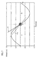
- FIG. 7 shows how a pre-arcing characteristic is taken into account for a capacitive load
- FIG. 8 shows the use of a pre-arcing characteristic for an inductive load on an interrupter gap in an electrical switching device
- FIG. 9 shows a device for comparing voltage profiles.
- FIG. 1 shows a sinusoidal profile of an alternating voltage whose frequency is 50 Hz.
- inductive loads should in each case be switched as far as possible at the voltage maximum of a sinusoidal voltage profile (times 5 ms, 15 ms).
- capacitive loads should in each case be switched during a voltage zero crossing, in order to avoid charging processes on a capacitor (times 0 ms, 10 ms, 20 ms).
- FIG. 2 shows a fundamental design of a line section within an electrical power transmission system.
- An electrical switching device has an interrupter gap 1 .
- the interrupter gap is formed from two contact pieces which can move relative to one another.
- a first line section 2 and a second line section 3 can be connected to one another and disconnected from one another via the interrupter gap 1 .
- the first line section 2 has a generator 4 .
- the generator 4 produces a driving voltage which, for example, is a 50 Hz alternating voltage in a polyphase voltage system.
- the second line section 3 has an overhead line 5 .
- the overhead line 5 can be connected at its first end by means of a first inductor 6 to ground potential 7 , and at its second end via a second inductor 8 to ground potential 7 .
- inductor 9 it is also possible to provide for a further inductor 9 to be connected to the second inductor 8 .
- Different variants of the inductors 6 , 8 , 9 can be connected to ground potential 7 by means of different switching devices 10 . It is therefore possible to compensate the overhead line 5 to different extents, depending on the load situation. For example, the capacitive impedance
- a compensation degree k can be determined from the ratio of the capacitive impedance X c of the overhead line and the inductive impedance X Lres of all the inductors.
- the inductors 6 , 8 , 9 can be connected differently with respect to one another in order to set the compensation degree k. However, it is also possible to provide for the inductors to have a variable inductive impedance X L .
- plunger-type core inductors may be used for this purpose.
- a resonant circuit can be formed via ground potential 7 in the second line section 3 .
- corresponding current paths must be formed via the switching devices 10 to ground potential 7 in the second line section 3 .
- a resonant circuit is formed from the inductive and capacitive impedances, and an oscillation current can flow in the resonant circuit, driven by an oscillation voltage.
- FIG. 3 shows the resultant voltage profiles formed across the interrupter gap 1 for different compensation degrees.
- a compensation degree of 0.3 results in a correspondingly different frequency profile, although this once again has a multiplicity of voltage zero crossings.
- connection resistors which were previously provided in order to limit overvoltages.
- Better switching results can thus be achieved by the definition of an optimum reconnection time, that is to say reduced transient overvoltages occur than when the connection of an electrical switching device with connection resistors is controlled arbitrarily.
- FIG. 4 shows the evaluation and determination of a switching time for an electrical switching device using the driving voltage A, the oscillation voltage B, the resultant voltage C and the oscillation current D.
- the driving voltage A oscillates at a constant frequency and with a constant amplitude.
- the oscillation voltage B which occurs on the second line section 3 in the resonant circuit oscillates at a specific frequency, which is variable, and with variable amplitudes. This variability is the result of the fact that damping occurs in the system and additional external influences can be superimposed.
- the superimposition of the driving voltage A on the first line section 2 and the oscillation voltage B which occurs in the second line section 3 results in a time profile of a resultant voltage C.
- the resultant voltage C corresponds to the voltage across the open interrupter gap.
- the resultant voltage C oscillates with a considerably variable amplitude, and there is a phase shift both with respect to the driving voltage A and with respect to the oscillation voltage B. Potential switching times occur at the voltage zero crossings of the resultant voltage C.
- the voltage zero crossings are marked with crosses in order that they can be seen more easily in the profile of the resultant voltage C.
- the voltage zero crossings of the resultant voltage C are not all suitable for a reconnection process for the interrupter gap 1 .
- the polarity of the oscillation current D is also used as a selection criterion in the examples illustrated in FIG. 4 .
- the polarity of the oscillation current D is in each case marked with a plus or a minus in the corresponding intervals between the current zero crossings of the oscillation current D.
- a positive polarity of the oscillation current D occurs at the first voltage zero crossing of the resultant voltage D, together with a positive rise in the driving voltage A, that is to say the first voltage zero crossing 1 of the resultant voltage C is not suitable for a connection process.
- a negative rise in the driving voltage A occurs at the fourteenth voltage zero crossing of the resultant voltage C, and the oscillation current D has a positive polarity, that is to say, of the voltage zero crossings, the fourteenth voltage zero crossing of the resultant voltage C is particularly suitable for a reconnection process.
- the first and the fourteenth voltage zero crossings are in this case used only by way of example. Furthermore, other voltage zero crossings may also be particularly suitable for a connection process for the interrupter gap 1 . These may be located within the interval illustrated in FIG. 4 , or else outside this interval.
- FIG. 5 shows an alternative selection method, in which A 1 illustrates the time profile of the driving voltage, B 1 the time profile of the oscillation voltage, and C 1 the resultant voltage across the interrupter unit.
- the resultant voltage C 1 results from the potential difference between the driving voltage A 1 applied to the first line section 2 and the oscillation voltage B 1 on the second line section side 3 of the interrupter gap 1 .
- the zero crossings of the resultant voltage C 1 once again represent potential switching times.
- the rises (gradients of the rise) at these times are in each case evaluated in order to choose the most suitable voltage zero crossings of the resultant voltage C 1 .
- both the driving voltage A 1 and the oscillation voltage B 1 have a negative rise, that is to say this time is particularly suitable for a reconnection process.
- the driving voltage A 1 has a negative rise and the oscillation voltage C 1 has a positive rise, that is to say the time t 2 and the zero crossing of the resultant voltage C 1 that occurs at this time are not suitable for a reconnection process.
- every other zero crossing of the resultant voltage can be classified on the basis in the respectively associated rises in the driving voltage and oscillation voltage, thus resulting in even more suitable and unsuitable zero crossings of the resultant voltage for a reconnection process.
- FIG. 6 shows a time sequence for sampling X, calculation Y, monitoring Z, renewed calculation U and the time interval for tripping V.
- the future profile of the oscillation voltage and/or of the oscillation current is calculated, resulting in a future profile of the resultant voltage profile.
- the time interval from 100 to 150 ms it is possible to compare the values determined by calculation for the oscillation voltage, oscillation current and resultant voltage, driving voltage, in terms of their time profile, with the values which have actually already occurred. If the values determined by calculation are confirmed within the time window provided for monitoring, it is assumed that the signal profiles have been calculated correctly in advance.
- a Prony method or similar methods can be used for calculation.
- a time interval from 150 to 200 ms is now still available in which the future voltage and/or current profiles can be recalculated with the assistance of the voltage and/or current profiles determined in the actual network within the time interval from 0 to 150 ms.
- a more accurate calculation of the future time profile of the currents and/or of the voltages can be obtained on the basis of the greater time interval from 0 to 150 ms and the greater number of available measured values.
- An ideal switching time can now be defined as a function of the voltage zero crossings of the resultant voltage as well as the rises in the oscillation voltage and in the driving voltage, and/or in the driving voltage and the polarity of the oscillation current that occurs.
- a time profile for emitting a tripping signal can now be produced as a function of the switching time, in which case it is possible to take account of the pre-arcing characteristic of the interrupter gap 1 being used, so that reconnection of the interrupter unit takes place at the latest after 300 or 500 ms, at a time at which any excessive voltages within the electrical power transmission system are limited. Reconnection can be carried out particularly quickly if the time profiles illustrated by way of example in FIGS. 4 and 5 are calculated in advance within a very short interval (50 ms or less). This advance determination allows an adequate lead time in which all of the necessary waiting times or lead times can be included.
- FIGS. 7 and 8 each show a pre-arcing characteristic 11 for the interrupter gap 1 .
- the pre-arcing characteristic 11 is illustrated in a simplified form as a linear profile with a specific gradient.
- the intention in FIG. 7 is to switch a capacitive load, for example an unloaded cable.
- a capacitive load is preferably intended to be switched within a voltage zero crossing.
- the voltage has a sinusoidal profile.
- the pre-arcing characteristic 11 is sufficiently steep that an intersection of the voltage profile and of the pre-arcing characteristic 11 ideally coincides at a voltage zero crossing.
- the pre-arcing characteristic 11 a and the voltage profile intercept approximately at the time 5 ms, that is to say pre-arcing would occur even at this time, as a consequence of which, however, the ideal time for initiating an electric current occurs in advance of the voltage zero crossing.
- an electrical switching device should be used which has a comparatively steep pre-arcing characteristic.
- the conductive contact between the contact pieces and the pre-arcing coincide at the time 10 ms, and allow the electrical switching device to be switched with virtually no overvoltage.
- the aim is to switch an inductive load.
- the pre-arcing characteristic 11 is, however, sufficiently steep that the pre-arcing characteristic and the voltage profile necessarily intercept.
- An arc is struck, with pre-arcing, between the moving contact pieces of the interrupter gap 1 at the time 5 ms.
- the contact pieces which can move relative to one another touch at the time 7.6 ms.
- FIG. 9 shows a fundamental design of an apparatus for carrying out the method.
- the apparatus has a device 12 for comparing the rises in the driving voltage A and in the oscillation voltage B.
- a signal 13 is emitted when defined relationships between the rises occur.
Abstract
Description
where
-
- T—sampling period in s
- Ak—amplitude of the complex exponent
- ak—damping factor in s−1
- fk—frequency of the sinusoidal oscillation in Hz
- θk—phase shift in radians.
for 1≦n≦N. If there is an even number of exponential functions p, then p/2 damped cosine functions exist.
φp(z)=a[0]z p +a[1]z p−1 + . . . +a[p−1]z+a[p] (2.10)
a k=ln|z k |/T (2.18)
f k=tan−1 [Im(z k)/Re(z k)]/[2πT] (2.19)
A k =|h k| (2.20)
θk=tan−1 [Im(h k)/Re(h k)] (2.21)
of the overhead line can be overcompensated or else undercompensated for by the inductive impedance XL(XL=j·ω·L) of the inductors. A compensation degree k can be determined from the ratio of the capacitive impedance Xc of the overhead line and the inductive impedance XLres of all the inductors. The
Claims (22)
Applications Claiming Priority (4)
| Application Number | Priority Date | Filing Date | Title |
|---|---|---|---|
| DE102005005228A DE102005005228A1 (en) | 2005-01-31 | 2005-01-31 | Method and device for determining a switching time of an electrical switching device |
| DE102005005228.2 | 2005-01-31 | ||
| DE102005005228 | 2005-01-31 | ||
| PCT/EP2006/050236 WO2006082131A1 (en) | 2005-01-31 | 2006-01-17 | Method and device for determining a switching time of an electric switching device |
Publications (2)
| Publication Number | Publication Date |
|---|---|
| US20080211317A1 US20080211317A1 (en) | 2008-09-04 |
| US7723872B2 true US7723872B2 (en) | 2010-05-25 |
Family
ID=36096234
Family Applications (1)
| Application Number | Title | Priority Date | Filing Date |
|---|---|---|---|
| US11/815,124 Expired - Fee Related US7723872B2 (en) | 2005-01-31 | 2006-01-17 | Method and apparatus for determining a switching time for an electrical switching device |
Country Status (11)
| Country | Link |
|---|---|
| US (1) | US7723872B2 (en) |
| EP (1) | EP1844484B1 (en) |
| JP (1) | JP4629113B2 (en) |
| KR (1) | KR100933579B1 (en) |
| CN (1) | CN101111912B (en) |
| BR (1) | BRPI0606816A2 (en) |
| CA (1) | CA2596192C (en) |
| DE (2) | DE102005005228A1 (en) |
| RU (1) | RU2393572C2 (en) |
| UA (1) | UA90880C2 (en) |
| WO (1) | WO2006082131A1 (en) |
Cited By (1)
| Publication number | Priority date | Publication date | Assignee | Title |
|---|---|---|---|---|
| US11757282B2 (en) | 2018-09-28 | 2023-09-12 | Hitachi Energy Switzerland Ag | Method and device for controlling at least one circuit breaker of a power system |
Families Citing this family (12)
| Publication number | Priority date | Publication date | Assignee | Title |
|---|---|---|---|---|
| DE102008024420A1 (en) * | 2008-05-16 | 2009-11-19 | Siemens Aktiengesellschaft | Method for determining a switching time of an electrical switching device |
| BRPI0804330B1 (en) * | 2008-10-13 | 2019-03-12 | Universidade Estadual De Campinas - Unicamp | METHOD FOR FAST TRIPOLAR RELIGION IN DRIVING REACTIVE COMPENSATION LINES |
| EP2707958B1 (en) * | 2011-05-09 | 2015-11-18 | ABB Technology AG | Point-on-wave controller with at least three monitoring inputs |
| JP6045604B2 (en) | 2012-12-14 | 2016-12-14 | 三菱電機株式会社 | Power switching control device |
| WO2015056289A1 (en) * | 2013-10-15 | 2015-04-23 | 三菱電機株式会社 | Power-switchgear control device and pole-closure control method |
| WO2015056326A1 (en) * | 2013-10-17 | 2015-04-23 | 三菱電機株式会社 | Power-switchgear control device and pole-opening control method |
| CN105024377B (en) * | 2013-12-23 | 2019-01-22 | Abb技术有限公司 | The method and its controller of conversion are put on wave |
| CN104409280B (en) * | 2014-12-01 | 2017-01-25 | 深圳市宝安任达电器实业有限公司 | EPS (emergency power supply) power output control relay sparking prevention control method and circuit |
| DE102016117271B3 (en) | 2016-09-14 | 2018-03-15 | Phoenix Contact Gmbh & Co. Kg | Relay with a controller and method for controlling a relay |
| DE102016117273B4 (en) | 2016-09-14 | 2018-03-29 | Phoenix Contact Gmbh & Co. Kg | Relay with a controller and method for controlling a relay |
| CN113376515A (en) * | 2020-03-09 | 2021-09-10 | 西门子股份公司 | Method and device for determining closing time of circuit breaker and computer readable medium |
| RU2737047C1 (en) * | 2020-04-22 | 2020-11-25 | Общество с ограниченной ответственностью Научно-производственное предприятие "ЭКРА" | Method for automatic repeated switching of power lines with shunt reactors |
Citations (7)
| Publication number | Priority date | Publication date | Assignee | Title |
|---|---|---|---|---|
| US5627415A (en) * | 1993-03-18 | 1997-05-06 | Hydro-Quebec | System and method for opening/closing circuit breakers |
| EP1006538A1 (en) * | 1998-12-03 | 2000-06-07 | ABB Research Ltd. | Control and monitoring device for the opening/closing of electric operating elements |
| US6233132B1 (en) | 1998-09-03 | 2001-05-15 | Ranco Incorporated Of Delaware | Zero cross relay actuation method and system implementing same |
| US20030235017A1 (en) | 2002-06-24 | 2003-12-25 | Daniel Liu | Spark elimination circuit for controlling relay contacts |
| US20060285366A1 (en) * | 2005-05-23 | 2006-12-21 | Matthias Radecker | Control circuit for a switch unit of a clocked power supply circuit, and resonance converter |
| US7336461B2 (en) * | 2003-04-02 | 2008-02-26 | Areva T&D Sa | Method for determining the moment of closure of a circuit breaker on a high voltage line |
| US7626286B2 (en) * | 2002-04-05 | 2009-12-01 | Abb Technology Ag | Method for mains-synchronous switching of circuit breakers, and an apparatus for carrying out this method |
Family Cites Families (5)
| Publication number | Priority date | Publication date | Assignee | Title |
|---|---|---|---|---|
| JPS6180716A (en) * | 1984-09-28 | 1986-04-24 | 株式会社日立製作所 | Power system |
| JPH07192584A (en) * | 1993-12-28 | 1995-07-28 | Fuji Electric Co Ltd | Current zero point cutoff control method of ac switch |
| JP2000188044A (en) * | 1998-12-21 | 2000-07-04 | Mitsubishi Electric Corp | Phase control switching device |
| JP3986810B2 (en) * | 2001-12-03 | 2007-10-03 | 三菱電機株式会社 | Power switching control device |
| JP4452653B2 (en) * | 2005-06-07 | 2010-04-21 | 三菱電機株式会社 | Input phase detector for electromagnetic induction equipment |
-
2005
- 2005-01-31 DE DE102005005228A patent/DE102005005228A1/en not_active Withdrawn
-
2006
- 2006-01-17 KR KR1020077019997A patent/KR100933579B1/en not_active IP Right Cessation
- 2006-01-17 UA UAA200708771A patent/UA90880C2/en unknown
- 2006-01-17 CA CA 2596192 patent/CA2596192C/en not_active Expired - Fee Related
- 2006-01-17 US US11/815,124 patent/US7723872B2/en not_active Expired - Fee Related
- 2006-01-17 JP JP2007552620A patent/JP4629113B2/en not_active Expired - Fee Related
- 2006-01-17 WO PCT/EP2006/050236 patent/WO2006082131A1/en active Application Filing
- 2006-01-17 EP EP20060704214 patent/EP1844484B1/en not_active Not-in-force
- 2006-01-17 BR BRPI0606816-2A patent/BRPI0606816A2/en not_active IP Right Cessation
- 2006-01-17 DE DE200650008993 patent/DE502006008993D1/en active Active
- 2006-01-17 RU RU2007132724A patent/RU2393572C2/en not_active IP Right Cessation
- 2006-01-17 CN CN2006800036079A patent/CN101111912B/en not_active Expired - Fee Related
Patent Citations (7)
| Publication number | Priority date | Publication date | Assignee | Title |
|---|---|---|---|---|
| US5627415A (en) * | 1993-03-18 | 1997-05-06 | Hydro-Quebec | System and method for opening/closing circuit breakers |
| US6233132B1 (en) | 1998-09-03 | 2001-05-15 | Ranco Incorporated Of Delaware | Zero cross relay actuation method and system implementing same |
| EP1006538A1 (en) * | 1998-12-03 | 2000-06-07 | ABB Research Ltd. | Control and monitoring device for the opening/closing of electric operating elements |
| US7626286B2 (en) * | 2002-04-05 | 2009-12-01 | Abb Technology Ag | Method for mains-synchronous switching of circuit breakers, and an apparatus for carrying out this method |
| US20030235017A1 (en) | 2002-06-24 | 2003-12-25 | Daniel Liu | Spark elimination circuit for controlling relay contacts |
| US7336461B2 (en) * | 2003-04-02 | 2008-02-26 | Areva T&D Sa | Method for determining the moment of closure of a circuit breaker on a high voltage line |
| US20060285366A1 (en) * | 2005-05-23 | 2006-12-21 | Matthias Radecker | Control circuit for a switch unit of a clocked power supply circuit, and resonance converter |
Non-Patent Citations (3)
| Title |
|---|
| Lobos et al.: "Analysis of Power System Transients Using Wavelets and Prony Method", Power Tech Conference, 2001 IEEE Porto, Sep. 10-13, 2001. |
| Osborne et al.: "A Modified Prony Algorithm For Fitting Functions Defined By Difference Equations", SIAM Journal of Scientific and Statistical Computing, vol. 12, pp. 362-382, Mar. 1991. |
| S. Lawrence Marple, Jr.: "Digital Spectral Analysis with Applications", 1987. |
Cited By (1)
| Publication number | Priority date | Publication date | Assignee | Title |
|---|---|---|---|---|
| US11757282B2 (en) | 2018-09-28 | 2023-09-12 | Hitachi Energy Switzerland Ag | Method and device for controlling at least one circuit breaker of a power system |
Also Published As
| Publication number | Publication date |
|---|---|
| CN101111912A (en) | 2008-01-23 |
| CA2596192A1 (en) | 2006-08-10 |
| CN101111912B (en) | 2010-06-23 |
| CA2596192C (en) | 2014-06-17 |
| DE102005005228A1 (en) | 2006-08-31 |
| US20080211317A1 (en) | 2008-09-04 |
| KR100933579B1 (en) | 2009-12-22 |
| EP1844484B1 (en) | 2011-03-02 |
| RU2393572C2 (en) | 2010-06-27 |
| DE502006008993D1 (en) | 2011-04-14 |
| WO2006082131A1 (en) | 2006-08-10 |
| BRPI0606816A2 (en) | 2009-07-14 |
| JP2008529227A (en) | 2008-07-31 |
| EP1844484A1 (en) | 2007-10-17 |
| RU2007132724A (en) | 2009-03-10 |
| UA90880C2 (en) | 2010-06-10 |
| KR20070099682A (en) | 2007-10-09 |
| JP4629113B2 (en) | 2011-02-09 |
Similar Documents
| Publication | Publication Date | Title |
|---|---|---|
| US7723872B2 (en) | Method and apparatus for determining a switching time for an electrical switching device | |
| US20120095707A1 (en) | Method for Identifying Type of Fault on Power Line | |
| CN107677931B (en) | Fault rapid identification method based on DC waveform curvature change difference | |
| Jovcic | Series LC DC circuit breaker | |
| Jamali et al. | Detection of secondary arc extinction for adaptive single phase auto‐reclosing based on local voltage behaviour | |
| Schultz et al. | Improving interruption performance of mechanical circuit breakers by controlling pre‐current‐zero wave shape | |
| Bhatt et al. | Evaluation of controlled energisation of an unloaded power transformer for minimising the level of inrush current and transient voltage distortion using PIR‐CBs | |
| US7692336B2 (en) | Method for predicting a future voltage and/or current curve | |
| Martinez et al. | Parameter determination for modeling system transients-Part VI: Circuit breakers | |
| US20190296543A1 (en) | Method for detecting fault in power transmission line and protection system using the same | |
| Seyedi et al. | New controlled switching approach for limitation of transmission line switching overvoltages | |
| JP2001013197A (en) | Electrical apparatus testing device | |
| Ritter et al. | Prediction of bus-transfer switching in future HVdc substations | |
| CN116068333B (en) | Multi-criterion fusion fault line selection device and line selection method based on fuzzy theory | |
| US11828803B2 (en) | Method for testing capacitive current switching of a circuit breaker | |
| McBride et al. | Investigation of the Interaction between Substation Transients and Transformers in HV and EHV Applications | |
| Deyhim et al. | Insulation risk assessment of controlled switching considering pre‐strike voltage and line trapped charge | |
| CN113076643A (en) | Method and system for analyzing rapid transient overvoltage signal | |
| Pramudya et al. | Modelling of high voltage AC circuit breaker based on circuit breaker's technical data: Using Schwarz Black Box arc model | |
| Samitz-Ove et al. | On controlled switching of high voltage unloaded transmission lines | |
| Jayarathna et al. | An improved wide frequency model for vfto of power transformers using transfer functions | |
| Colclaser et al. | The traveling-wave approach to transient recovery voltage | |
| Acosta et al. | Field investigations into the factors governing the severity of prestriking transients | |
| Xin et al. | Dynamic arcing model of switching and its effect on VFTO | |
| Martinez‐Velasco et al. | Introduction to the Simulation of Electromagnetic Transients Using ATP |
Legal Events
| Date | Code | Title | Description |
|---|---|---|---|
| AS | Assignment |
Owner name: SIEMENS AKTIENGESELLSCHAFT,GERMANY Free format text: ASSIGNMENT OF ASSIGNORS INTEREST;ASSIGNORS:PILZ, GEORG;SCHEGNER, PETER;WALLNER, CHRISTIAN;SIGNING DATES FROM 20070625 TO 20070713;REEL/FRAME:024109/0276 Owner name: SIEMENS AKTIENGESELLSCHAFT, GERMANY Free format text: ASSIGNMENT OF ASSIGNORS INTEREST;ASSIGNORS:PILZ, GEORG;SCHEGNER, PETER;WALLNER, CHRISTIAN;SIGNING DATES FROM 20070625 TO 20070713;REEL/FRAME:024109/0276 |
|
| FPAY | Fee payment |
Year of fee payment: 4 |
|
| FEPP | Fee payment procedure |
Free format text: MAINTENANCE FEE REMINDER MAILED (ORIGINAL EVENT CODE: REM.) |
|
| LAPS | Lapse for failure to pay maintenance fees |
Free format text: PATENT EXPIRED FOR FAILURE TO PAY MAINTENANCE FEES (ORIGINAL EVENT CODE: EXP.) |
|
| STCH | Information on status: patent discontinuation |
Free format text: PATENT EXPIRED DUE TO NONPAYMENT OF MAINTENANCE FEES UNDER 37 CFR 1.362 |
|
| FP | Lapsed due to failure to pay maintenance fee |
Effective date: 20180525 |