US7720456B2 - Adjust switching rate of a power supply to mitigate interference - Google Patents
Adjust switching rate of a power supply to mitigate interference Download PDFInfo
- Publication number
- US7720456B2 US7720456B2 US11/355,477 US35547706A US7720456B2 US 7720456 B2 US7720456 B2 US 7720456B2 US 35547706 A US35547706 A US 35547706A US 7720456 B2 US7720456 B2 US 7720456B2
- Authority
- US
- United States
- Prior art keywords
- channel
- switching frequency
- interest
- power supply
- frequency
- Prior art date
- Legal status (The legal status is an assumption and is not a legal conclusion. Google has not performed a legal analysis and makes no representation as to the accuracy of the status listed.)
- Active, expires
Links
Images


Classifications
-
- H—ELECTRICITY
- H04—ELECTRIC COMMUNICATION TECHNIQUE
- H04B—TRANSMISSION
- H04B15/00—Suppression or limitation of noise or interference
- H04B15/005—Reducing noise, e.g. humm, from the supply
-
- H—ELECTRICITY
- H04—ELECTRIC COMMUNICATION TECHNIQUE
- H04B—TRANSMISSION
- H04B2215/00—Reducing interference at the transmission system level
- H04B2215/064—Reduction of clock or synthesizer reference frequency harmonics
- H04B2215/068—Reduction of clock or synthesizer reference frequency harmonics by avoiding a reception frequency range
Definitions
- This invention relates generally to radio receivers and more particularly to reducing receiver interference.
- the general architecture of a radio includes a radio receiver and a processor.
- the radio receiver receives a radio frequency (RF) signal and converts it into a baseband signal.
- the processor recovers embedded data of the RF signal from the baseband signal.
- RF radio frequency
- the radio receiver should be designed to mitigate the adverse affects of interfering signals external to the radio (e.g., adjacent channel interference) and to mitigate the adverse affects of interference from within the radio.
- adjacent channel interference the bandwidth of the radio receiver is relatively narrow such that signals outside of a frequency band of interest (i.e., adjacent channels) are substantially attenuated while signals within the frequency band of interest (i.e., the desired channel) are not attenuated.
- radio receivers include a plurality of techniques to reduce internal interference. For instance, radio receivers utilize component matching, synchronization, calibration, temperature compensation, etc.
- harmonics of the switching rate of a switch mode power supply falling within the frequency band of interest are not an issue since the frequency band of interest is significantly greater than the switching frequency such that the harmonics that may fall within the frequency band of interest are of negligible magnitude and/or because the switch mode power supply is physically, and thus, electromagnetically isolated from the radio receiver (e.g., the power supply is implemented on a different integrated circuit than the radio receiver).
- the harmonics of the switching rate of the switch mode power supply may adversely affect the performance of the radio receiver.
- FIG. 1 is a schematic block diagram of a radio in accordance with the present invention.
- FIG. 2 is a diagram illustrating adjusting the switching rate of a switch mode power supply in accordance with the present invention
- FIG. 3 is a schematic block diagram of an adjustable switching rate switch mode power supply in accordance with the present invention.
- FIG. 4 is a logic diagram of a method for mitigating interference from a switch mode power supply in accordance with the present invention
- FIG. 5 is a logic diagram of another method for mitigating interference from a switch mode power supply in accordance with the present invention.
- FIG. 6 is a logic diagram of yet another method for mitigating interference from a switch mode power supply in accordance with the present invention.
- FIG. 1 is a schematic block diagram of a radio 10 that includes a receiver section 12 , processing module 14 and a switch mode power supply 16 .
- the processing module 14 may be a single processing device or a plurality of processing devices. Such a processing device may be a microprocessor, micro-controller, digital signal processor, microcomputer, central processing unit, field programmable gate array, programmable logic device, state machine, logic circuitry, analog circuitry, digital circuitry, and/or any device that manipulates signals (analog and/or digital) based on operational instructions.
- the processing module 14 may further include an associated memory element that may be a single memory device, a plurality of memory devices, and/or embedded circuitry of the processing module.
- Such a memory device may be a read-only memory, random access memory, volatile memory, non-volatile memory, static memory, dynamic memory, flash memory, cache memory, and/or any device that stores digital information.
- the processing module implements one or more of its functions via a state machine, analog circuitry, digital circuitry, and/or logic circuitry
- the memory element storing the corresponding operational instructions may be embedded within, or external to, the circuitry comprising the state machine, analog circuitry, digital circuitry, and/or logic circuitry.
- the memory element stores, and the processing module 32 executes, operational instructions corresponding to at least some of the steps and/or functions illustrated in FIGS. 1-6 .
- the receiver section 12 receives a radio frequency (RF) signal 18 and converts them into a baseband signal 20 .
- the receiver section 12 may include a low noise amplifier, down converting mixer section, and filters to convert the RF signals 18 into baseband signals 20 .
- the baseband signals 20 may have an intermediate carrier frequency ranging from 0 hertz (i.e., at baseband) to a few megahertz.
- the type of RF signals 18 may vary depending on the use of radio 10 .
- the RF signals 18 may be one or more of a plurality of RF channels, such as frequency modulated (FM) radio channels.
- FM frequency modulated
- the bandwidth of the receiver section 12 is optimized to receive and subsequently process RF signals 18 within a particular frequency band of interest. For example, for FM signals, the frequency band of interest ranges from approximately 76 MHz to 108 MHz.
- the processing module 14 converts the baseband signals 20 into digital audio signals 22 or some other digitized signals based on the particular application of radio 10 .
- the particular baseband processing performed by processing module 14 depends on the particular types of RF signals 18 and the corresponding standards to which they were created. For example, if the RF signals 18 correspond to FM signals, the baseband processing performed by processing module 14 corresponds to the FM standard.
- the switch mode power supply 16 converts a voltage source 24 (e.g., a battery, a DC voltage source, an AC voltage source, et cetera) into a power supply voltage 26 .
- the power supply voltage 26 may include one or more voltages that provide at least a portion of the power to the receiver section 12 and/or processing module 14 .
- a switch mode power supply 16 includes one or more switching transistors, an inductor, transformer or capacitor, a feedback loop, and control circuitry to regulate the power supply voltage 26 at a desired level.
- the rate at which the transistors of the switch mode power supply 16 operate at is generally referred to as the switching rate.
- harmonics of the switching rate may fall within the band of interest of a particular RF signal 18 .
- the processing module 14 may adjust the switching rate 30 of the switch mode power supply 16 such that the harmonics of the switch mode power supply fall outside the frequency band of interest of a particular channel of RF signal 18 . This will be described in greater detail with reference to FIGS. 2-6 .
- FIG. 2 illustrates a graphical representation of adjusting the rate of the switch mode power supply 16 to avoid a harmonic thereof falling within the frequency spectrum, or frequency band of interest of a particular channel.
- the frequency spectrum of the switching rate includes a fundamental component at the frequency corresponding to the switching rate and a plurality of harmonics at multiples of the switching rate.
- the 2 nd frequency spectrum plot illustrates a plurality of channels that may be included within the RF signal 18 .
- channel A is selected as the desired channel, which may be one of a plurality of FM radio channels.
- the receiver section 12 has a bandwidth that is represented by the frequency spectrum of channel A.
- the frequency spectrum of channel A (i.e., the bandwidth of the receiver tuned to receive channel A) does not include a harmonic of the switching rate of the switch mode power supply. In this instance, the switching rate of the power supply would be maintained since it is not producing an interfering harmonic.
- channel B of the plurality of channels is selected.
- the frequency spectrum of channel B i.e., the bandwidth of the receiver tuned to receive channel B
- the switching rate of the power supply would be increased or decreased such that the harmonic is moved outside of the frequency spectrum of channel B.
- the adjusting of the switching rate may be done on-the-fly (e.g., incremental adjustments of the switching rate and retesting of harmonics) or via a lookup table (e.g., for a given selected channel, adjust switching rate to a known rate that does not produce a harmonic with the frequency spectrum of the selected channel).
- the processing module may include a lookup table that includes, for each of the plurality of channels, one or more switching rates that produces an interfering harmonic. From this data, a switching rate that does not include an interfering harmonic can be selected. As a further alternative, the processing module may include a lookup table that includes, for each of the plurality of channels, one or more switching rates that does not produce an interfering harmonic such that one of these switching rates may be selected.
- FIG. 3 is an example embodiment of an adjustable rate switch mode power supply 16 .
- an adjustable clock source 40 generates a clock signal 44 that may be subsequently divided via divider 42 to produce the power supply clock 46 .
- the power supply clock 46 corresponds to the switching rate of the switch mode power supply 16 .
- the processing module 14 may determine that the switching rate needs to be changed to avoid a harmonic interference. In this instance, the processing module 14 generates a rate control signal 48 that adjusts the adjustable clock source 40 , which may be phase locked loop having a programmable output frequency, and/or the divider 42 to produce the desired switching rate. Note that the divider 42 may be omitted if the adjustable clock source 40 is an independent clock source for the switch mode power supply 16 . Note that the independent clock source 40 may be synchronized with a system clock of the radio. Further note, that there are a variety of ways in which to adjust the switching rate of the switch mode power supply and the embodiment of FIG. 3 is just one of the variety of ways.
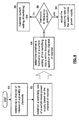
- FIG. 4 is a logic diagram of a method for mitigating interference with a switch mode power supply that begins at Step 50 .
- a channel of interest is compared with a switching rate of a switch mode power supply.
- the channel of interest is one of a plurality of channels such as FM radio channels wherein the corresponding carrier frequency is compared with the switching rate of the switch mode power supply.
- the process then proceeds to Step 52 where a determination is made as to whether the comparison of Step 50 is favorable. If the comparison is favorable, the process proceeds to Step 54 where the switching rate of the switch mode power supply is maintained.
- Step 56 the switching rate of the switch mode power supply is adjusted.
- the switching rate may be adjusted by adjusting a clock from which the switching rate is derived. The adjustment of the clock may be done with digital circuitry or software code that implements a logic function or a lookup table.
- the switching rate may be programmed based on the channel of interest such that once the channel of interest is known, the switching rate is programmed to a switching rate that does not produce an interfering harmonic.
- the switching rate may be incrementally adjusted and Steps 50 , 52 and 56 are repeated until a favorable comparison is achieved.
- FIG. 5 illustrates a logic diagram of another method for mitigating interference from a switch mode power supply.
- the process begins at Step 60 where a signal quality (e.g., signal to noise ratio (SNR), signal to interference ratio (SIR), received signal strength indication (RSSI), etc.) of the channel of interest is compared with a signal quality threshold.
- the process then proceeds to Step 62 where a determination is made as to whether the comparison at Step 60 was favorable (e.g., the SNR exceeds a threshold (e.g., 40 dB), the SIR exceeds a threshold (e.g., 40 dB), and/or the RSSI exceeds a threshold). If yes, the process proceeds to Step 64 where the switching rate of the switch mode power supply is maintained.
- the signal quality of the received signal is at such a level where the interference that may be produced by the switch mode power supply or a harmonic thereof, is negligible in comparison to the signal strength of the received signal.
- Step 66 a frequency spectrum of the channel of interest is determined.
- the frequency spectrum of the channel of interest corresponds to the bandwidth of the receiver tuned to receive the selected channel of interest.
- the frequency spectrum may be determined utilizing a lookup table or logical function implemented in either digital gates or software code.
- Step 68 a determination is made as to whether a harmonic of the switching rate of the switch mode power supply is within the frequency spectrum of the channel of interest. If, at Step 70 , the harmonic is not within the frequency spectrum, the process proceeds to Step 64 where the switching rate is maintained. If, however, the harmonic is within the frequency spectrum, the process proceeds to Step 72 where the switching rate of the switch mode power supply is adjusted.
- FIG. 6 is a logic diagram of another method for mitigating interference from a switch mode power supply.
- the process begins at Step 80 where a channel of interest of a plurality of channels is determined.
- the plurality of channels corresponds to a plurality of FM radio stations.
- the process then proceeds to Step 82 where a switching rate of a switch mode power supply is established based on the channel of interest. This may be done as shown in Steps 84 - 90 .
- Step 84 a determination is made as to whether a harmonic of a current setting of the switching rate of the switch mode power supply is within a frequency spectrum of the channel of interest. The process then proceeds to Step 86 where the method branches based on whether the harmonic is within the frequency spectrum. If not, the process proceeds to Step 88 where the current setting of the switching rate is maintained. If, however, the harmonic is within the frequency spectrum, the process proceeds to Step 90 where the switching rate of the switch mode power supply is adjusted.
- the term “substantially” or “approximately”, as may be used herein, provides an industry-accepted tolerance to its corresponding term and/or relativity between items. Such an industry-accepted tolerance ranges from less than one percent to twenty percent and corresponds to, but is not limited to, component values, integrated circuit process variations, temperature variations, rise and fall times, and/or thermal noise. Such relativity between items ranges from a difference of a few percent to magnitude differences.
- operably coupled includes direct coupling and indirect coupling via another component, element, circuit, or module where, for indirect coupling, the intervening component, element, circuit, or module does not modify the information of a signal but may adjust its current level, voltage level, and/or power level.
- inferred coupling i.e., where one element is coupled to another element by inference
- inferred coupling includes direct and indirect coupling between two elements in the same manner as “operably coupled”.
- the term “operably associated with”, as may be used herein, includes direct and/or indirect coupling of separate components and/or one component being embedded within another component.
- the term “compares favorably”, as may be used herein, indicates that a comparison between two or more elements, items, signals, etc., provides a desired relationship. For example, when the desired relationship is that signal 1 has a greater magnitude than signal 2 , a favorable comparison may be achieved when the magnitude of signal 1 is greater than that of signal 2 or when the magnitude of signal 2 is less than that of signal 1 .
- transistors in the above described figure(s) is/are shown as field effect transistors (FETs), as one of ordinary skill in the art will appreciate, the transistors may be implemented using any type of transistor structure including, but not limited to, bipolar, metal oxide semiconductor field effect transistors (MOSFET), N-well transistors, P-well transistors, enhancement mode, depletion mode, and zero voltage threshold (VT) transistors.
- FETs field effect transistors
- MOSFET metal oxide semiconductor field effect transistors
- N-well transistors N-well transistors
- P-well transistors P-well transistors
- enhancement mode enhancement mode
- depletion mode depletion mode
- VT zero voltage threshold
Landscapes
- Engineering & Computer Science (AREA)
- Computer Networks & Wireless Communication (AREA)
- Signal Processing (AREA)
- Noise Elimination (AREA)
Abstract
Description
Claims (18)
Priority Applications (1)
| Application Number | Priority Date | Filing Date | Title |
|---|---|---|---|
| US11/355,477 US7720456B2 (en) | 2006-02-16 | 2006-02-16 | Adjust switching rate of a power supply to mitigate interference |
Applications Claiming Priority (1)
| Application Number | Priority Date | Filing Date | Title |
|---|---|---|---|
| US11/355,477 US7720456B2 (en) | 2006-02-16 | 2006-02-16 | Adjust switching rate of a power supply to mitigate interference |
Publications (2)
| Publication Number | Publication Date |
|---|---|
| US20070191073A1 US20070191073A1 (en) | 2007-08-16 |
| US7720456B2 true US7720456B2 (en) | 2010-05-18 |
Family
ID=38369317
Family Applications (1)
| Application Number | Title | Priority Date | Filing Date |
|---|---|---|---|
| US11/355,477 Active 2027-06-12 US7720456B2 (en) | 2006-02-16 | 2006-02-16 | Adjust switching rate of a power supply to mitigate interference |
Country Status (1)
| Country | Link |
|---|---|
| US (1) | US7720456B2 (en) |
Families Citing this family (10)
| Publication number | Priority date | Publication date | Assignee | Title |
|---|---|---|---|---|
| WO2006065303A2 (en) * | 2004-12-16 | 2006-06-22 | Intellectual Solutions, Inc. | Combined modulator and digital file player having socket power supply adapter and/or universal connector |
| WO2007103857A2 (en) * | 2006-03-03 | 2007-09-13 | Intellectual Solutions, Inc. | Combined modulator and inverter |
| KR101212093B1 (en) * | 2006-11-01 | 2012-12-13 | 삼성전자주식회사 | Signal receiving apparatus and signal power prediction method thereof |
| US8145149B2 (en) * | 2010-06-17 | 2012-03-27 | R2 Semiconductor, Inc | Operating a voltage regulator at a switching frequency selected to reduce spurious signals |
| DE102011003559A1 (en) * | 2011-02-03 | 2012-08-09 | Robert Bosch Gmbh | Method and device for controlling a pulse inverter, which serves to control an electrical machine |
| US9059642B2 (en) * | 2012-08-22 | 2015-06-16 | Atmel Corporation | Digitally controlled spur management technique for integrated DC-DC converters |
| US9304625B2 (en) | 2013-06-28 | 2016-04-05 | Synaptics Incorporated | Synchronizing a switched power supply |
| US9014637B1 (en) * | 2013-09-27 | 2015-04-21 | Intel Corporation | Dynamic switching frequency control of an on-chip or integrated voltage regulator |
| US9209911B2 (en) | 2013-10-25 | 2015-12-08 | Kam Chow Cheung | Radio with a switched mode power supply |
| US12308803B2 (en) * | 2022-08-24 | 2025-05-20 | Shenzhen Jiangnan Industrial Co., Ltd. | Switching power supply frequency adaptive adjustment method, system and electronic device |
Citations (11)
| Publication number | Priority date | Publication date | Assignee | Title |
|---|---|---|---|---|
| US5079410A (en) * | 1991-01-25 | 1992-01-07 | General Electric Company | Power control system adaptable to a plurality of supply voltages |
| US5519889A (en) * | 1994-02-04 | 1996-05-21 | Ford Motor Company | Method and apparatus to conceal RF interference in AM radio reception caused by a switch mode power supply |
| US6505035B2 (en) * | 1998-04-17 | 2003-01-07 | Matsushita Electric Industrial Co., Ltd. | Radio communication apparatus and transmission rate control method |
| US20040085933A1 (en) * | 2002-11-04 | 2004-05-06 | Tia Mobile, Inc. | Satellite antenna system employing electronic elevation control for signal acquisition and tracking |
| US6819912B2 (en) * | 2001-11-05 | 2004-11-16 | Freescale Semiconductor, Inc. | Variable frequency switching amplifier and method therefor |
| US20050003773A1 (en) * | 2003-06-07 | 2005-01-06 | Cowley Nicholas Paul | Multiple conversion tuner |
| US7142819B1 (en) * | 2000-08-30 | 2006-11-28 | Cirrus Logic, Inc. | Circuits and methods for controlling switching noise in switched-mode circuits |
| US7197290B2 (en) * | 2003-09-18 | 2007-03-27 | General Motors Corporation | Method for AM band interference suppression via frequency shift |
| US7206563B1 (en) * | 2003-04-17 | 2007-04-17 | Apogee Technology, Inc. | Reduction of radio frequency interference (RFI) produced by switching amplifiers |
| US7457604B2 (en) * | 2003-09-18 | 2008-11-25 | General Motors Corporation | Method for suppressing motor vehicle radio interference |
| US7599676B2 (en) * | 2007-01-31 | 2009-10-06 | Silicon Laboratories, Inc. | Power consumption reduction techniques for an RF receiver implementing a mixing DAC architecture |
-
2006
- 2006-02-16 US US11/355,477 patent/US7720456B2/en active Active
Patent Citations (11)
| Publication number | Priority date | Publication date | Assignee | Title |
|---|---|---|---|---|
| US5079410A (en) * | 1991-01-25 | 1992-01-07 | General Electric Company | Power control system adaptable to a plurality of supply voltages |
| US5519889A (en) * | 1994-02-04 | 1996-05-21 | Ford Motor Company | Method and apparatus to conceal RF interference in AM radio reception caused by a switch mode power supply |
| US6505035B2 (en) * | 1998-04-17 | 2003-01-07 | Matsushita Electric Industrial Co., Ltd. | Radio communication apparatus and transmission rate control method |
| US7142819B1 (en) * | 2000-08-30 | 2006-11-28 | Cirrus Logic, Inc. | Circuits and methods for controlling switching noise in switched-mode circuits |
| US6819912B2 (en) * | 2001-11-05 | 2004-11-16 | Freescale Semiconductor, Inc. | Variable frequency switching amplifier and method therefor |
| US20040085933A1 (en) * | 2002-11-04 | 2004-05-06 | Tia Mobile, Inc. | Satellite antenna system employing electronic elevation control for signal acquisition and tracking |
| US7206563B1 (en) * | 2003-04-17 | 2007-04-17 | Apogee Technology, Inc. | Reduction of radio frequency interference (RFI) produced by switching amplifiers |
| US20050003773A1 (en) * | 2003-06-07 | 2005-01-06 | Cowley Nicholas Paul | Multiple conversion tuner |
| US7197290B2 (en) * | 2003-09-18 | 2007-03-27 | General Motors Corporation | Method for AM band interference suppression via frequency shift |
| US7457604B2 (en) * | 2003-09-18 | 2008-11-25 | General Motors Corporation | Method for suppressing motor vehicle radio interference |
| US7599676B2 (en) * | 2007-01-31 | 2009-10-06 | Silicon Laboratories, Inc. | Power consumption reduction techniques for an RF receiver implementing a mixing DAC architecture |
Also Published As
| Publication number | Publication date |
|---|---|
| US20070191073A1 (en) | 2007-08-16 |
Similar Documents
| Publication | Publication Date | Title |
|---|---|---|
| US11005368B2 (en) | Hysteretic window adjustment of tri-level switching regulator | |
| US5559471A (en) | Amplifier and biasing circuit therefor | |
| US7564922B2 (en) | RF transmitter for efficiently compensating output power variation due to temperature and process | |
| US8760222B2 (en) | Method and apparatus for controlling or managing bandwidth of a filter circuit within a system having two integrated circuits | |
| US7728668B2 (en) | Variable-gain amplification circuit, receiver and receiver IC | |
| CN101228720B (en) | Dual voltage regulator for a supply voltage controlled power amplifier in a closed power control loop | |
| US8073416B2 (en) | Method and apparatus for controlling a bias current of a VCO in a phase-locked loop | |
| US8140027B2 (en) | Automatic frequency tuning system and method for an FM-band transmit power amplifier | |
| US20050231297A1 (en) | Temperature stabilized voltage controlled oscillator | |
| CN103314524B (en) | Adjustment duty ratio is to improve the efficiency of digital radio frequency power amplifier | |
| US7720456B2 (en) | Adjust switching rate of a power supply to mitigate interference | |
| US8525595B2 (en) | Vramp limiting using resistors | |
| JP2017517073A (en) | On-chip dual supply multimode CMOS regulator | |
| GB2428313A (en) | Voltage controlled oscillator with automatic amplitude control | |
| US8736249B2 (en) | High frequency power detector circuit and radio communication device | |
| Shibata et al. | A 22nm 0.84 mm 2 BLE transceiver with self IQ-phase correction achieving 39dB image rejection and on-chip antenna impedance tuning | |
| WO2020024919A1 (en) | Dual mode power supply for voltage controlled oscillators | |
| US20110053537A1 (en) | Frequency modulation receiver with a low power frequency synthesizer | |
| US9094021B2 (en) | Semiconductor device and variation information obtaining program | |
| WO2015057700A1 (en) | Dynamic bias to improve switch linearity | |
| Peng et al. | A coin-battery-powered LDO-free 2.4-GHz Bluetooth low-energy transmitter with 34.7% peak system efficiency | |
| US20210046320A1 (en) | Voltage converting device | |
| US7312655B2 (en) | Apparatus and method for controlling bias adaptation bias of a high power amplifier | |
| US7933369B2 (en) | Apparatus for automatic gain control and wireless receiver employing the same | |
| US9503136B2 (en) | Receiver and receiving method of receiver |
Legal Events
| Date | Code | Title | Description |
|---|---|---|---|
| AS | Assignment |
Owner name: SIGMATEL, INC.,TEXAS Free format text: ASSIGNMENT OF ASSIGNORS INTEREST;ASSIGNORS:MAY, MICHAEL R.;MAY, MARCUS W.;HENSON, MATTHEW BRADY;REEL/FRAME:017597/0216 Effective date: 20060215 Owner name: SIGMATEL, INC., TEXAS Free format text: ASSIGNMENT OF ASSIGNORS INTEREST;ASSIGNORS:MAY, MICHAEL R.;MAY, MARCUS W.;HENSON, MATTHEW BRADY;REEL/FRAME:017597/0216 Effective date: 20060215 |
|
| AS | Assignment |
Owner name: CITIBANK, N.A.,NEW YORK Free format text: SECURITY AGREEMENT;ASSIGNOR:SIGMATEL, INC.;REEL/FRAME:021212/0372 Effective date: 20080605 Owner name: CITIBANK, N.A., NEW YORK Free format text: SECURITY AGREEMENT;ASSIGNOR:SIGMATEL, INC.;REEL/FRAME:021212/0372 Effective date: 20080605 |
|
| FEPP | Fee payment procedure |
Free format text: PAYOR NUMBER ASSIGNED (ORIGINAL EVENT CODE: ASPN); ENTITY STATUS OF PATENT OWNER: LARGE ENTITY |
|
| AS | Assignment |
Owner name: CITIBANK, N.A., NEW YORK Free format text: SECURITY AGREEMENT;ASSIGNOR:FREESCALE SEMICONDUCTOR, INC.;REEL/FRAME:024085/0001 Effective date: 20100219 Owner name: CITIBANK, N.A.,NEW YORK Free format text: SECURITY AGREEMENT;ASSIGNOR:FREESCALE SEMICONDUCTOR, INC.;REEL/FRAME:024085/0001 Effective date: 20100219 |
|
| AS | Assignment |
Owner name: CITIBANK, N.A., NEW YORK Free format text: SECURITY AGREEMENT;ASSIGNOR:SIGMATEL, LLC;REEL/FRAME:024079/0406 Effective date: 20100219 Owner name: CITIBANK, N.A.,NEW YORK Free format text: SECURITY AGREEMENT;ASSIGNOR:SIGMATEL, LLC;REEL/FRAME:024079/0406 Effective date: 20100219 |
|
| STCF | Information on status: patent grant |
Free format text: PATENTED CASE |
|
| AS | Assignment |
Owner name: CITIBANK, N.A., AS NOTES COLLATERAL AGENT, NEW YOR Free format text: SECURITY AGREEMENT;ASSIGNOR:SIGMATEL, LLC;REEL/FRAME:024358/0439 Effective date: 20100413 Owner name: CITIBANK, N.A., AS NOTES COLLATERAL AGENT,NEW YORK Free format text: SECURITY AGREEMENT;ASSIGNOR:SIGMATEL, LLC;REEL/FRAME:024358/0439 Effective date: 20100413 |
|
| AS | Assignment |
Owner name: CITIBANK, N.A., AS COLLATERAL AGENT, NEW YORK Free format text: SECURITY AGREEMENT;ASSIGNOR:FREESCALE SEMICONDUCTOR, INC.;REEL/FRAME:024397/0001 Effective date: 20100413 Owner name: CITIBANK, N.A., AS COLLATERAL AGENT,NEW YORK Free format text: SECURITY AGREEMENT;ASSIGNOR:FREESCALE SEMICONDUCTOR, INC.;REEL/FRAME:024397/0001 Effective date: 20100413 |
|
| CC | Certificate of correction | ||
| AS | Assignment |
Owner name: CITIBANK, N.A., AS NOTES COLLATERAL AGENT, NEW YOR Free format text: SECURITY AGREEMENT;ASSIGNOR:SIGMATEL, LLC;REEL/FRAME:030628/0636 Effective date: 20130521 |
|
| AS | Assignment |
Owner name: CITIBANK, N.A., AS NOTES COLLATERAL AGENT, NEW YOR Free format text: SECURITY AGREEMENT;ASSIGNOR:SIGMATEL, LLC;REEL/FRAME:031626/0218 Effective date: 20131101 |
|
| FPAY | Fee payment |
Year of fee payment: 4 |
|
| AS | Assignment |
Owner name: SIGMATEL, INC., TEXAS Free format text: PATENT RELEASE;ASSIGNOR:CITIBANK, N.A., AS COLLATERAL AGENT;REEL/FRAME:037355/0838 Effective date: 20151207 Owner name: SIGMATEL, INC., TEXAS Free format text: PATENT RELEASE;ASSIGNOR:CITIBANK, N.A., AS COLLATERAL AGENT;REEL/FRAME:037354/0773 Effective date: 20151207 Owner name: FREESCALE SEMICONDUCTOR, INC., TEXAS Free format text: PATENT RELEASE;ASSIGNOR:CITIBANK, N.A., AS COLLATERAL AGENT;REEL/FRAME:037356/0143 Effective date: 20151207 Owner name: SIGMATEL, INC., TEXAS Free format text: PATENT RELEASE;ASSIGNOR:CITIBANK, N.A., AS COLLATERAL AGENT;REEL/FRAME:037354/0734 Effective date: 20151207 Owner name: FREESCALE SEMICONDUCTOR, INC., TEXAS Free format text: PATENT RELEASE;ASSIGNOR:CITIBANK, N.A., AS COLLATERAL AGENT;REEL/FRAME:037356/0553 Effective date: 20151207 |
|
| AS | Assignment |
Owner name: SIGMATEL, LLC, TEXAS Free format text: CORRECTIVE ASSIGNMENT TO CORRECT THE ASSIGNEE NAME PREVIOUSLY RECORDED AT REEL: 037354 FRAME: 0773. ASSIGNOR(S) HEREBY CONFIRMS THE PATENT RELEASE;ASSIGNOR:CITIBANK, N.A., AS COLLATERAL AGENT;REEL/FRAME:039723/0777 Effective date: 20151207 |
|
| AS | Assignment |
Owner name: NXP USA, INC., TEXAS Free format text: MERGER;ASSIGNOR:SIGMATEL, LLC;REEL/FRAME:043328/0351 Effective date: 20170718 |
|
| AS | Assignment |
Owner name: SIGMATEL, LLC, DELAWARE Free format text: CHANGE OF NAME;ASSIGNOR:SIGMATEL, INC.;REEL/FRAME:043735/0306 Effective date: 20090101 |
|
| MAFP | Maintenance fee payment |
Free format text: PAYMENT OF MAINTENANCE FEE, 8TH YEAR, LARGE ENTITY (ORIGINAL EVENT CODE: M1552) Year of fee payment: 8 |
|
| MAFP | Maintenance fee payment |
Free format text: PAYMENT OF MAINTENANCE FEE, 12TH YEAR, LARGE ENTITY (ORIGINAL EVENT CODE: M1553); ENTITY STATUS OF PATENT OWNER: LARGE ENTITY Year of fee payment: 12 |