US7679387B2 - Inspection method, inspection apparatus, and control program for performing electrical inspection by using probe - Google Patents
Inspection method, inspection apparatus, and control program for performing electrical inspection by using probe Download PDFInfo
- Publication number
- US7679387B2 US7679387B2 US12/279,864 US27986407A US7679387B2 US 7679387 B2 US7679387 B2 US 7679387B2 US 27986407 A US27986407 A US 27986407A US 7679387 B2 US7679387 B2 US 7679387B2
- Authority
- US
- United States
- Prior art keywords
- probe
- electrode
- fritting
- inspection
- electrical
- Prior art date
- Legal status (The legal status is an assumption and is not a legal conclusion. Google has not performed a legal analysis and makes no representation as to the accuracy of the status listed.)
- Expired - Fee Related
Links
Images


Classifications
-
- G—PHYSICS
- G01—MEASURING; TESTING
- G01R—MEASURING ELECTRIC VARIABLES; MEASURING MAGNETIC VARIABLES
- G01R1/00—Details of instruments or arrangements of the types included in groups G01R5/00 - G01R13/00 and G01R31/00
- G01R1/02—General constructional details
- G01R1/06—Measuring leads; Measuring probes
- G01R1/067—Measuring probes
-
- G—PHYSICS
- G01—MEASURING; TESTING
- G01R—MEASURING ELECTRIC VARIABLES; MEASURING MAGNETIC VARIABLES
- G01R31/00—Arrangements for testing electric properties; Arrangements for locating electric faults; Arrangements for electrical testing characterised by what is being tested not provided for elsewhere
- G01R31/28—Testing of electronic circuits, e.g. by signal tracer
- G01R31/2851—Testing of integrated circuits [IC]
- G01R31/2886—Features relating to contacting the IC under test, e.g. probe heads; chucks
- G01R31/2891—Features relating to contacting the IC under test, e.g. probe heads; chucks related to sensing or controlling of force, position, temperature
-
- H10P74/00—
Definitions
- the present invention provides an inspection method, an inspection apparatus and a control program, capable of accurately and reliably performing an inspection by obtaining a good electrical contact state more securely in comparison with the conventional method.
- an inspection method for performing an electrical inspection by bringing a probe into contact with an electrode of a target object to be inspected including: a process of reducing an electrical resistance value between the electrode and the probe to a first predetermined value or less by bringing the probe into contact with the electrode at a predetermined load so as to apply a mechanical damage to an insulating film on the electrode; and a fritting process of reducing the electrical resistance value between the electrode and the probe to a second predetermined value or less which is smaller than the first predetermined value by applying an electrical damage to the insulating film on the electrode by means of a fritting phenomenon.
- a control program for controlling an inspection apparatus which performs an electrical inspection by bringing a probe into contact with an electrode of a target object to be inspected, the program including the steps of: reducing an electrical resistance value between the electrode and the probe to a first predetermined value or less by bringing the probe into contact with the electrode at a predetermined load so as to apply a mechanical damage to an insulating film on the electrode; reducing the electrical resistance value between the electrode and the probe to a second predetermined value or less which is smaller than the first predetermined value by applying an electrical damage to the insulating film on the electrode by means of a fritting phenomenon; and performing the electrical inspection of the target object to be inspected.
- the first predetermined value is 1 M ⁇ , and the predetermined load is 1 g or less.
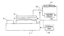
- FIG. 1 is a schematic configuration view of principal parts of a probe apparatus in accordance with an embodiment of the present invention
- a fritting phenomenon refers to a phenomenon in which, when a potential gradient applied to an insulating film such as an oxide film and the like formed on a surface of a metal (an electrode in the present embodiment) becomes about 10 5 to 10 6 V/cm, an electric current flows due to a non-uniformity in a thickness of the insulating film or a composition of the metal, thereby breaking down the insulating film.
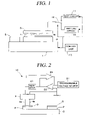
- FIG. 2 shows a schematic configuration view of the fritting circuit 10 for incurring such fritting phenomenon.
- the fritting circuit 10 includes a programmable voltage source 21 , a voltage application buffer amplifier 22 , a current sense resistor 23 and an application current limiter 24 .
- the fritting circuit 10 is configured so that a voltage is applied to probes 4 a and 4 b of the probe card 3 from the programmable voltage source 21 .
- the probe 4 a is connected to the voltage application buffer amplifier 22 via the current sense resistor 23 . Further, the probe 4 b is connected to an input terminal side of the voltage application buffer amplifier 22 while being grounded.
- the probes 4 a and 4 b are made of, for example, a conductive metal such as tungsten (W), beryllium copper alloy (BeCu), palladium (Pd) or the like. Furthermore, a diameter of leading ends of the probes 4 a and 4 b is selected according to a size of an electrode of an target object, and thus, if the target object is an semiconductor device, the diameter is, for example, about 20 ⁇ m.
- the probe 4 a is for inspecting, and it can be used in an electrical inspection by the test circuit 11 as well as in a fritting by the fritting circuit 10 .
- the other probe 4 b is for fritting by the fritting circuit 10 , and when performing the electrical inspection by the test circuit 11 , it becomes an electrically floating state.
- the leading end portions of the probes 4 a and 4 b are pressed against the polishing unit 5 at a predetermined load by driving the driving table 1 , and in this state, the driving table 1 is moved in a horizontal direction. While the leading end portions of the probes 4 a and 4 b are in contact with the polishing unit 5 , the polishing unit 5 slides to polish the leading end portions, thereby forming irregularities by making the surface state thereof rough.
- the voltage is applied to the probe 4 a via the voltage application buffer amplifier 22 and the current sense resistor 23 , a very little amount of tunneling current flows at first if the insulating film O is very thin. From this state, if the voltage of the programmable voltage source 21 is gradually raised, the potential gradient between the probes 4 a and 4 b gradually becomes large. When the potential gradient reaches a predetermined value (about 10 5 to 10 6 V/cm), the fritting phenomenon occurs, resulting in the breakdown of the insulating film O on the electrode P. Accordingly, the probes 4 a and 4 b are brought into contact with a metal surface of the electrode P, and an electric current between the probe 4 a and the probe 4 b becomes large rapidly.
- a predetermined value about 10 5 to 10 6 V/cm
Landscapes
- Engineering & Computer Science (AREA)
- Physics & Mathematics (AREA)
- General Physics & Mathematics (AREA)
- Computer Hardware Design (AREA)
- Microelectronics & Electronic Packaging (AREA)
- General Engineering & Computer Science (AREA)
- Testing Or Measuring Of Semiconductors Or The Like (AREA)
- Testing Of Individual Semiconductor Devices (AREA)
- Measuring Leads Or Probes (AREA)
- Tests Of Electronic Circuits (AREA)
Abstract
Description
Claims (13)
Applications Claiming Priority (3)
| Application Number | Priority Date | Filing Date | Title |
|---|---|---|---|
| JP2006-048024 | 2006-02-24 | ||
| JP2006048024A JP5108238B2 (en) | 2006-02-24 | 2006-02-24 | Inspection method, inspection apparatus, and control program |
| PCT/JP2007/052318 WO2007097207A1 (en) | 2006-02-24 | 2007-02-09 | Inspecting method, inspecting apparatus and control program |
Publications (2)
| Publication Number | Publication Date |
|---|---|
| US20090002008A1 US20090002008A1 (en) | 2009-01-01 |
| US7679387B2 true US7679387B2 (en) | 2010-03-16 |
Family
ID=38437247
Family Applications (1)
| Application Number | Title | Priority Date | Filing Date |
|---|---|---|---|
| US12/279,864 Expired - Fee Related US7679387B2 (en) | 2006-02-24 | 2007-02-09 | Inspection method, inspection apparatus, and control program for performing electrical inspection by using probe |
Country Status (5)
| Country | Link |
|---|---|
| US (1) | US7679387B2 (en) |
| JP (1) | JP5108238B2 (en) |
| KR (1) | KR101019238B1 (en) |
| TW (1) | TW200802663A (en) |
| WO (1) | WO2007097207A1 (en) |
Citations (3)
| Publication number | Priority date | Publication date | Assignee | Title |
|---|---|---|---|---|
| US6777967B2 (en) * | 2000-08-21 | 2004-08-17 | Tokyo Electron Limited | Inspection method and inspection apparatus |
| US20070063725A1 (en) * | 2003-06-09 | 2007-03-22 | Tokyo Electron Limited. | Inspection method and inspection apparatus for inspecting electrical characteristics of inspection object |
| US7301357B2 (en) * | 2002-12-12 | 2007-11-27 | Tokyo Electron Limited | Inspection method and inspection equipment |
Family Cites Families (4)
| Publication number | Priority date | Publication date | Assignee | Title |
|---|---|---|---|---|
| JP2002071718A (en) * | 2000-08-25 | 2002-03-12 | Hitachi Ltd | Semiconductor inspection apparatus and semiconductor device manufacturing method |
| JP2004093451A (en) * | 2002-09-02 | 2004-03-25 | Tokyo Electron Ltd | Probe method and probe device |
| JP2005037199A (en) * | 2003-07-18 | 2005-02-10 | Yamaha Corp | Probe unit, the continuity test method, and its manufacturing method |
| US20090128171A1 (en) * | 2005-03-31 | 2009-05-21 | Katsuya Okumura | Microstructure Probe Card, and Microstructure Inspecting Device, Method, and Computer Program |
-
2006
- 2006-02-24 JP JP2006048024A patent/JP5108238B2/en not_active Expired - Fee Related
-
2007
- 2007-02-09 US US12/279,864 patent/US7679387B2/en not_active Expired - Fee Related
- 2007-02-09 WO PCT/JP2007/052318 patent/WO2007097207A1/en not_active Ceased
- 2007-02-09 KR KR1020087019820A patent/KR101019238B1/en not_active Expired - Fee Related
- 2007-02-14 TW TW096105496A patent/TW200802663A/en not_active IP Right Cessation
Patent Citations (4)
| Publication number | Priority date | Publication date | Assignee | Title |
|---|---|---|---|---|
| US6777967B2 (en) * | 2000-08-21 | 2004-08-17 | Tokyo Electron Limited | Inspection method and inspection apparatus |
| US7301357B2 (en) * | 2002-12-12 | 2007-11-27 | Tokyo Electron Limited | Inspection method and inspection equipment |
| US20070063725A1 (en) * | 2003-06-09 | 2007-03-22 | Tokyo Electron Limited. | Inspection method and inspection apparatus for inspecting electrical characteristics of inspection object |
| US7262613B2 (en) * | 2003-06-09 | 2007-08-28 | Tokyo Electron Limited | Inspection method and inspection apparatus for inspecting electrical characteristics of inspection object |
Also Published As
| Publication number | Publication date |
|---|---|
| TW200802663A (en) | 2008-01-01 |
| JP5108238B2 (en) | 2012-12-26 |
| JP2007227714A (en) | 2007-09-06 |
| KR20080085224A (en) | 2008-09-23 |
| US20090002008A1 (en) | 2009-01-01 |
| TWI333679B (en) | 2010-11-21 |
| KR101019238B1 (en) | 2011-03-04 |
| WO2007097207A1 (en) | 2007-08-30 |
Similar Documents
| Publication | Publication Date | Title |
|---|---|---|
| US7319339B2 (en) | Inspection apparatus to break the oxide of an electrode by fritting phenomenon | |
| KR100965440B1 (en) | Computer-readable storage media storing test methods, test devices and programs | |
| KR100842784B1 (en) | Inspection method and inspection equipment | |
| US11169180B2 (en) | Method for producing probes for testing integrated electronic circuits | |
| US20080150559A1 (en) | Method for probing impact sensitve and thin layered substrate | |
| EP1788401A1 (en) | Method and apparatus for testing electrical characteristics of object under test | |
| US7679387B2 (en) | Inspection method, inspection apparatus, and control program for performing electrical inspection by using probe | |
| JP3061619B1 (en) | How to measure probe contact resistance | |
| JP2007285882A (en) | Board inspection contact, tool, and system | |
| JP2008261678A (en) | Inspection probe contact detection mechanism and circuit board inspection device | |
| JP2003234384A (en) | Probing apparatus of grinding and contact check integrated type, and grinding method thereof | |
| US9535114B2 (en) | Testing device | |
| US20100039130A1 (en) | Inspecting method, inspecting apparatus and computer readable storage medium having program stored therein | |
| JP6647811B2 (en) | Electrical connection device and inspection method | |
| JP5179276B2 (en) | Circuit board inspection equipment | |
| JP2002217255A (en) | Semiconductor measuring equipment | |
| TWI640781B (en) | Inspection probe, inspection fixture, and manufacturing method for inspection probe |
Legal Events
| Date | Code | Title | Description |
|---|---|---|---|
| AS | Assignment |
Owner name: TOKYO ELECTRON LIMITED, JAPAN Free format text: ASSIGNMENT OF ASSIGNORS INTEREST;ASSIGNOR:HYAKUDOMI, TAKANORI;REEL/FRAME:021407/0054 Effective date: 20080731 Owner name: TOKYO ELECTRON LIMITED,JAPAN Free format text: ASSIGNMENT OF ASSIGNORS INTEREST;ASSIGNOR:HYAKUDOMI, TAKANORI;REEL/FRAME:021407/0054 Effective date: 20080731 |
|
| FEPP | Fee payment procedure |
Free format text: PAYOR NUMBER ASSIGNED (ORIGINAL EVENT CODE: ASPN); ENTITY STATUS OF PATENT OWNER: LARGE ENTITY |
|
| FPAY | Fee payment |
Year of fee payment: 4 |
|
| FEPP | Fee payment procedure |
Free format text: MAINTENANCE FEE REMINDER MAILED (ORIGINAL EVENT CODE: REM.) |
|
| LAPS | Lapse for failure to pay maintenance fees |
Free format text: PATENT EXPIRED FOR FAILURE TO PAY MAINTENANCE FEES (ORIGINAL EVENT CODE: EXP.) |
|
| STCH | Information on status: patent discontinuation |
Free format text: PATENT EXPIRED DUE TO NONPAYMENT OF MAINTENANCE FEES UNDER 37 CFR 1.362 |
|
| FP | Lapsed due to failure to pay maintenance fee |
Effective date: 20180316 |