US7673519B1 - Pressure sensor featuring offset cancellation and method of making - Google Patents
Pressure sensor featuring offset cancellation and method of making Download PDFInfo
- Publication number
- US7673519B1 US7673519B1 US12/201,211 US20121108A US7673519B1 US 7673519 B1 US7673519 B1 US 7673519B1 US 20121108 A US20121108 A US 20121108A US 7673519 B1 US7673519 B1 US 7673519B1
- Authority
- US
- United States
- Prior art keywords
- electrodes
- portions
- common electrode
- geometry
- sense
- Prior art date
- Legal status (The legal status is an assumption and is not a legal conclusion. Google has not performed a legal analysis and makes no representation as to the accuracy of the status listed.)
- Expired - Fee Related, expires
Links
- 238000004519 manufacturing process Methods 0.000 title claims description 6
- 239000012528 membrane Substances 0.000 claims abstract description 75
- 239000003990 capacitor Substances 0.000 claims abstract description 38
- 239000000758 substrate Substances 0.000 claims description 30
- 238000000034 method Methods 0.000 claims description 9
- 239000004065 semiconductor Substances 0.000 claims description 9
- 238000004873 anchoring Methods 0.000 claims description 2
- 239000000463 material Substances 0.000 description 13
- 238000000151 deposition Methods 0.000 description 11
- 238000002955 isolation Methods 0.000 description 10
- 229910021420 polycrystalline silicon Inorganic materials 0.000 description 10
- 229920005591 polysilicon Polymers 0.000 description 10
- 238000013461 design Methods 0.000 description 9
- 230000008021 deposition Effects 0.000 description 8
- 238000001514 detection method Methods 0.000 description 7
- 230000035945 sensitivity Effects 0.000 description 7
- 238000001465 metallisation Methods 0.000 description 6
- XUIMIQQOPSSXEZ-UHFFFAOYSA-N Silicon Chemical compound [Si] XUIMIQQOPSSXEZ-UHFFFAOYSA-N 0.000 description 4
- 238000000059 patterning Methods 0.000 description 4
- 230000004044 response Effects 0.000 description 4
- 229910052710 silicon Inorganic materials 0.000 description 4
- 239000010703 silicon Substances 0.000 description 4
- OAICVXFJPJFONN-UHFFFAOYSA-N Phosphorus Chemical compound [P] OAICVXFJPJFONN-UHFFFAOYSA-N 0.000 description 3
- 230000015572 biosynthetic process Effects 0.000 description 3
- 230000008859 change Effects 0.000 description 3
- 150000004767 nitrides Chemical class 0.000 description 3
- 238000002161 passivation Methods 0.000 description 3
- BOTDANWDWHJENH-UHFFFAOYSA-N Tetraethyl orthosilicate Chemical compound CCO[Si](OCC)(OCC)OCC BOTDANWDWHJENH-UHFFFAOYSA-N 0.000 description 2
- 230000008901 benefit Effects 0.000 description 2
- 230000008878 coupling Effects 0.000 description 2
- 238000010168 coupling process Methods 0.000 description 2
- 238000005859 coupling reaction Methods 0.000 description 2
- 239000002019 doping agent Substances 0.000 description 2
- 238000012986 modification Methods 0.000 description 2
- 230000004048 modification Effects 0.000 description 2
- 210000004457 myocytus nodalis Anatomy 0.000 description 2
- 230000008569 process Effects 0.000 description 2
- 238000012546 transfer Methods 0.000 description 2
- JBRZTFJDHDCESZ-UHFFFAOYSA-N AsGa Chemical compound [As]#[Ga] JBRZTFJDHDCESZ-UHFFFAOYSA-N 0.000 description 1
- 229910001218 Gallium arsenide Inorganic materials 0.000 description 1
- 229910000577 Silicon-germanium Inorganic materials 0.000 description 1
- LEVVHYCKPQWKOP-UHFFFAOYSA-N [Si].[Ge] Chemical compound [Si].[Ge] LEVVHYCKPQWKOP-UHFFFAOYSA-N 0.000 description 1
- CSDREXVUYHZDNP-UHFFFAOYSA-N alumanylidynesilicon Chemical compound [Al].[Si] CSDREXVUYHZDNP-UHFFFAOYSA-N 0.000 description 1
- 239000011248 coating agent Substances 0.000 description 1
- 238000000576 coating method Methods 0.000 description 1
- 238000012937 correction Methods 0.000 description 1
- 238000011161 development Methods 0.000 description 1
- 239000003989 dielectric material Substances 0.000 description 1
- 230000000694 effects Effects 0.000 description 1
- BHEPBYXIRTUNPN-UHFFFAOYSA-N hydridophosphorus(.) (triplet) Chemical compound [PH] BHEPBYXIRTUNPN-UHFFFAOYSA-N 0.000 description 1
- 239000012212 insulator Substances 0.000 description 1
- 229910021421 monocrystalline silicon Inorganic materials 0.000 description 1
- 230000003071 parasitic effect Effects 0.000 description 1
- 238000002360 preparation method Methods 0.000 description 1
- 238000012913 prioritisation Methods 0.000 description 1
- 238000012545 processing Methods 0.000 description 1
- 238000007789 sealing Methods 0.000 description 1
- 239000005368 silicate glass Substances 0.000 description 1
- 230000002277 temperature effect Effects 0.000 description 1
- 230000002123 temporal effect Effects 0.000 description 1
- 239000011800 void material Substances 0.000 description 1
Images


Classifications
-
- G—PHYSICS
- G01—MEASURING; TESTING
- G01L—MEASURING FORCE, STRESS, TORQUE, WORK, MECHANICAL POWER, MECHANICAL EFFICIENCY, OR FLUID PRESSURE
- G01L9/00—Measuring steady of quasi-steady pressure of fluid or fluent solid material by electric or magnetic pressure-sensitive elements; Transmitting or indicating the displacement of mechanical pressure-sensitive elements, used to measure the steady or quasi-steady pressure of a fluid or fluent solid material, by electric or magnetic means
- G01L9/0041—Transmitting or indicating the displacement of flexible diaphragms
- G01L9/0072—Transmitting or indicating the displacement of flexible diaphragms using variations in capacitance
- G01L9/0073—Transmitting or indicating the displacement of flexible diaphragms using variations in capacitance using a semiconductive diaphragm
-
- Y—GENERAL TAGGING OF NEW TECHNOLOGICAL DEVELOPMENTS; GENERAL TAGGING OF CROSS-SECTIONAL TECHNOLOGIES SPANNING OVER SEVERAL SECTIONS OF THE IPC; TECHNICAL SUBJECTS COVERED BY FORMER USPC CROSS-REFERENCE ART COLLECTIONS [XRACs] AND DIGESTS
- Y10—TECHNICAL SUBJECTS COVERED BY FORMER USPC
- Y10T—TECHNICAL SUBJECTS COVERED BY FORMER US CLASSIFICATION
- Y10T29/00—Metal working
- Y10T29/49—Method of mechanical manufacture
- Y10T29/49002—Electrical device making
Definitions
- This disclosure relates generally to pressure sensors, and more specifically, to a pressure sensor featuring offset cancellation and a method of making the same.
- Leak detection and leak signal compensation are important features for micro-electromechanical systems MEMS pressure sensors, especially in automotive safety applications.
- a pressure leak in a MEMS pressure sensor may occur, for example, in response to a cracked membrane.
- time to market considerations foster a need for better re-use options between inertial (e.g., gyroscope, accelerometer, etc.) and pressure sensors.
- inertial e.g., gyroscope, accelerometer, etc.
- ASIC application specific integrated circuit
- FIG. 1 is a layout top view of a MEMS pressure sensor featuring offset cancellation according to one embodiment of the present disclosure
- FIG. 2 is a layout top view of the MEMS pressure sensor featuring offset cancellation of FIG. 1 , further showing cross-section references, according to one embodiment of the present disclosure
- FIG. 3 is a cross-section view of the MEMS pressure sensor featuring offset cancellation of FIG. 2 , taken along line 3 - 3 of FIG. 2 , according to one embodiment of the present disclosure;
- FIGS. 4-13 are cross-section views of the MEMS pressure sensor featuring offset cancellation of FIG. 2 , taken along line 4 - 4 of FIG. 2 , at different stages of manufacture, according to one embodiment of the present disclosure;
- FIG. 14 is a cross-section view of a MEMS pressure sensor featuring offset cancellation, similar to the embodiment of FIG. 2 taken along line 3 - 3 of FIG. 2 , according to another embodiment of the present disclosure;
- FIG. 15 is a cross-section view of a MEMS pressure sensor featuring offset cancellation, similar to the embodiment of FIG. 2 taken along line 3 - 3 of FIG. 2 , according to yet another embodiment of the present disclosure.
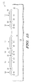
- FIG. 16 is a top-down view of a MEMS pressure sensor featuring offset cancellation, similar to the embodiment of FIG. 2 , according to still another embodiment of the present disclosure.
- a semiconductor substrate can be any semiconductor material or combinations of materials, such as gallium arsenide, silicon germanium, silicon-on-insulator (SOI), silicon, monocrystalline silicon, the like, and combinations of the above.
- SOI silicon-on-insulator
- the embodiments of the present disclosure are not limited to semiconductor substrates, but can include any suitable substrate for a given pressure sensor application.
- the pressure sensor architecture of the present disclosure advantageously reduces undesirable temperature effects and/or media effects.
- the embodiments further allow for development of next generation combo designs, including accelerometers and pressure sensor elements on a single die, while reducing cost, as the pressure sensor itself does not require a circuit on chip any more, but can advantageously re-use existing capacitance-to-voltage (C2V) circuitry on the ASIC side.
- C2V capacitance-to-voltage
- the embodiments of the present disclosure also advantageously provide offset cancellation for a dual-transducer pressure sensor.
- the embodiments further provide for improved leak detection.
- the MEMS pressure sensor includes at least the following aspects: (i) the MEMS pressure sensor design is substantially symmetric, (ii) the MEMS pressure sensor design has interleaved reference and sense elements, and (iii) the MEMS pressure sensor design has a common chamber (or cavity), wherein the chamber can include a vacuum chamber or a chamber filled with a suitable gas at a given controlled pressure.
- Any offset drift needs to match between the interleaved sensors, which is achieved by a substantially symmetric layout of poly runners and substantially identical bottom plates. In other words, matching of any offset drift between the interleaved sensors is achieved by a substantially symmetric layout of poly runners and substantially identical capacitor bottom electrode plates (as will be discussed further herein).
- the reference element of the MEMS pressure sensor design is created with a smaller diaphragm width than that of the sense element. Accordingly, this maintains a smallest possible die size and allows for better temperature coefficient (TC) cancellation, compared to increasing a thickness of a top capacitor electrode to create a corresponding reference element.
- TC temperature coefficient
- the MEMS pressure sensor transducer is designed to enable differential sensing of pressure and keep capacitive offset drifts substantially identical on both sides (i.e., on each of the sense and reference sides).
- the number of bottom capacitor electrodes can include four (4) electrodes, two (2) for the reference portion and two (2) for the sense portion of the pressure transducer. The particular number of bottom electrodes (or electrode plates) for reference and sense can be selected (or adjusted as necessary) according to the requirements of a given MEMS pressure sensor transducer implementation.
- FIG. 1 is a layout top view of a MEMS pressure sensor 10 featuring offset cancellation according to one embodiment of the present disclosure.
- MEMS pressure sensor 10 is fabricated on the surface of an insulative layer 12 .
- Insulative layer 12 can comprise any suitable insulative or dielectric material layer, selected according to the requirements of a given pressure sensor implementation.
- Electrodes 14 , 16 , 18 and 20 are formed overlying the surface of insulative layer 12 , wherein the electrodes are illustrated in phantom, due to the fact that they are beneath a common electrode 22 .
- Electrodes 16 and 20 represent a first set of sense capacitor bottom electrodes, while electrodes 14 and 18 represent a second set of reference capacitor bottom electrodes.
- the second set of electrodes ( 14 , 18 ) are configured in an interleaved arrangement with the first set of electrodes ( 16 , 20 ).
- a geometry of individual electrodes of the first set of electrodes ( 16 , 20 ) substantially matches a geometry of individual electrodes of the second set of electrodes ( 14 , 18 ), i.e., the geometries are substantially similar.
- the geometry of individual electrodes of the first set of electrodes matches the geometry of the individual electrodes of the second set of electrodes, i.e., the geometries are identical.
- the electrodes ( 16 , 20 ) of the first set of electrodes can each be characterized by a length dimension and a width dimension.
- the electrodes ( 14 , 18 ) of the second set of electrodes can also be characterized by a length dimension and a width dimension.
- the length and width dimensions of electrode 14 are represented by the dimension arrows 30 and 33 , respectively, in FIG. 1 .
- the length and width dimensions of electrode 16 are represented by the dimension arrows 30 and 35 , respectively, in FIG. 1 .
- the length and width dimensions of each of the electrodes ( 16 , 20 ) in the first set of electrodes equals the length and width dimensions of each of the electrodes ( 14 , 18 ) in the second set of electrodes.
- common electrode 22 represents a sense and reference capacitor top electrode.
- the top electrode 22 is (i) overlying, (ii) spaced from, and (iii) configured in connection with the first and second sets of electrodes, ( 16 , 20 ) and ( 14 , 18 ), respectively, to form a common vacuum cavity (as indicated by reference numeral 90 in FIG. 3 and to be discussed further herein).
- Common electrode 22 anchors to the surface of the insulative layer 12 for establishing (i) first portions corresponding to the sense membrane portions and (ii) second portions corresponding to the reference membrane portions. For example, in FIG.
- common electrode 22 anchors to the insulative surface 12 about a perimeter of the common electrode and at desired locations internal to the perimeter, such as indicated by reference numerals 24 , 26 , and 28 , to establish the vacuum cavity and to define the first and second portions.
- the common electrode 22 includes first portions corresponding to the sense membrane portions, as generally indicated by reference numerals 66 and 70 in FIG. 1 and discussed further herein with reference to FIG. 3 .
- the common electrode 22 also includes second portions corresponding to reference membrane portions, as generally indicated by reference numerals 64 and 68 in FIG. 1 and discussed further herein with reference to FIG. 3 .
- an area of a sense membrane portion e.g., portion 66
- an area of a reference membrane portion is greater than an area of a reference membrane portion (e.g., portion 64 ).
- the first portions ( 66 , 70 ) of the common electrode 22 corresponding to the sense membrane portions are each characterized by a length dimension, as generally indicated by dimension arrow 30 , and a width dimension, as generally indicated by dimension arrows 34 and 38 , respectively.
- the second portions ( 64 , 68 ) of the common electrode 22 corresponding to the reference membrane portions are each characterized by a length dimension, as generally indicated by dimension arrow 30 , and a width dimension, as generally indicated by dimension arrows 32 and 36 , respectively.
- the length dimension of the first portions ( 66 , 70 ) equals the length dimension of the second portions ( 64 , 68 ).
- the width dimension 34 of first portion 66 is greater than the width dimension 32 of second portion 64 .
- the width dimension 38 of the first portion 70 is greater than the width dimension 36 of second portion 68 .
- MEMS pressure sensor 10 further comprises a first conductive node 40 , a first conductive runner 42 , a second conductive node 44 , and a second conductive runner 46 .
- the first conductive runner 42 is electrically coupled to the first set of electrodes ( 16 , 20 ) and provides electrical access external to the sensor 10 at node 40 .
- the second conductive runner 46 is electrically coupled to the second set of electrodes and provides electrical access external to the sensor at node 44 .
- the geometry of the first conductive runner 42 substantially matches the geometry of the second conductive runner 46 .
- electrical access to electrode 22 is provided at node 50 .
- the first and second conductive runners, 42 and 46 are insulated (not shown) from electrode 22 proximate the perimeter of electrode 22 near nodes 40 and 44 , respectively.
- the first and second sets of electrodes, ( 16 , 20 ) and ( 14 , 18 ), respectively, are configured in a layout including an axis of substantial symmetry 52 extending along one dimension of the common electrode 22 and a pattern of repeating first and second sets of electrodes, ( 16 , 20 ) and ( 14 , 18 ), respectively, about another axis 54 along another dimension of the common electrode 22 .
- the axis of substantial symmetry 52 is perpendicular to axis 54 .
- the first and second conductive runners, 42 and 46 respectively, extend in a direction parallel to the axis of substantial symmetry 52 .
- the geometry of the first conductive runner 42 substantially matches the geometry of the second conductive runner 46 .
- pressure sensor 10 includes capacitors C 1 and C 2 .
- Capacitor C 1 substantially comprises bottom capacitor electrodes ( 14 , 18 ) and corresponding reference membrane portions ( 64 , 68 ) of the common capacitor top plate electrode 22 .
- Capacitor C 2 substantially comprises bottom capacitor electrodes ( 16 , 20 ) and corresponding sense membrane portions ( 66 , 70 ) of the common capacitor top plate electrode 22 .
- reference capacitor C 1 is that only the sensitivity between the reference capacitor (C 1 ) and the sense capacitor (C 2 ) is different; whereas offsets and parasitic capacitances (Cp) are ideally identical, and in practice, they are roughly identical (i.e., Cp CB ⁇ Cp AB ).
- the sensitivity differences is achieved by using different top-plate widths ( 32 , 36 ) for C 1 and ( 34 , 38 ) for C 2 .
- reference capacitor C 1 has less sensitivity than sense capacitor C 2 because of the narrower top-plate widths (i.e., corresponding to narrower reference membrane portions compared to the sense membrane portions).
- FIG. 2 is a layout top view of the MEMS pressure sensor 10 featuring offset cancellation of FIG. 1 , further showing cross-section references, according to one embodiment of the present disclosure.
- FIG. 3 is a cross-section view of the MEMS pressure sensor 10 featuring offset cancellation of FIG. 2 , taken along line 3 - 3 of FIG. 2 , according to one embodiment of the present disclosure.
- MEMS pressure sensor 10 includes a substrate 56 .
- Substrate 56 can comprise any suitable substrate selected according to the requirements of a given MEMS pressure sensor implementation.
- substrate 56 comprises a semiconductor substrate.
- a doped well region 58 is formed within substrate 56 , which underlies the insulative layer 12 , the bottom electrodes ( 14 , 16 , 18 , 20 ) and the top common electrode 22 .
- the top electrode 22 is (i) overlying, (ii) spaced from, and (iii) configured in connection with the first and second sets of electrodes, ( 16 , 20 ) and ( 14 , 18 ), respectively, to form a common vacuum cavity as indicated by reference numeral 90 .
- Common electrode 22 anchors to the surface of insulative layer 12 for establishing (i) first portions ( 66 , 70 ) corresponding to the sense membrane portions and (ii) second portions ( 64 , 68 ) corresponding to the reference membrane portions.
- common electrode 22 anchors to the surface of insulative layer 12 about a perimeter of the common electrode (indicated by reference numerals 60 , 62 ) and at desired locations internal to the perimeter, such as indicated by reference numerals 24 , 26 , and 28 , to establish the vacuum cavity and to define the first and second portions.
- the common electrode 22 is directly anchored to the surface of insulative layer 12 .
- FIGS. 4-13 are cross-section views of the MEMS pressure sensor featuring offset cancellation of FIG. 2 , taken along line 4 - 4 of FIG. 2 , at different stages of manufacture, according to one embodiment of the present disclosure. While the cross-section is taken along one of the conductive runners 46 , the processing for other features of sensor 10 such as the bottom electrodes ( 14 , 16 , 18 , 20 ), and conductive runner ( 42 ) occur concurrently as will be discussed but not illustrated, for brevity.
- the process of making the MEMS pressure sensor includes forming a patterned insulative layer 12 overlying substrate 56 , for example, using any suitable method known in the art.
- the substrate 56 comprises an N-type lightly doped phosphorous wafer and patterned insulative layer 12 comprises a field oxide.
- the field oxide may comprise any suitable thickness, for example, on the order of a few microns (i.e., in the range of 0.5-5.0 ⁇ m).
- a well region 58 FIG. 3 is formed within substrate 56 prior or subsequent to formation of insulative layer 12 .
- the substrate and insulative layer are processed in preparation for the formation of a substrate contact, for example, using a suitable known HF etch.
- the process then includes deposition of a first polysilicon layer 72 (or other suitable layer) to a suitable thickness, for example, on the order of hundreds of nanometers (nm) (i.e., in the range of 100-1000 nm).
- the first polysilicon layer 72 can be doped according to the requirements of the particular pressure sensor implementation ( FIG. 4 ).
- the polysilicon layer 72 is doped with N-type dopant (31P+, 80 keV, 5.05E15).
- an isolation material is deposited and patterned to form isolation pads 76 and 78 .
- the isolation pads provide isolation of the top electrode, as required, from the conductive runners and from the substrate.
- the isolation material deposition comprises a silicon rich low stress nitride deposition, having a thickness on the order of hundreds of nanometers (nm) (i.e., in the range of 100-1000 nm).
- the silicon rich nitride is then patterned to define nitride isolation, such as isolation pads 76 and 78 .
- Gap definition layer 80 overlies a region that includes a portion of isolation pads 76 and 78 , as well as bottom electrode plates ( 14 , 16 , 18 , 20 ) and conductive runners ( 42 , 46 ) which will underlie the subsequently formed top electrode 22 .
- gap definition layer 80 is removed from regions corresponding to anchors ( 24 , 26 , 28 ) of the top electrode plate 22 (FIGS. 2 , 3 ).
- the sacrificial material deposition comprises a phosphor silicate glass (PSG) deposition, having a thickness in the range of 0.2-2.0 ⁇ m. The PSG is then patterned to define gap definition layer 80 .
- PSG phosphor silicate glass
- a second polysilicon layer 82 (or other suitable layer) is deposited to a suitable thickness, for example, on the order of a few microns (i.e., 1-20 ⁇ m).
- the second polysilicon layer 82 can be doped according to the requirements of the particular pressure sensor implementation.
- the polysilicon layer 82 is doped with N-type dopant (31P+, 75 keV, 5E15).
- layer 82 is patterned according to the requirements of the given pressure transducer implementation, including for example, to define the pressure sensor top electrode plate 22 .
- patterning includes providing openings 84 , 88 to define an outer perimeter of electrode plate 22 . Openings 84 , 88 preferably land upon the isolation pads 76 , 78 so that the portion of polysilicon layer 82 corresponding to the top electrode plate 22 can be decoupled from other portions of layer 82 outside of the perimeter of the top electrode plate 22 . Patterning also provides an opening 86 (or more openings as may be required) within the electrode plate 22 which lands on sacrificial layer 80 to provide access for removal of the sacrificial layer 80 .
- FIG. 9 the structure of FIG. 8 is subjected to a suitable diaphragm release etch, wherein sacrificial material 80 is removed while other portions of the structure remain. Removal of sacrificial material 80 creates a void 90 , which will subsequently become a sealed pressure cavity for pressure sensor 10 .
- the portion of second polysilicon layer 82 corresponding to the top electrode plate 20 thus becomes a diaphragm membrane for the pressure sensor 10 , with the exception of those regions of the top electrode plate that are the anchored portions ( 24 , 26 , 28 , 60 , 62 ) of the top electrode plate 22 (FIGS. 2 , 3 ).
- the pressure transducer 10 is processed with a suitable metallization selected according to the requirements of the pressure transducer implementation.
- metallization includes deposition of an aluminum silicide (AlSi) (or other metallization material) to a suitable thickness, for example, on the order of a few microns (i.e., 1-20 ⁇ m).
- AlSi aluminum silicide
- the metallization layer is patterned according to the requirements of the given pressure transducer implementation, including for example, to define a capacitor pad 94 of the conductive runner 46 and a substrate contact pad 96 .
- a patterned passivation layer 98 is formed overlying the top surface of membrane protection layer 92 and edge portions of metallization pads 94 and 96 .
- forming the passivation layer 98 can include depositing a silicon oxynitride (SiON) material (or other passivation layer material) to a suitable thickness, for example, on the order of a few microns (i.e., 0.5-5.0 ⁇ m). Deposition of layer 98 passivates layer 92 , as well as, seals the edges between the metallization pads ( 94 , 96 ) and layer 92 proximate the perimeter of the top electrode plate 22 . Subsequently, as illustrated in FIG.
- SiON silicon oxynitride
- layer 98 is patterned according to the requirements of the given pressure transducer implementation, including for example, to define an opening 100 to the membrane protection layer 92 and openings for bond pads ( 94 , 96 ). Subsequently, as shown in FIG. 13 , the structure of FIG. 12 is further processed by patterning the membrane protection layer 92 to provide a suitable opening 102 ( FIG. 13 ) via a suitable etch of the exposed portion of membrane protection layer 92 through opening 100 ( FIG. 12 ). The second polysilicon layer 82 , acting as a membrane for pressure sensor 10 , is thus exposed within opening 102 .
- FIG. 14 is a cross-section view of a MEMS pressure sensor 110 featuring offset cancellation, similar to the embodiment of FIG. 2 taken along line 3 - 3 of FIG. 2 , according to another embodiment of the present disclosure.
- MEMS pressure sensor 110 includes a substrate 56 .
- Substrate 56 can comprise any suitable substrate selected according to the requirements of a given MEMS pressure sensor implementation.
- substrate 56 comprises a semiconductor substrate.
- a doped well region 58 is formed within substrate 56 , which underlies the insulative layer 12 , the bottom electrodes ( 14 , 16 , 18 , 20 ) and the top common electrode 23 .
- the top electrode 23 is (i) overlying, (ii) spaced from, and (iii) configured in connection with the first and second sets of electrodes, ( 16 , 20 ) and ( 14 , 18 ), respectively, to form a common vacuum cavity as indicated by reference numeral 90 .
- Common electrode 23 anchors to the surface of insulative layer 12 via standoff regions ( 21 , 25 , 27 , 29 ) for establishing (i) first portions ( 66 , 70 ) corresponding to the sense membrane portions and (ii) second portions ( 64 , 68 ) corresponding to the reference membrane portions.
- common electrode 23 anchors to the insulative surface of dielectric 12 via standoff region 21 about a perimeter of the common electrode and at desired locations internal to the perimeter via standoff regions, such as indicated by reference numerals 25 , 27 , and 29 , to establish the vacuum cavity and to define the first and second portions.
- Standoff regions 21 , 25 , 27 , and 29 can comprise any suitable standoffs selected according to the requirements of a given pressure transducer implementation.
- the common electrode 23 is indirectly anchored to the surface of insulative layer 12 .
- FIG. 15 is a cross-section view of a MEMS pressure sensor 120 featuring offset cancellation, similar to the embodiment of FIG. 2 taken along line 3 - 3 of FIG. 2 , according to yet another embodiment of the present disclosure.
- This embodiment is similar to the embodiment illustrated in FIG. 3 , with differences as discussed in the following.
- the bottom electrodes include a plurality of sense capacitor bottom electrodes ( 16 , 20 , . . . , 124 ) and a like plurality of reference capacitor bottom electrodes ( 14 , 18 , . . . , 122 ).
- MEMS pressure sensor 120 includes a substrate 56 .
- the doped well region 58 is formed within substrate 56 , which underlies the insulative layer 12 , the bottom electrodes ( 14 , 16 , 18 , 20 , . . . , 122 , 124 ) and the top common electrode 126 .
- the top electrode 126 is (i) overlying, (ii) spaced from, and (iii) configured in connection with the first and second sets of electrodes, ( 16 , 20 , . . . , 124 ) and ( 14 , 18 , . . . , 122 ), respectively, to form a common vacuum cavity as indicated by reference numeral 90 .
- Common electrode 126 anchors to the surface of insulative layer 12 for establishing (i) first portions ( 66 , 70 , . . . , 130 ) corresponding to the sense membrane portions and (ii) second portions ( 64 , 68 , . . . , 128 ) corresponding to the reference membrane portions.
- common electrode 126 anchors to the insulative surface 12 about a perimeter of the common electrode (indicated by reference numerals 60 , 62 ) and at desired locations internal to the perimeter, such as indicated by reference numerals 24 , 26 , 28 , and 129 , to establish the vacuum cavity and to define the first and second portions.
- the common electrode 126 is directly anchored to the surface of insulative layer 12 .
- FIG. 16 is a top-down view of a MEMS pressure sensor 140 featuring offset cancellation, similar to the embodiment of FIG. 2 , according to still another embodiment of the present disclosure.
- This embodiment is similar to the embodiment of FIG. 2 , with differences as discussed in the following.
- the geometry of individual electrodes of the second set of electrodes (( 141 , 142 ), ( 181 , 182 )) comprises an equivalent geometry. That is, the equivalent geometry of each individual electrode ( 14 and 18 of FIG. 2 ) comprises a first half ( 141 and 181 , respectively of FIG. 16 ) and a second half ( 142 and 182 , respectively of FIG. 16 ).
- Each of the first half and second half is positioned opposite sides of a corresponding electrode ( 16 or 20 ) of the first set of electrodes ( 16 , 20 ) along a length dimension of the corresponding electrode.
- the first portions ( 641 , 642 , 681 , and 682 ) of the common electrode 22 corresponding to the first half ( 141 , 181 ) and the second half ( 142 , 182 ) equivalent geometry of individual electrodes of the second set of electrodes ( 14 and 18 of FIG. 2 ) effectively share a corresponding percentage of the second portions ( 66 , 70 ) of the common electrode 22 .
- first half equivalent geometry electrode 141 is within the first portion 641 of common electrode 22 and second half equivalent geometry electrode 142 is within the first portion 642 of common electrode 22 , wherein first portion 641 shares a left-hand side of second portion 66 of common electrode 22 and second portion 642 shares a right-hand side of second portion 66 of common electrode 22 .
- first portion 681 and first portion 682 sharing left-hand and right-hand sides, respectively, of second portion 70 of common electrode 22 .
- each first half equivalent geometry of the individual electrodes of the second set of electrodes effectively shares a first half (e.g. on the order of fifty percent) of a corresponding second portion, and wherein the second half equivalent geometry of the individual electrodes of the second set of electrodes effectively shares a second half (e.g. on the order of fifty percent) of the corresponding second portion.
- the inventors have found that changes in offset due to changes in temperature are larger for individual capacitors than for the difference of two capacitors, (i.e., a sense capacitor and a reference capacitor.
- depositing a media protection coating such as any suitable gel
- offset deviation improves on the order of approximately eighty percent ( ⁇ 80%) when taking a difference of two capacitances of different sensitivities as compared to an offset of one capacitor alone.
- leak detection can be determined by the observation of any sensitivity change, caused, for example, by a pressure leak. In response to detection of the sensitivity change, the sensor output can be corrected accordingly.
- the embodiments of the present disclosure advantageously combines offset cancellation and slow leak detection on a system level.
- the embodiments provide a single sensor architecture featuring offset cancellation and an option for system level slow leak detection by matching an offset through the interleaved pressure sensor element design as discussed herein.
- the pressure sensor can be configured to implement pseudo differential and differential pressure sensing is response to being coupled to a differential circuit having a transfer function of C 2 -C 1 .
- the MEMS pressure sensor comprises an interleaving arrangement of two pressure sensor elements with different sensitivity, wherein the pressure sensor elements share the same pressure cavity.
- a single pressure cavity is common to all of the pressure sensor elements of the MEMS pressure sensor.
- the embodiments of the present disclosure further provide for a more robust design that yields improved performance over a life time in harsh environments and improved fault detection capability on a system level with possible self correction.
- the embodiments also provide for better re-use of ASIC front end circuit designs between inertial and pressure sensors.
- the embodiments of the present disclosure can be implemented into any given pressure sensor or combo device (e.g., accelerometer plus pressure sensor elements on one die without circuitry).
- a pressure sensor comprising: a first set of electrodes overlying an insulative surface; a second set of electrodes overlying the insulative surface, the second set of electrodes being configured in an interleaved arrangement with the first set of electrodes, wherein a geometry of individual electrodes of the first set of electrodes substantially matches a geometry of individual electrodes of the second set of electrodes; and a common electrode (i) overlying, (ii) spaced from, and (iii) configured in connection with the first and second sets of electrodes to form a common pressure cavity, wherein the common electrode includes first portions corresponding to sense membrane portions and second portions corresponding to reference membrane portions, further wherein an area of a sense membrane portion is greater than an area of a reference membrane portion.
- the geometry of individual electrodes of the first set of electrodes matches the geometry of the individual electrodes of the second set of electrodes.
- the electrodes of the first set of electrodes are each characterized by a length dimension and a width dimension
- the electrodes of the second set of electrodes are each characterized by a length dimension and a width dimension
- the length and width dimensions of each of the electrodes in the first set of electrodes equals the length and width dimensions of each of the electrodes in the second set of electrodes.
- the first set of electrodes comprise sense capacitor bottom plate electrodes
- the second set of electrodes comprise reference capacitor bottom plate electrodes
- the common electrode comprises a capacitor top plate electrode in common with the sense and reference capacitor bottom plate electrodes.
- the first and second sets of electrodes are configured in a layout including an axis of substantial symmetry extending along one dimension of the common electrode and a pattern of repeating first and second sets of electrodes about another axis along another dimension of the common electrode.
- the device comprises: a first conductive runner electrically coupled to the first set of electrodes, and a second conductive runner electrically coupled to the second set of electrodes, wherein a geometry of the first conductive runner substantially matches a geometry of the second conductive runner, further wherein the first and second conductive runners extend in a direction parallel to the axis of substantial symmetry. Moreover, the geometry of the first conductive runner substantially matches the geometry of the second conductive runner.
- the first portions of the common electrode corresponding to the sense membrane portions are each characterized by a length dimension and a width dimension
- the second portions of the common electrode corresponding to the reference membrane portions are each characterized by a length dimension and a width dimension, wherein the length dimension of the first portions equals the length dimension of the second portions, and wherein the width dimension of the first portions is greater than the width dimension of the second portions.
- the common electrode anchors to the insulative surface for establishing (i) the first portions corresponding to the sense membrane portions and (ii) the second portions corresponding to the reference membrane portions.
- the common electrode is one of (i) directly anchored to the dielectric surface or (ii) indirectly anchored to the dielectric surface.
- the first set of electrodes includes two electrodes
- the second set of electrodes includes two electrodes.
- the geometry of individual electrodes of the second set of electrodes comprises an equivalent geometry, wherein the equivalent geometry of each individual electrode comprises a first half and a second half, wherein each of the first half and second half is positioned opposite sides of a corresponding electrode of the first set of electrodes along a length dimension of the corresponding electrode.
- the first portions of the common electrode correspond to the first half and the second half equivalent geometry of individual electrodes of the second set of electrodes effectively share a corresponding percentage of the second portions of the common electrode.
- each first half equivalent geometry of the individual electrodes of the second set of electrodes effectively shares a first half of a corresponding second portion
- the second half equivalent geometry of the individual electrodes of the second set of electrodes effectively shares a second half of the corresponding second portion
- the device further comprises: a semiconductor substrate including an doped well region, and wherein the insulative surface comprises a surface of a dielectric layer overlying the doped well region of the semiconductor substrate, further wherein the first set of electrodes, the second set of electrodes, and the common electrode also overly the doped well region of the substrate.
- a pressure sensor comprises: a first set of electrodes overlying an insulative surface; a second set of electrodes overlying the insulative surface, the second set of electrodes being configured in an interleaved arrangement with the first set of electrodes, wherein a geometry of individual electrodes of the first set of electrodes substantially matches a geometry of individual electrodes of the second set of electrodes, further wherein the first and second sets of electrodes are configured in a layout including an axis of substantial symmetry; a first conductive runner electrically coupled to the first set of electrodes; a second conductive runner electrically coupled to the second set of electrodes, wherein a geometry of the first conductive runner substantially matches a geometry of the second conductive runner, further wherein the first and second conductive runners extend in a direction parallel to the axis of substantial symmetry; and a common electrode (i) overlying, (ii) spaced from, and (iii) configured in connection with the first and second sets of electrodes to form
- a method of making a pressure sensor comprises: forming a first set of electrodes overlying an insulative surface; forming a second set of electrodes overlying the insulative surface, the second set of electrodes being configured in an interleaved arrangement with the first set of electrodes, wherein a geometry of individual electrodes of the first set of electrodes substantially matches a geometry of individual electrodes of the second set of electrodes; and forming a common electrode (i) overlying, (ii) spaced from, and (iii) configured in connection with the first and second sets of electrodes to form a common pressure cavity, wherein the common electrode includes first portions corresponding to sense membrane portions and second portions corresponding to reference membrane portions, further wherein an area of a sense membrane portion is greater than an area of a reference membrane portion.
- the method further comprises: forming a first conductive runner electrically coupled to the first set of electrodes overlying the insulative surface; and forming a second conductive runner electrically coupled to the second set of electrodes overlying the insulative surface, wherein a geometry of the first conductive runner substantially matches a geometry of the second conductive runner, further wherein the first and second conductive runners extend in a direction parallel to the axis of substantial symmetry.
- forming the common electrode further includes anchoring the common electrode to the insulative surface for establishing (i) the first portions corresponding to the sense membrane portions and (ii) the second portions corresponding to the reference membrane portions.
- Coupled is not intended to be limited to a direct coupling or a mechanical coupling.
- the terms “a” or “an,” as used herein, are defined as one or more than one.
- the use of introductory phrases such as “at least one” and “one or more” in the claims should not be construed to imply that the introduction of another claim element by the indefinite articles “a” or “an” limits any particular claim containing such introduced claim element to inventions containing only one such element, even when the same claim includes the introductory phrases “one or more” or “at least one” and indefinite articles such as “a” or “an.” The same holds true for the use of definite articles.
Abstract
Description
Claims (20)
Priority Applications (1)
| Application Number | Priority Date | Filing Date | Title |
|---|---|---|---|
| US12/201,211 US7673519B1 (en) | 2008-08-29 | 2008-08-29 | Pressure sensor featuring offset cancellation and method of making |
Applications Claiming Priority (1)
| Application Number | Priority Date | Filing Date | Title |
|---|---|---|---|
| US12/201,211 US7673519B1 (en) | 2008-08-29 | 2008-08-29 | Pressure sensor featuring offset cancellation and method of making |
Publications (2)
| Publication Number | Publication Date |
|---|---|
| US20100050776A1 US20100050776A1 (en) | 2010-03-04 |
| US7673519B1 true US7673519B1 (en) | 2010-03-09 |
Family
ID=41723389
Family Applications (1)
| Application Number | Title | Priority Date | Filing Date |
|---|---|---|---|
| US12/201,211 Expired - Fee Related US7673519B1 (en) | 2008-08-29 | 2008-08-29 | Pressure sensor featuring offset cancellation and method of making |
Country Status (1)
| Country | Link |
|---|---|
| US (1) | US7673519B1 (en) |
Cited By (10)
| Publication number | Priority date | Publication date | Assignee | Title |
|---|---|---|---|---|
| US8378435B2 (en) | 2010-12-06 | 2013-02-19 | Wai Yew Lo | Pressure sensor and method of assembling same |
| US20140090485A1 (en) * | 2012-10-02 | 2014-04-03 | Robert Bosch Gmbh | MEMS Pressure Sensor Assembly |
| US8716846B2 (en) | 2011-01-05 | 2014-05-06 | Freescale Semiconductor, Inc. | Pressure sensor and method of packaging same |
| US20150048848A1 (en) * | 2013-08-15 | 2015-02-19 | Freescale Semiconductor, Inc. | Test structure and methodology for estimating sensitivity of pressure sensors |
| US9029999B2 (en) | 2011-11-23 | 2015-05-12 | Freescale Semiconductor, Inc. | Semiconductor sensor device with footed lid |
| US9176020B2 (en) | 2013-10-01 | 2015-11-03 | Freescale Semiconductor, Inc. | Pressure sensor having multiple pressure cells and sensitivity estimation methodology |
| US9297713B2 (en) | 2014-03-19 | 2016-03-29 | Freescale Semiconductor,Inc. | Pressure sensor device with through silicon via |
| US9362479B2 (en) | 2014-07-22 | 2016-06-07 | Freescale Semiconductor, Inc. | Package-in-package semiconductor sensor device |
| US9890034B2 (en) | 2016-06-20 | 2018-02-13 | Nxp B.V. | Cavity type pressure sensor device |
| US10436659B2 (en) | 2016-05-03 | 2019-10-08 | Nxp Usa, Inc. | Pressure sensor device and method for testing the pressure sensor device |
Families Citing this family (9)
| Publication number | Priority date | Publication date | Assignee | Title |
|---|---|---|---|---|
| US8877536B1 (en) | 2011-03-30 | 2014-11-04 | Silicon Laboratories Inc. | Technique for forming a MEMS device using island structures |
| US8852984B1 (en) | 2011-03-30 | 2014-10-07 | Silicon Laboratories | Technique for forming a MEMS device |
| EP2520917A1 (en) | 2011-05-04 | 2012-11-07 | Nxp B.V. | MEMS Capacitive Pressure Sensor, Operating Method and Manufacturing Method |
| US9285289B2 (en) * | 2013-12-06 | 2016-03-15 | Freescale Semiconductor, Inc. | Pressure sensor with built-in calibration capability |
| IT201800001092A1 (en) * | 2018-01-16 | 2019-07-16 | St Microelectronics Srl | MICROELECTROMECHANICAL PIEZORESISTIVE PRESSURE SENSOR WITH SELF-DIAGNOSTIC CAPACITY AND RELATED MANUFACTURING PROCESS |
| CN108375446B (en) * | 2018-04-17 | 2023-04-28 | 南京信息工程大学 | Sounding giant piezoresistive barometric sensor array device and measuring method |
| CA3122247C (en) * | 2018-12-13 | 2023-09-26 | Mitsubishi Electric Corporation | Pulling detection device and moving body system comprising same |
| DE102018222770A1 (en) * | 2018-12-21 | 2020-06-25 | Robert Bosch Gmbh | Micromechanical sensor device and method for producing a micromechanical sensor device |
| CN110595648B (en) * | 2019-09-12 | 2021-03-23 | 京东方科技集团股份有限公司 | Pressure sensor and preparation method thereof |
Citations (4)
| Publication number | Priority date | Publication date | Assignee | Title |
|---|---|---|---|---|
| US5761957A (en) | 1996-02-08 | 1998-06-09 | Denso Corporation | Semiconductor pressure sensor that suppresses non-linear temperature characteristics |
| US5969258A (en) | 1996-08-21 | 1999-10-19 | Endress & Hauser Gmbh & Co. | Evaluation unit of a differential-pressure sensor |
| US6532429B1 (en) | 1998-02-18 | 2003-03-11 | Temic Telefunken Microelectronic Gmbh | Offset regulation device |
| US7526961B2 (en) * | 2006-08-02 | 2009-05-05 | Air Products And Chemicals, Inc. | Method and apparatus for monitoring fluid pressure |
-
2008
- 2008-08-29 US US12/201,211 patent/US7673519B1/en not_active Expired - Fee Related
Patent Citations (4)
| Publication number | Priority date | Publication date | Assignee | Title |
|---|---|---|---|---|
| US5761957A (en) | 1996-02-08 | 1998-06-09 | Denso Corporation | Semiconductor pressure sensor that suppresses non-linear temperature characteristics |
| US5969258A (en) | 1996-08-21 | 1999-10-19 | Endress & Hauser Gmbh & Co. | Evaluation unit of a differential-pressure sensor |
| US6532429B1 (en) | 1998-02-18 | 2003-03-11 | Temic Telefunken Microelectronic Gmbh | Offset regulation device |
| US7526961B2 (en) * | 2006-08-02 | 2009-05-05 | Air Products And Chemicals, Inc. | Method and apparatus for monitoring fluid pressure |
Cited By (13)
| Publication number | Priority date | Publication date | Assignee | Title |
|---|---|---|---|---|
| US8378435B2 (en) | 2010-12-06 | 2013-02-19 | Wai Yew Lo | Pressure sensor and method of assembling same |
| US8716846B2 (en) | 2011-01-05 | 2014-05-06 | Freescale Semiconductor, Inc. | Pressure sensor and method of packaging same |
| US8802474B1 (en) | 2011-01-05 | 2014-08-12 | Freescale Semiconductor, Inc. | Pressure sensor and method of packaging same |
| US9029999B2 (en) | 2011-11-23 | 2015-05-12 | Freescale Semiconductor, Inc. | Semiconductor sensor device with footed lid |
| US20140090485A1 (en) * | 2012-10-02 | 2014-04-03 | Robert Bosch Gmbh | MEMS Pressure Sensor Assembly |
| US9285404B2 (en) * | 2013-08-15 | 2016-03-15 | Freescale Semiconductor, Inc. | Test structure and methodology for estimating sensitivity of pressure sensors |
| US20150048848A1 (en) * | 2013-08-15 | 2015-02-19 | Freescale Semiconductor, Inc. | Test structure and methodology for estimating sensitivity of pressure sensors |
| US9176020B2 (en) | 2013-10-01 | 2015-11-03 | Freescale Semiconductor, Inc. | Pressure sensor having multiple pressure cells and sensitivity estimation methodology |
| US9488542B2 (en) | 2013-10-01 | 2016-11-08 | Freescale Semiconductor, Inc. | Pressure sensor having multiple pressure cells and sensitivity estimation methodology |
| US9297713B2 (en) | 2014-03-19 | 2016-03-29 | Freescale Semiconductor,Inc. | Pressure sensor device with through silicon via |
| US9362479B2 (en) | 2014-07-22 | 2016-06-07 | Freescale Semiconductor, Inc. | Package-in-package semiconductor sensor device |
| US10436659B2 (en) | 2016-05-03 | 2019-10-08 | Nxp Usa, Inc. | Pressure sensor device and method for testing the pressure sensor device |
| US9890034B2 (en) | 2016-06-20 | 2018-02-13 | Nxp B.V. | Cavity type pressure sensor device |
Also Published As
| Publication number | Publication date |
|---|---|
| US20100050776A1 (en) | 2010-03-04 |
Similar Documents
| Publication | Publication Date | Title |
|---|---|---|
| US7673519B1 (en) | Pressure sensor featuring offset cancellation and method of making | |
| JP4296728B2 (en) | Capacitance type pressure sensor, method for manufacturing the same, and sensor structure used for capacitance type pressure sensor | |
| JP3367113B2 (en) | Acceleration sensor | |
| US5929497A (en) | Batch processed multi-lead vacuum packaging for integrated sensors and circuits | |
| US6030850A (en) | Method for manufacturing a sensor | |
| US7296476B2 (en) | Microelectromechanical system pressure sensor and method for making and using | |
| JP5158160B2 (en) | Vibrating transducer | |
| JP5252016B2 (en) | Vibrating transducer | |
| US9908771B2 (en) | Inertial and pressure sensors on single chip | |
| CN101087999A (en) | Micromechanical capacitive sensor element | |
| US5744719A (en) | Integrated micromechanical sensor device | |
| US9194882B2 (en) | Inertial and pressure sensors on single chip | |
| JP2009272477A (en) | Mems sensor and its manufacturing method | |
| JP2001119040A (en) | Semiconductor amount-of-dynamics sensor and manufacturing method therefor | |
| JP3441961B2 (en) | Semiconductor pressure sensor | |
| JP3633555B2 (en) | Semiconductor dynamic quantity sensor | |
| JPH11220137A (en) | Semiconductor pressure sensor and manufacture thereof | |
| JP3638469B2 (en) | Semiconductor acceleration sensor | |
| US11027967B2 (en) | Deformable membrane and a compensating structure thereof | |
| JP5621654B2 (en) | Vibrating transducer | |
| JP4175309B2 (en) | Semiconductor dynamic quantity sensor | |
| JP4783914B2 (en) | Semiconductor dynamic quantity sensor and manufacturing method of semiconductor dynamic quantity sensor | |
| JPH06196721A (en) | Semiconductor accelerometer and manufacture thereof | |
| JP3638470B2 (en) | Semiconductor acceleration sensor | |
| JP3309827B2 (en) | Method of manufacturing substrate having movable part and method of manufacturing dynamic quantity sensor |
Legal Events
| Date | Code | Title | Description |
|---|---|---|---|
| AS | Assignment |
Owner name: FREESCALE SEMICONDUCTOR, INC.,TEXAS Free format text: ASSIGNMENT OF ASSIGNORS INTEREST;ASSIGNORS:FUHRMANN, MARCO;BILIC, DUBRAVKA;OHE, THOMAS D.;REEL/FRAME:021475/0983 Effective date: 20080828 |
|
| AS | Assignment |
Owner name: CITIBANK, N.A.,NEW YORK Free format text: SECURITY AGREEMENT;ASSIGNOR:FREESCALE SEMICONDUCTOR, INC.;REEL/FRAME:021936/0772 Effective date: 20081107 Owner name: CITIBANK, N.A., NEW YORK Free format text: SECURITY AGREEMENT;ASSIGNOR:FREESCALE SEMICONDUCTOR, INC.;REEL/FRAME:021936/0772 Effective date: 20081107 |
|
| STCF | Information on status: patent grant |
Free format text: PATENTED CASE |
|
| AS | Assignment |
Owner name: CITIBANK, N.A., AS COLLATERAL AGENT,NEW YORK Free format text: SECURITY AGREEMENT;ASSIGNOR:FREESCALE SEMICONDUCTOR, INC.;REEL/FRAME:024397/0001 Effective date: 20100413 Owner name: CITIBANK, N.A., AS COLLATERAL AGENT, NEW YORK Free format text: SECURITY AGREEMENT;ASSIGNOR:FREESCALE SEMICONDUCTOR, INC.;REEL/FRAME:024397/0001 Effective date: 20100413 |
|
| AS | Assignment |
Owner name: CITIBANK, N.A., AS COLLATERAL AGENT, NEW YORK Free format text: SECURITY AGREEMENT;ASSIGNOR:FREESCALE SEMICONDUCTOR, INC.;REEL/FRAME:024915/0759 Effective date: 20100506 Owner name: CITIBANK, N.A., AS NOTES COLLATERAL AGENT, NEW YOR Free format text: SECURITY AGREEMENT;ASSIGNOR:FREESCALE SEMICONDUCTOR, INC.;REEL/FRAME:024915/0777 Effective date: 20100506 |
|
| AS | Assignment |
Owner name: CITIBANK, N.A., AS COLLATERAL AGENT, NEW YORK Free format text: SECURITY AGREEMENT;ASSIGNOR:FREESCALE SEMICONDUCTOR, INC.;REEL/FRAME:024933/0340 Effective date: 20100506 Owner name: CITIBANK, N.A., AS NOTES COLLATERAL AGENT, NEW YOR Free format text: SECURITY AGREEMENT;ASSIGNOR:FREESCALE SEMICONDUCTOR, INC.;REEL/FRAME:024933/0316 Effective date: 20100506 |
|
| FPAY | Fee payment |
Year of fee payment: 4 |
|
| AS | Assignment |
Owner name: CITIBANK, N.A., AS NOTES COLLATERAL AGENT, NEW YOR Free format text: SECURITY AGREEMENT;ASSIGNOR:FREESCALE SEMICONDUCTOR, INC.;REEL/FRAME:030633/0424 Effective date: 20130521 |
|
| AS | Assignment |
Owner name: CITIBANK, N.A., AS NOTES COLLATERAL AGENT, NEW YOR Free format text: SECURITY AGREEMENT;ASSIGNOR:FREESCALE SEMICONDUCTOR, INC.;REEL/FRAME:031591/0266 Effective date: 20131101 |
|
| AS | Assignment |
Owner name: FREESCALE SEMICONDUCTOR, INC., TEXAS Free format text: PATENT RELEASE;ASSIGNOR:CITIBANK, N.A., AS COLLATERAL AGENT;REEL/FRAME:037357/0194 Effective date: 20151207 Owner name: FREESCALE SEMICONDUCTOR, INC., TEXAS Free format text: PATENT RELEASE;ASSIGNOR:CITIBANK, N.A., AS COLLATERAL AGENT;REEL/FRAME:037356/0027 Effective date: 20151207 Owner name: FREESCALE SEMICONDUCTOR, INC., TEXAS Free format text: PATENT RELEASE;ASSIGNOR:CITIBANK, N.A., AS COLLATERAL AGENT;REEL/FRAME:037354/0757 Effective date: 20151207 Owner name: FREESCALE SEMICONDUCTOR, INC., TEXAS Free format text: PATENT RELEASE;ASSIGNOR:CITIBANK, N.A., AS COLLATERAL AGENT;REEL/FRAME:037357/0120 Effective date: 20151207 Owner name: FREESCALE SEMICONDUCTOR, INC., TEXAS Free format text: PATENT RELEASE;ASSIGNOR:CITIBANK, N.A., AS COLLATERAL AGENT;REEL/FRAME:037356/0553 Effective date: 20151207 Owner name: FREESCALE SEMICONDUCTOR, INC., TEXAS Free format text: PATENT RELEASE;ASSIGNOR:CITIBANK, N.A., AS COLLATERAL AGENT;REEL/FRAME:037356/0866 Effective date: 20151207 |
|
| AS | Assignment |
Owner name: MORGAN STANLEY SENIOR FUNDING, INC., MARYLAND Free format text: ASSIGNMENT AND ASSUMPTION OF SECURITY INTEREST IN PATENTS;ASSIGNOR:CITIBANK, N.A.;REEL/FRAME:037486/0517 Effective date: 20151207 |
|
| AS | Assignment |
Owner name: MORGAN STANLEY SENIOR FUNDING, INC., MARYLAND Free format text: ASSIGNMENT AND ASSUMPTION OF SECURITY INTEREST IN PATENTS;ASSIGNOR:CITIBANK, N.A.;REEL/FRAME:037518/0292 Effective date: 20151207 |
|
| AS | Assignment |
Owner name: NORTH STAR INNOVATIONS INC., CALIFORNIA Free format text: ASSIGNMENT OF ASSIGNORS INTEREST;ASSIGNOR:FREESCALE SEMICONDUCTOR, INC.;REEL/FRAME:037694/0264 Effective date: 20151002 |
|
| AS | Assignment |
Owner name: NXP, B.V., F/K/A FREESCALE SEMICONDUCTOR, INC., NETHERLANDS Free format text: RELEASE BY SECURED PARTY;ASSIGNOR:MORGAN STANLEY SENIOR FUNDING, INC.;REEL/FRAME:040925/0001 Effective date: 20160912 Owner name: NXP, B.V., F/K/A FREESCALE SEMICONDUCTOR, INC., NE Free format text: RELEASE BY SECURED PARTY;ASSIGNOR:MORGAN STANLEY SENIOR FUNDING, INC.;REEL/FRAME:040925/0001 Effective date: 20160912 |
|
| AS | Assignment |
Owner name: NXP B.V., NETHERLANDS Free format text: RELEASE BY SECURED PARTY;ASSIGNOR:MORGAN STANLEY SENIOR FUNDING, INC.;REEL/FRAME:040928/0001 Effective date: 20160622 |
|
| AS | Assignment |
Owner name: MORGAN STANLEY SENIOR FUNDING, INC., MARYLAND Free format text: CORRECTIVE ASSIGNMENT TO CORRECT THE REMOVE PATENTS 8108266 AND 8062324 AND REPLACE THEM WITH 6108266 AND 8060324 PREVIOUSLY RECORDED ON REEL 037518 FRAME 0292. ASSIGNOR(S) HEREBY CONFIRMS THE ASSIGNMENT AND ASSUMPTION OF SECURITY INTEREST IN PATENTS;ASSIGNOR:CITIBANK, N.A.;REEL/FRAME:041703/0536 Effective date: 20151207 |
|
| MAFP | Maintenance fee payment |
Free format text: PAYMENT OF MAINTENANCE FEE, 8TH YEAR, LARGE ENTITY (ORIGINAL EVENT CODE: M1552) Year of fee payment: 8 |
|
| AS | Assignment |
Owner name: SHENZHEN XINGUODU TECHNOLOGY CO., LTD., CHINA Free format text: CORRECTIVE ASSIGNMENT TO CORRECT THE TO CORRECT THE APPLICATION NO. FROM 13,883,290 TO 13,833,290 PREVIOUSLY RECORDED ON REEL 041703 FRAME 0536. ASSIGNOR(S) HEREBY CONFIRMS THE THE ASSIGNMENT AND ASSUMPTION OF SECURITYINTEREST IN PATENTS.;ASSIGNOR:MORGAN STANLEY SENIOR FUNDING, INC.;REEL/FRAME:048734/0001 Effective date: 20190217 |
|
| AS | Assignment |
Owner name: MORGAN STANLEY SENIOR FUNDING, INC., MARYLAND Free format text: CORRECTIVE ASSIGNMENT TO CORRECT THE REMOVE APPLICATION11759915 AND REPLACE IT WITH APPLICATION 11759935 PREVIOUSLY RECORDED ON REEL 037486 FRAME 0517. ASSIGNOR(S) HEREBY CONFIRMS THE ASSIGNMENT AND ASSUMPTION OF SECURITYINTEREST IN PATENTS;ASSIGNOR:CITIBANK, N.A.;REEL/FRAME:053547/0421 Effective date: 20151207 |
|
| AS | Assignment |
Owner name: NXP B.V., NETHERLANDS Free format text: CORRECTIVE ASSIGNMENT TO CORRECT THE REMOVEAPPLICATION 11759915 AND REPLACE IT WITH APPLICATION11759935 PREVIOUSLY RECORDED ON REEL 040928 FRAME 0001. ASSIGNOR(S) HEREBY CONFIRMS THE RELEASE OF SECURITYINTEREST;ASSIGNOR:MORGAN STANLEY SENIOR FUNDING, INC.;REEL/FRAME:052915/0001 Effective date: 20160622 |
|
| AS | Assignment |
Owner name: NXP, B.V. F/K/A FREESCALE SEMICONDUCTOR, INC., NETHERLANDS Free format text: CORRECTIVE ASSIGNMENT TO CORRECT THE REMOVEAPPLICATION 11759915 AND REPLACE IT WITH APPLICATION11759935 PREVIOUSLY RECORDED ON REEL 040925 FRAME 0001. ASSIGNOR(S) HEREBY CONFIRMS THE RELEASE OF SECURITYINTEREST;ASSIGNOR:MORGAN STANLEY SENIOR FUNDING, INC.;REEL/FRAME:052917/0001 Effective date: 20160912 |
|
| FEPP | Fee payment procedure |
Free format text: MAINTENANCE FEE REMINDER MAILED (ORIGINAL EVENT CODE: REM.); ENTITY STATUS OF PATENT OWNER: LARGE ENTITY |
|
| LAPS | Lapse for failure to pay maintenance fees |
Free format text: PATENT EXPIRED FOR FAILURE TO PAY MAINTENANCE FEES (ORIGINAL EVENT CODE: EXP.); ENTITY STATUS OF PATENT OWNER: LARGE ENTITY |
|
| STCH | Information on status: patent discontinuation |
Free format text: PATENT EXPIRED DUE TO NONPAYMENT OF MAINTENANCE FEES UNDER 37 CFR 1.362 |
|
| FP | Lapsed due to failure to pay maintenance fee |
Effective date: 20220309 |