US7602177B2 - Sensor having moveable cladding suspended near a magnetic field source - Google Patents
Sensor having moveable cladding suspended near a magnetic field source Download PDFInfo
- Publication number
- US7602177B2 US7602177B2 US11/584,473 US58447306A US7602177B2 US 7602177 B2 US7602177 B2 US 7602177B2 US 58447306 A US58447306 A US 58447306A US 7602177 B2 US7602177 B2 US 7602177B2
- Authority
- US
- United States
- Prior art keywords
- mfs
- mtj
- sensor
- cladding
- magnetic
- Prior art date
- Legal status (The legal status is an assumption and is not a legal conclusion. Google has not performed a legal analysis and makes no representation as to the accuracy of the status listed.)
- Expired - Fee Related, expires
Links
- 230000005291 magnetic effect Effects 0.000 title claims abstract description 165
- 238000005253 cladding Methods 0.000 title claims abstract description 120
- 230000004044 response Effects 0.000 claims abstract description 25
- 239000004020 conductor Substances 0.000 claims description 44
- 230000005641 tunneling Effects 0.000 claims description 14
- 229910052715 tantalum Inorganic materials 0.000 claims description 9
- GUVRBAGPIYLISA-UHFFFAOYSA-N tantalum atom Chemical compound [Ta] GUVRBAGPIYLISA-UHFFFAOYSA-N 0.000 claims description 9
- MZLGASXMSKOWSE-UHFFFAOYSA-N tantalum nitride Chemical compound [Ta]#N MZLGASXMSKOWSE-UHFFFAOYSA-N 0.000 claims description 8
- BPUBBGLMJRNUCC-UHFFFAOYSA-N oxygen(2-);tantalum(5+) Chemical compound [O-2].[O-2].[O-2].[O-2].[O-2].[Ta+5].[Ta+5] BPUBBGLMJRNUCC-UHFFFAOYSA-N 0.000 claims description 5
- 229910001936 tantalum oxide Inorganic materials 0.000 claims description 5
- 238000013459 approach Methods 0.000 claims description 3
- 230000033001 locomotion Effects 0.000 abstract description 17
- 230000008859 change Effects 0.000 abstract description 15
- 238000000034 method Methods 0.000 description 75
- 239000000463 material Substances 0.000 description 38
- 230000000670 limiting effect Effects 0.000 description 30
- 238000004519 manufacturing process Methods 0.000 description 26
- VYPSYNLAJGMNEJ-UHFFFAOYSA-N Silicium dioxide Chemical compound O=[Si]=O VYPSYNLAJGMNEJ-UHFFFAOYSA-N 0.000 description 23
- 239000000758 substrate Substances 0.000 description 16
- 230000001133 acceleration Effects 0.000 description 13
- XUIMIQQOPSSXEZ-UHFFFAOYSA-N Silicon Chemical compound [Si] XUIMIQQOPSSXEZ-UHFFFAOYSA-N 0.000 description 11
- 238000010586 diagram Methods 0.000 description 11
- 229910052710 silicon Inorganic materials 0.000 description 11
- 239000010703 silicon Substances 0.000 description 11
- 230000008569 process Effects 0.000 description 10
- 229910052581 Si3N4 Inorganic materials 0.000 description 9
- 235000012239 silicon dioxide Nutrition 0.000 description 9
- 239000000377 silicon dioxide Substances 0.000 description 9
- HQVNEWCFYHHQES-UHFFFAOYSA-N silicon nitride Chemical compound N12[Si]34N5[Si]62N3[Si]51N64 HQVNEWCFYHHQES-UHFFFAOYSA-N 0.000 description 9
- 239000000696 magnetic material Substances 0.000 description 8
- 239000010949 copper Substances 0.000 description 7
- 239000011810 insulating material Substances 0.000 description 7
- 238000005530 etching Methods 0.000 description 6
- 239000004065 semiconductor Substances 0.000 description 6
- 125000006850 spacer group Chemical group 0.000 description 6
- 230000008901 benefit Effects 0.000 description 5
- 229910052802 copper Inorganic materials 0.000 description 5
- 230000008878 coupling Effects 0.000 description 5
- 238000010168 coupling process Methods 0.000 description 5
- 238000005859 coupling reaction Methods 0.000 description 5
- 229910052814 silicon oxide Inorganic materials 0.000 description 5
- 229910003321 CoFe Inorganic materials 0.000 description 4
- RYGMFSIKBFXOCR-UHFFFAOYSA-N Copper Chemical compound [Cu] RYGMFSIKBFXOCR-UHFFFAOYSA-N 0.000 description 4
- 229910001030 Iron–nickel alloy Inorganic materials 0.000 description 4
- 230000001419 dependent effect Effects 0.000 description 4
- 235000012245 magnesium oxide Nutrition 0.000 description 4
- 230000000873 masking effect Effects 0.000 description 4
- 150000004767 nitrides Chemical class 0.000 description 4
- 238000004544 sputter deposition Methods 0.000 description 4
- 239000010936 titanium Substances 0.000 description 4
- 229910052719 titanium Inorganic materials 0.000 description 4
- RTAQQCXQSZGOHL-UHFFFAOYSA-N Titanium Chemical compound [Ti] RTAQQCXQSZGOHL-UHFFFAOYSA-N 0.000 description 3
- NRTOMJZYCJJWKI-UHFFFAOYSA-N Titanium nitride Chemical compound [Ti]#N NRTOMJZYCJJWKI-UHFFFAOYSA-N 0.000 description 3
- 229910052782 aluminium Inorganic materials 0.000 description 3
- 230000015572 biosynthetic process Effects 0.000 description 3
- BHEPBYXIRTUNPN-UHFFFAOYSA-N hydridophosphorus(.) (triplet) Chemical compound [PH] BHEPBYXIRTUNPN-UHFFFAOYSA-N 0.000 description 3
- 239000000395 magnesium oxide Substances 0.000 description 3
- CPLXHLVBOLITMK-UHFFFAOYSA-N magnesium oxide Inorganic materials [Mg]=O CPLXHLVBOLITMK-UHFFFAOYSA-N 0.000 description 3
- AXZKOIWUVFPNLO-UHFFFAOYSA-N magnesium;oxygen(2-) Chemical compound [O-2].[Mg+2] AXZKOIWUVFPNLO-UHFFFAOYSA-N 0.000 description 3
- 230000005415 magnetization Effects 0.000 description 3
- 239000000203 mixture Substances 0.000 description 3
- 238000000926 separation method Methods 0.000 description 3
- KJTLSVCANCCWHF-UHFFFAOYSA-N Ruthenium Chemical compound [Ru] KJTLSVCANCCWHF-UHFFFAOYSA-N 0.000 description 2
- ZDZZPLGHBXACDA-UHFFFAOYSA-N [B].[Fe].[Co] Chemical compound [B].[Fe].[Co] ZDZZPLGHBXACDA-UHFFFAOYSA-N 0.000 description 2
- 239000000956 alloy Substances 0.000 description 2
- 229910045601 alloy Inorganic materials 0.000 description 2
- XAGFODPZIPBFFR-UHFFFAOYSA-N aluminium Chemical compound [Al] XAGFODPZIPBFFR-UHFFFAOYSA-N 0.000 description 2
- FQMNUIZEFUVPNU-UHFFFAOYSA-N cobalt iron Chemical compound [Fe].[Co].[Co] FQMNUIZEFUVPNU-UHFFFAOYSA-N 0.000 description 2
- 239000002131 composite material Substances 0.000 description 2
- 230000007423 decrease Effects 0.000 description 2
- 238000000151 deposition Methods 0.000 description 2
- 238000013461 design Methods 0.000 description 2
- 238000009713 electroplating Methods 0.000 description 2
- 238000010438 heat treatment Methods 0.000 description 2
- 230000005381 magnetic domain Effects 0.000 description 2
- TWNQGVIAIRXVLR-UHFFFAOYSA-N oxo(oxoalumanyloxy)alumane Chemical compound O=[Al]O[Al]=O TWNQGVIAIRXVLR-UHFFFAOYSA-N 0.000 description 2
- 230000035699 permeability Effects 0.000 description 2
- 238000000206 photolithography Methods 0.000 description 2
- 238000005498 polishing Methods 0.000 description 2
- 230000002829 reductive effect Effects 0.000 description 2
- 229910052707 ruthenium Inorganic materials 0.000 description 2
- 239000013598 vector Substances 0.000 description 2
- 229910019236 CoFeB Inorganic materials 0.000 description 1
- 229910001218 Gallium arsenide Inorganic materials 0.000 description 1
- FYYHWMGAXLPEAU-UHFFFAOYSA-N Magnesium Chemical compound [Mg] FYYHWMGAXLPEAU-UHFFFAOYSA-N 0.000 description 1
- 230000009471 action Effects 0.000 description 1
- 238000000137 annealing Methods 0.000 description 1
- 230000004888 barrier function Effects 0.000 description 1
- 238000005229 chemical vapour deposition Methods 0.000 description 1
- 238000010276 construction Methods 0.000 description 1
- 230000008021 deposition Effects 0.000 description 1
- 239000003989 dielectric material Substances 0.000 description 1
- 230000000694 effects Effects 0.000 description 1
- 230000005684 electric field Effects 0.000 description 1
- 239000007772 electrode material Substances 0.000 description 1
- 238000005516 engineering process Methods 0.000 description 1
- 230000003628 erosive effect Effects 0.000 description 1
- 230000008020 evaporation Effects 0.000 description 1
- 238000001704 evaporation Methods 0.000 description 1
- 230000002349 favourable effect Effects 0.000 description 1
- 239000003302 ferromagnetic material Substances 0.000 description 1
- 229910052737 gold Inorganic materials 0.000 description 1
- 239000012212 insulator Substances 0.000 description 1
- SHMWNGFNWYELHA-UHFFFAOYSA-N iridium manganese Chemical compound [Mn].[Ir] SHMWNGFNWYELHA-UHFFFAOYSA-N 0.000 description 1
- UGKDIUIOSMUOAW-UHFFFAOYSA-N iron nickel Chemical compound [Fe].[Ni] UGKDIUIOSMUOAW-UHFFFAOYSA-N 0.000 description 1
- 229910052749 magnesium Inorganic materials 0.000 description 1
- 239000011777 magnesium Substances 0.000 description 1
- IGOJMROYPFZEOR-UHFFFAOYSA-N manganese platinum Chemical compound [Mn].[Pt] IGOJMROYPFZEOR-UHFFFAOYSA-N 0.000 description 1
- 229920002120 photoresistant polymer Polymers 0.000 description 1
- 238000001020 plasma etching Methods 0.000 description 1
- 238000007747 plating Methods 0.000 description 1
- 229910021420 polycrystalline silicon Inorganic materials 0.000 description 1
- 238000002360 preparation method Methods 0.000 description 1
- 238000012545 processing Methods 0.000 description 1
- 230000002441 reversible effect Effects 0.000 description 1
- 230000035945 sensitivity Effects 0.000 description 1
- 230000006641 stabilisation Effects 0.000 description 1
- 238000011105 stabilization Methods 0.000 description 1
- 239000000126 substance Substances 0.000 description 1
- 238000012360 testing method Methods 0.000 description 1
- 229910052721 tungsten Inorganic materials 0.000 description 1
- 229910052727 yttrium Inorganic materials 0.000 description 1
Images


Classifications
-
- H—ELECTRICITY
- H10—SEMICONDUCTOR DEVICES; ELECTRIC SOLID-STATE DEVICES NOT OTHERWISE PROVIDED FOR
- H10N—ELECTRIC SOLID-STATE DEVICES NOT OTHERWISE PROVIDED FOR
- H10N50/00—Galvanomagnetic devices
- H10N50/01—Manufacture or treatment
-
- G—PHYSICS
- G01—MEASURING; TESTING
- G01R—MEASURING ELECTRIC VARIABLES; MEASURING MAGNETIC VARIABLES
- G01R33/00—Arrangements or instruments for measuring magnetic variables
- G01R33/02—Measuring direction or magnitude of magnetic fields or magnetic flux
- G01R33/06—Measuring direction or magnitude of magnetic fields or magnetic flux using galvano-magnetic devices
-
- G—PHYSICS
- G11—INFORMATION STORAGE
- G11C—STATIC STORES
- G11C11/00—Digital stores characterised by the use of particular electric or magnetic storage elements; Storage elements therefor
- G11C11/02—Digital stores characterised by the use of particular electric or magnetic storage elements; Storage elements therefor using magnetic elements
- G11C11/16—Digital stores characterised by the use of particular electric or magnetic storage elements; Storage elements therefor using magnetic elements using elements in which the storage effect is based on magnetic spin effect
-
- H—ELECTRICITY
- H10—SEMICONDUCTOR DEVICES; ELECTRIC SOLID-STATE DEVICES NOT OTHERWISE PROVIDED FOR
- H10B—ELECTRONIC MEMORY DEVICES
- H10B61/00—Magnetic memory devices, e.g. magnetoresistive RAM [MRAM] devices
-
- Y—GENERAL TAGGING OF NEW TECHNOLOGICAL DEVELOPMENTS; GENERAL TAGGING OF CROSS-SECTIONAL TECHNOLOGIES SPANNING OVER SEVERAL SECTIONS OF THE IPC; TECHNICAL SUBJECTS COVERED BY FORMER USPC CROSS-REFERENCE ART COLLECTIONS [XRACs] AND DIGESTS
- Y10—TECHNICAL SUBJECTS COVERED BY FORMER USPC
- Y10S—TECHNICAL SUBJECTS COVERED BY FORMER USPC CROSS-REFERENCE ART COLLECTIONS [XRACs] AND DIGESTS
- Y10S977/00—Nanotechnology
- Y10S977/902—Specified use of nanostructure
- Y10S977/932—Specified use of nanostructure for electronic or optoelectronic application
- Y10S977/933—Spintronics or quantum computing
- Y10S977/935—Spin dependent tunnel, SDT, junction, e.g. tunneling magnetoresistance, TMR
Definitions
- the present invention generally relates to sensing, and more particularly to sensors employing magnetic tunnel junctions (MTJ).
- MTJ magnetic tunnel junctions
- Sensors are widely used in modern systems to measure or detect physical parameters such as, and not intended to be limiting, position, motion, force, acceleration, temperature, pressure and so forth. Many different types of sensors exist in the prior art for measuring these and other parameters. However, they all suffer from various limitations well known in the art, for example, excessive size and weight, inadequate sensitivity and/or dynamic range, cost, reliability and other factors. Thus, there continues to be a need for improved sensors, especially sensors that can be easily integrated with semiconductor devices and integrated circuits and manufacturing methods therefore.
- the senor and method be simple, rugged and reliable, and further, be compatible with semiconductor device and integrated circuit structures and fabrication methods, and preferably but not essentially adapted to be formed on the same substrate. It is further desirable that the improved sensor and method convert the physical parameter being measured into an electrical signal.
- FIG. 1 is a simplified schematic side view and electrical circuit of a sensor employing a magnetic tunnel junction (MTJ), according to an exemplary embodiment of the invention
- FIG. 2 is collection of side views of the magnetic tunnel junction of FIG. 1 illustrating different orientations of the magnetic spin axes therein;
- FIG. 3 is collection of exploded plan views of the magnetic tunnel junction of FIG. 1 illustrating different orientations of the magnetic spin axes therein;
- FIG. 4 is a simplified plot of current versus voltage of a magnetic tunnel junction for two different orientations of the magnetic spin axes
- FIGS. 5-7 are simplified plots the resistance of a magnetic tunnel junction as a function of applied magnetic field
- FIG. 8 is a simplified schematic side view of a magnetic tunnel junction sensor according to another exemplary embodiment of the invention employing a moveable cantilever beam supporting a magnetic field source whose position is dependent upon the sensor input;
- FIG. 9 is a simplified plan view of the magnetic tunnel junction sensor of FIG. 8 wherein a current carrying flexible U-shaped cantilevered beam provides a varying magnetic field to the magnetic tunnel junction, depending upon the sensor input;
- FIG. 10 is a simplified plan view of the magnetic tunnel junction sensor of FIG. 8 wherein a single flexible cantilever beam supports a permanent magnet for providing a varying magnetic field to the magnetic tunnel junction, depending upon the sensor input;
- FIG. 11 is a simplified schematic cross-sectional view through a magnetic tunnel junction sensor according to a further exemplary embodiment of the invention.
- FIG. 12 is a simplified partially cut-away plan view of the sensor of FIG. 11 ;
- FIG. 13 is a simplified schematic cross-sectional view similar to that of FIG. 11 but according to a still further exemplary embodiment of the invention.
- FIG. 14 is a simplified schematic cross-sectional view analogous to that of FIG. 11 but according to a yet further exemplary embodiment of the invention and employing an active magnetic field source;
- FIG. 15 is a simplified partially cut-away plan view of the sensor of FIG. 14 showing further details
- FIG. 16 is a simplified schematic cross-sectional view analogous to that of FIG. 14 but according to a still further exemplary embodiment of the invention, adapted to measure temperature or pressure;
- FIG. 17 is a simplified flow diagram of a method of manufacture of the invented sensor
- FIG. 18 is a simplified flow diagram analogous to the flow diagram of FIG. 17 but showing further details
- FIG. 19 is a schematic set of cross-sectional views illustrating still further details of an embodiment of the method of FIGS. 17-18 ;
- FIG. 20 is a schematic set of cross-sectional views analogous to those of FIG. 19 but according to a further exemplary embodiment of the method of the invention.
- FIG. 21 is a schematic set of cross-sectional views analogous to those of FIGS. 19-20 but according to a still further exemplary embodiment of the method of the invention.
- FIG. 22 is an exploded plan view of the electrodes of a MTJ according to an embodiment of the invention where at least one of the electrodes is square;
- FIG. 23 is an exploded plan view of the electrodes of a MTJ according to embodiments of the invention where either or both electrodes have various exemplary, non-square, shapes;
- FIG. 24 is a plan view of the electrodes of a MTJ according to embodiments of the invention where at least one of the electrodes has various angular arrangements with respect to the other electrode;
- FIG. 25 is a simplified plan view of multiple sensors with cantilever beams of different sizes supporting magnetic field sources in proximity to multiple MTJs;
- FIG. 26 is a simplified electrical schematic circuit diagram wherein the multiple MTJs of FIG. 25 are illustrated as being electrically coupled in parallel;
- FIG. 27 is a simplified plot of tunneling resistance R T versus force or acceleration F for the parallel arrangement of FIG. 26 , where R T is the parallel combination of the tunneling resistances through the multiple tunnel junctions and F is the acceleration or force being simultaneously applied to the multiple sensors;
- FIG. 28 is a simplified schematic side view and electrical circuit analogous to that of FIG. 1 of a sensor according to a still further embodiment of the invention wherein moveable cladding is provided in a first position relative to the magnetic field source;
- FIG. 29 is a simplified schematic side view and electrical circuit of the sensor of FIG. 28 with the moveable cladding in a second position relative to the magnetic field source;
- FIG. 30 is a plot of the write-line current needed to switch the sensor of FIGS. 28-29 between high and low resistance states as a function of the gap between the moveable cladding and the magnetic field source;
- FIGS. 31 and 32 are, respectively, simplified schematic top and side views according to still another exemplary embodiment of the invention analogous to those of FIGS. 9 and 8 , but of a magnetic tunnel junction sensor of the type generally illustrated in FIGS. 28-29 employing a cantilever beam supporting a moveable cladding element in relation to a magnetic field source, wherein the position of the cladding element is dependent upon the sensor input;
- FIGS. 33 and 34 are, respectively, simplified schematic top and side views similar to those of FIGS. 31 and 32 , but according to still yet another exemplary embodiment of the invention of a magnetic tunnel junction sensor employing a deflectable beam supporting a moveable cladding element in a different manner relative to the magnetic field source, wherein the position of the cladding element is dependent upon the sensor input;
- FIG. 35 is a simplified flow diagram, analogous to that of FIG. 17 , of a method of manufacture of a sensor employing moveable cladding;
- FIG. 36 is a simplified flow diagram analogous to that of FIG. 35 but showing further details
- FIGS. 37-45 are simplified schematic cross-sectional views illustrating still further details of an embodiment of the method of FIGS. 35-36 at different stages of manufacture.
- FIGS. 46-47 are simplified schematic side views analogous to those of FIGS. 28-29 of sensors employing moveable cladding, according to still yet further embodiments of the invention.
- FIG. 1 is a simplified schematic side view and electrical circuit of sensor 30 employing magnetic tunnel junction (MTJ) 32 and moveable magnetic field source (MFS) 34 , according to an exemplary embodiment of the invention.
- Magnetic field source (MFS) 34 is free to move as indicated by arrows 44 - 1 , 44 - 2 (collectively 44 ) and provides magnetic field 35 that moves with respect to MTJ 32 , thereby changing the intensity and/or direction of the magnetic field H at MTJ 32 depending upon the relative position of MFS 34 and MTJ 32 .
- MTJ 32 comprises first electrode 36 , insulating tunneling dielectric 37 and second electrode 38 . When voltage V t is applied across MTJ 32 , current I t flows by quantum mechanical tunneling through insulator 37 from electrode 36 to electrode 38 or vice versa depending upon the polarity of the applied voltage.
- Electrodes 36 , 38 are desirably magnetic materials, for example, and not intended to be limiting, NiFe, CoFe, and the like, or more generally, materials whose electronic spin axes can be collectively aligned.
- suitable electrode materials and arrangements are the materials and structures commonly used for electrodes of magnetoresistive random access memory (MRAM) devices, which are well known in the art and contain, among other things, ferromagnetic materials.
- MRAM magnetoresistive random access memory
- electrodes 36 , 38 have different coercive force, that is, electrode 36 should have a high coercive force so that its spin axes orientation can be pinned so as to be substantially unaffected by movement of MFS 34 , and electrode 38 should have a comparatively low coercive force so that its spin axes orientation are altered by movement of MFS 34 . It is desirable that the coercive force of electrode 36 is about two orders of magnitude larger than that of electrode 38 , but bigger and smaller ratios are also useful.
- the coercive force of the electrodes can be adjusted by varying their composition according to means well known in the art. Exemplary spin axes alignments are indicated in FIG.
- vectors 40 (hereafter spin axes 40 ) of electrode 36 indicate that the electron spin axes in electrode 36 are aligned perpendicular to and facing into the plane of the drawings of FIG. 1
- vector 42 (hereafter spin axes 42 ) of electrode 38 indicates that the electron spin axes in electrode 38 are aligned parallel to the plane of the drawing and facing to the right in FIG. 1 , that is, orthogonal to spin axes 40 .
- the spin axis orientation can be pinned in one direction or another by appropriate heat treatment in the presence of a magnetic field and by other means.
- the spin axes in lower electrode 36 that is, in the electrode furthest from magnetic field source 34 are desirably pinned.
- the spin axes may be pinned in any convenient direction depending, for example, on the magnetic field direction of source 34 .
- Spin axes 42 in upper (closest to MFS 34 ) electrode 38 are free, that is, not pinned and change orientation with respect to pinned spin axes 40 in electrode 36 in response to magnetic field 35 provided by MFS 34 .
- Magnetic field source conductor 34 A is conveniently provided proximate MTJ 32 but on the side opposite MFS 34 and oriented so as to be at right angles to MFS 34 in terms of its magnetic field.
- MFS conductor 34 A Current I f is conveniently provided in MFS conductor 34 A in order to assist in flipping spin axes 42 to other directions than may be possible with MFS 34 alone, or to restore spin axes 42 to a previous state after being flipped by proximity to MFS 34 .
- FIG. 2 is collection of side views of magnetic tunnel junction (MTJ) 32 of FIG. 1 , that is, of MTJs 32 - 1 . . . 32 - 5 , illustrating different relative orientations of magnetic spin axes 40 , 42 in electrodes 36 , 38 .
- MTJ 32 - 1 free spin axes 42 - 1 and pinned spin axes 40 - 1 are parallel, lying in the plane of the drawing of FIG. 2 and both facing to the right.
- free spin axes 42 - 2 and pinned spin axes 40 - 2 are parallel and lying in the plane of the drawing but facing in opposite (anti-parallel) directions, axes 42 - 2 facing left and axes 40 - 2 facing right.
- the spin axes are orthogonal, free spin axes 42 - 3 in electrode 38 lying in the plane of the drawings and facing right and pinned spin axes 40 - 3 of electrode 36 facing perpendicular to and into the plane of the drawing.
- spin axes are anti-parallel, spin axes 42 - 4 facing into the plane of the drawing and spin axes 40 - 4 facing out of the plane of the drawing.
- spin axes 42 - 5 and 40 - 5 are parallel, perpendicular to and facing into the plane of the drawing.
- FIG. 2 is not meant to be exhaustive, but to merely illustrate that various relative spin axes orientations are possible. Other relative orientations are also possible.
- FIG. 3 is collection of exploded plan views 32 - 6 , 32 - 7 , 32 - 8 of magnetic tunnel junction 32 of FIG. 1 illustrating different orientations of the magnetic spin axes therein, as seen perpendicular to the view of FIG. 2 .
- electrode 38 lies above electrode 36 separated therefrom by tunneling dielectric 37
- electrodes 36 , 38 are displaced from such alignment so that the azimuthal orientation of the spin axes lying in the plane of electrodes 36 , 38 may be more easily seen.
- spin axes 42 - 6 , and 40 - 6 have the same orientation as spin axes 42 - 1 and 40 - 1 of MTJ 32 - 1 of FIG. 2
- spin axes 42 - 7 and 40 - 7 have the same orientation as spin axes 42 - 3 and 40 - 3 of MTJ 32 - 3 of FIG. 2
- MTJ 32 - 8 of FIG. 3 illustrates another possibility, that is, spin axes 42 - 8 have an azimuthal orientation that is neither parallel to nor orthogonal to spin axes 40 - 8 , but lies at an intermediate azimuthal angle relative to spin axes 40 - 8 .
- electrodes 36 , 38 are sufficiently thin that spin axes 40 , 42 always lie in the planes of electrodes 36 , 38 , but may be oriented at different relative azimuthal angles in the planes of electrodes 36 , 38 .
- FIG. 4 shows representative current versus voltage plot 50 of magnetic tunnel junction 32 for two different orientations of the magnetic spin axes 40 , 42 .
- Trace 51 corresponds to the case where spin axes 40 , 42 are parallel and trace 52 corresponds to the case where spin axes 40 , 42 are anti-parallel.
- This difference in conductance C t or resistance R t or current I t at constant voltage may be used to detect changes in the relative orientation of spin axes 40 , 42 in electrodes 36 , 38 .
- the change in conductance or resistance or the change in current at constant voltage may be used to detect changes in H or changes in any physical parameter that can cause a variation in H.
- changes in location or orientation of MFS 34 with respect to MTJ 32 e.g., as illustrate by arrows 44 - 1 and 44 - 2
- FIGS. 5-7 are simplified plots 60 , 62 , 64 of tunneling resistance R t of MTJ 32 as a function of applied magnetic field H.
- Plot 60 of FIG. 5 illustrates the case where electrode 38 switches like a single magnetic domain, that is, its spin axis 42 remains substantially unchanged until a critical field H c or ⁇ H c is reached, whereupon it substantially snaps or flips to a new orientation.
- This type of hysteresis behavior is very useful when it is desired that sensor 20 has a binary output in response to changes in acceleration, force, temperature, position, pressure or whatever other physical parameter causes H to change, for example, by causing MFS 34 to move with respect to MTJ 32 .
- Magnetic field ⁇ H c needed to flip back can be conveniently provided by current lead 34 A shown in FIG. 1 .
- Plot 62 of FIG. 6 illustrates the case where electrode 38 exhibits what amounts to multiple magnetic domains, that can individually flip at slightly different magnetic fields H c ′ ⁇ H ⁇ H c ′′.
- Hysteresis loop 62 has a slanted parallelepiped shape.
- This situation occurs when spin axes 42 can rotate continuously relative to spin axes 40 , as shown for example in MTJ 32 - 8 of FIG. 3 .
- Current line 34 A shown in FIG. 1 is conveniently used in connection with the arrangements depicted by plots 60 , 62 to provide magnetic field ⁇ H c so that spin axes 42 may be reset, that is, flipped back to its initial orientation before it was perturbed by magnetic field 35 .
- FIG. 8 is simplified schematic side view of magnetic tunnel junction sensor 70 according to exemplary embodiments of the invention employing deflectable cantilever beam 84 with magnetic field source 86 , whose position depends upon the input to sensor 70 .
- MTJ sensor (MTJS) 70 comprises substrate 72 , conveniently a semiconductor substrate on which MTJ device 32 and cantilever beam 84 with magnetic field source 86 are formed.
- Substrate 72 desirably has portion 74 wherein electronic circuitry 73 for measuring the change in electrical properties of MTJ 32 is provided, but this is not essential.
- circuitry 73 may also include the current drivers for magnetic field source (MFS) portion 86 , but this is not essential.
- MFS magnetic field source
- Conductor 76 conveniently makes electrical contact to MTJ electrode 36 and conductor 78 makes electrical contact to MTJ electrode 38 .
- Conductors 76 , 78 are conveniently of Ta/TaN but this is not intended to be limiting, and any reasonably conductive material may be used.
- An insulating layer (not shown) may be provided between conductor 76 and portion 74 .
- current line 34 A of FIG. 1 may also be provided beneath MTJ 32 , that is, between conductor 76 and region 74 of substrate 72 , but this is not essential.
- Dielectric region 75 is provided to support electrode 78 .
- Tunneling dielectric 37 is conveniently of aluminum oxide, although other highly insulating materials that can be fabricated in very thin, substantially uniform, pin-hole free layers may also be used, such as MgO.
- Dielectric planarization layer 77 is provided above conductors 76 , 78 .
- Region 82 of cantilever beam 84 is supported by region 92 of layer 77 .
- Portions 85 and 86 of cantilevered beam 84 are free, that is, they may move as indicated by arrows 88 .
- Magnetic field source (MFS) portion 86 of beam 84 lies above MTJ 32 .
- MFS Magnetic field source
- Recess or opening 80 is provided in layer 77 to allow portion 85 and MFS portion 86 of cantilever beam 84 to deflect, for example, toward and away from MTJ 32 , as indicated by arrows 88 .
- MFS 86 may be active, that is, current carrying (e.g., see FIGS. 8-9 ) or may be passive, that is, include permanent magnet 87 (e.g., see FIGS. 8 , 10 ).
- Whatever physical parameter is desired to be measured by sensor 70 , such physical parameter is coupled to cantilevered beam 84 so as to cause it to deflect as shown by arrows 88 in response to changes in such physical parameter.
- FIG. 9 is simplified plan view 90 - 1 of magnetic tunnel junction sensor 70 - 1 corresponding to an exemplary embodiment of sensor 70 of FIG. 8 , wherein cantilevered beam 84 has a U-shape, as may be seen in FIG. 9 .
- Current carrying deflectable cantilevered beam 84 - 1 has MFS portion 86 - 1 that provides the varying magnetic field to magnetic tunnel junction (MTJ) 32 .
- MTJ 32 is seen in plan view 90 - 1 with electrode 38 nearest to the viewer.
- U-shaped cantilever beam 84 - 1 has end regions 82 - 1 anchored on region 92 - 1 of layer 77 and portions 85 - 1 and 86 - 1 extending over recessed area or opening 80 - 1 in layer 77 .
- MFS portion 86 - 1 forms the bottom of the “U” and overlies MTJ 32 .
- Current 96 flows through U-shaped cantilever beam 84 - 1 including MFS portion 86 - 1 and produces a magnetic field in the vicinity of MTJ 32 , analogous to magnetic field 35 of sensor 20 of FIG. 1 .
- Such an arrangement is referred to as having an active magnetic field source (MFS), that is, the magnetic field is generated by a current rather than a permanent magnet.
- MFS active magnetic field source
- cantilever beam 84 - 1 is illustrated as having straight, constant width leg portions of the “U” shape, such straight constant width leg portions are merely for convenience of illustration and not intended to be limiting and persons of skill in the art will understand based on the description herein that any U-shape may be employed that is suitable for accommodating the desired current and providing the desired deflection characteristics in the direction of arrows 88 .
- FIG. 10 is simplified plan view 90 - 2 of magnetic tunnel junction sensor 70 - 2 corresponding to a further exemplary embodiment of sensor 70 of FIG. 8 , wherein cantilevered beam 84 - 2 having MFS portion 86 - 2 with permanent magnet 87 thereon provides the varying magnetic field to magnetic tunnel junction 32 , in response to changes in the input to sensor 70 - 2 .
- Such an arrangement is referred to as having a passive magnetic field source, that is, the magnetic field is generated by a permanent magnet rather than a current carrying wire or coil.
- MTJ 32 is seen in plan view 90 - 2 with electrode 38 nearest to the viewer.
- Cantilever beam 842 is conveniently a single beam with end region 82 - 2 anchored on region 92 - 2 of layer 77 and portions 85 - 2 and 86 - 2 extending over recess or opening 80 - 2 in layer 77 .
- Permanent magnet 87 is provided, attached by any convenient means to MFS portion 86 - 2 over MTJ 32 .
- Magnet 87 is conveniently but not essentially mounted on the underside of beam 84 - 2 below portion 86 - 2 , but could also be mounted above or elsewhere on portion 86 - 2 .
- Magnet 87 produces a magnetic field in the vicinity of MTJ 32 , analogous to magnetic field 35 of sensor 20 of FIG. 1 . While cantilever beam 84 - 2 is illustrated in FIG.
- FIGS. 11-16 illustrate how MTJ 32 may be employed to provide sensors able to detect a variety of physical parameters.
- FIGS. 11-16 are intended as non-limiting examples, and persons of skill in the art will understand based on the description herein that many other implementations are possible following the basic principals that these and other examples herein teach.
- the sensors of FIGS. 11-16 are illustrated as being in discrete, free-standing form rather than part of an integrated circuit that includes the sensing and/or driving circuitry, but that is not precluded.
- FIGS. 11-16 and the associated discussion are intended merely to facilitate explanation and are not intended to be limiting. Persons of skill in the art will understand based on the description herein that the principals taught in these various examples may be employed in discrete or integrated form.
- FIG. 11 is a simplified schematic cross-sectional view through magnetic tunnel junction sensor 100 according to a further exemplary embodiment of the invention.
- FIG. 12 is a simplified partially cut-away plan view of sensor 100 of FIG. 11 .
- MTJ 32 is assumed to be substantially square in plan view and magnetic field source 104 is assumed to be circular in plan view, but this is merely for convenience of description.
- Sensor 100 comprises MTJ 32 with leads or conductors 76 , 78 mounted in body 101 .
- diaphragm 102 with magnetic field source 104 is located above MTJ 32 , wherein MFS 104 is analogous to source 87 of FIGS. 8 and 10 and source 34 of FIG.
- sensor 100 can detect changes in any physical parameter or function that can alter the relative position of magnetic field source (MFS) 104 and MTJ 32 .
- MFS magnetic field source
- Non-limiting examples of such physical phenomena are motion, acceleration, force, pressure, temperature, and so forth.
- FIG. 13 is a simplified schematic cross-sectional view of sensor 111 similar to that of sensor 100 of FIG. 11 but according to a still further exemplary embodiment of the invention.
- Sensor 111 differs from sensor 100 by inclusion of attachment lug 105 with attachment hole 107 , to facilitate coupling diaphragm 102 with MFS 104 to a remote input, for example, and not intended to be limiting, an object whose position or acceleration is to be monitored or detected, or for coupling to a device whose size or separation changes with temperature, pressure, or other physical parameter.
- FIG. 14 is a simplified schematic cross-sectional view of sensor 112 generally like that of FIG. 11 but according to a yet further exemplary embodiment of the invention employing active magnetic field source cantilever beam 108 analogous to magnetic field source cantilever beam 84 , 86 of FIGS. 8-9 and source 34 of FIG. 1 .
- FIG. 15 is a simplified partially cut-away plan view of sensor 112 of FIG. 14 showing further details. Mounted between diaphragm 102 and MTJ 32 is cantilevered beam 108 analogous to cantilevered beam 84 of FIGS. 8-9 , and with end 110 analogous to magnetic field source 86 , located above MTJ 32 .
- Boss or coupling means 109 is conveniently provided on the lower side of diaphragm 102 , that is, the side facing toward cantilevered beam 108 , to facilitate coupling motion 106 of diaphragm 102 to cantilevered beam 108 .
- a first end of cantilevered beam 108 is anchored in body 101 in region 101 - 1 and distal end 110 is free to move in a vertical direction in FIG. 14 toward or away from MTJ 32 .
- cantilevered beam 108 is desirably U-shaped with distal end 110 forming the “bottom” of the “U” located above MTJ 32 , analogous to MFS 86 of FIGS. 8-9 .
- Cantilevered beam 108 is adapted to carry current 114 analogous to current 96 of FIG. 9 that produces magnetic field H in the vicinity of MTJ 32 analogous to field 35 of FIG. 1 .
- Changes in the position of diaphragm 102 coupled to cantilevered beam 108 via boss or coupling means 109 changes the magnetic field H at MTJ 32 , thereby changing its electrical properties as has been explained in connection with FIGS. 1-7 .
- the arrangement of FIGS. 14-15 can serve as a sensor for any of the physical parameters already mentioned with the further advantage that by varying driving current 114 , the ambient magnetic field H at MTJ 32 may be adjusted so that sensor 112 operates in a most favorable range depending upon whether binary output (e.g., see FIG. 5 ) or analog output (e.g., see FIG. 7 ) or a combination thereof (e.g., see FIG. 6 ) is desired. This is a significant advantage.
- FIG. 16 is a simplified schematic cross-sectional view of sensor 116 analogous to sensor 112 of FIG. 14 , but according to a still further exemplary embodiment of the invention.
- Sensor 116 is particularly adapted to measure pressure and/or temperature.
- Sensor 116 differs from sensor 114 by inclusion of housing 118 with interior chamber 120 above diaphragm 102 .
- optional I/O port 119 is provided in housing 118 and coupled to the chamber or line or region whose pressure is to be determined.
- An increase in pressure in chamber 120 causes diaphragm 102 and distal end 110 of cantilevered beam 108 to move toward MTJ 32 , thereby increasing the magnetic field H at MTJ 32 .
- this output may be binary, analog or a mixture of the two.
- sensor 116 When it is desired that sensor 116 functions as a temperature sensor, optional I/O port 119 is omitted or sealed, thereby trapping a known quantity of gas within chamber 120 .
- the pressure of the gas within chamber 120 responds accordingly, diaphragm 102 moves toward or away from MTJ 32 and the electrical properties of MTJ 32 change in the same manner as already described for the case of a pressure sensor.
- the reference temperature output from MTJ 32 may be set to a desired value.
- the dynamic range of sensor 116 may be varied by selecting the spring constants of cantilever beam 108 and diaphragm 102 .
- the response of sensor 116 may be made linear or nonlinear depending upon the desired application.
- Persons of skill in the art understand how to make cantilever springs or diaphragms with linear or non-linear responses. These are further advantages of the invention. While pressure and temperature sensor 116 of FIG. 16 has been illustrated using a U-shaped, active magnetic field source, this is not intended to be limiting and a passive magnetic field source and single arm cantilevered beam may also be used. It may be desirable to provide temperature stabilization for MTJ 32 so that temperature variations in the properties of MTJ 32 itself are not significant compared to the changes induced by motion of MFS 104 or 110 .
- FIG. 17 is a simplified flow diagram of method of manufacture 122 of the invented sensor.
- Method 122 begins with START 123 and initial FORM MTJ step 124 wherein a magnetic tunnel junction (MTJ), for example, analogous to MTJ 32 of FIGS. 1 and 8 - 18 is prepared, with or without conductor 34 A of FIG. 1 .
- MTJ magnetic tunnel junction
- Persons of skill in the art will understand that the geometry and arrangement of MTJ 32 is merely exemplary and not intended to be limiting. Other MTJ configurations may also be used.
- a moveable magnetic field source MFS
- MFS moveable magnetic field source
- FIG. 18 is a simplified flow diagram of method 122 ′ analogous to method 122 of FIG. 17 but showing further details.
- START 123 ′ and FORM MTJ step 124 are the same as in method 122 .
- step 125 is subdivided into ADD PLANARIZING SPACER OVER MTJ step 127 , followed by FORM MFS ON PLANARIZING SPACER step 128 , and then step 129 wherein a portion of the planarizing spacer provided in step 128 is removed to form cavity or opening 80 so that the MFS (e.g., MFS 34 , 86 , 87 , 104 , 110 ) can move relative to the MTJ (e.g., MTJ 32 ) in response to a changing physical parameter desired to be sensed or measured, whereby the movement varies the magnetic field at the MTJ (e.g., MTJ 32 ).
- Method 122 ′ is suited to the situation where sensor 30 , 70 is being fabricated
- FIG. 19 is a simplified schematic set of cross-sectional views (hereafter method 130 ) illustrating by means of steps 132 - 148 still further details of an embodiment of the method of FIGS. 17-18 .
- Method 130 can be subdivided into steps 132 - 138 corresponding to step 124 of FIGS. 17-18 and steps 140 - 148 (collectively 125 - 1 ) analogous to steps 125 of FIGS. 17-18 .
- Method 130 is conveniently described for the case wherein MTJ sensor 32 is being fabricated as part of an integrated circuit, but persons of skill in the art will understand how to go about fabricating the sensor as a free-standing element.
- substrate 150 is provided, preferably a semiconductor substrate (e.g., Si, GaAs, etc.) suitable for preparation of an integrated circuit
- transistors and/or other elements are formed using well known semiconductor integrated circuit processing techniques to provide in and/or on substrate 150 , measuring and/or driving circuitry 152 for the MTJ sensor and current lead 34 A if desired. Persons of skill in the art will understand how to do this. This is not essential for the invention.
- dielectric layer 154 of, for example silicon oxide and/or silicon nitride or other insulating material is grown or deposited and first conductor 76 of, for example aluminum, copper, tantalum, tantalum nitride, titanium, titanium nitride or the like is deposited or formed thereon and patterned to, optionally, make contact in region 157 with the appropriate elements of circuit 152 .
- First electrode 36 of, for example iridium manganese, platinum manganese, cobalt iron, cobalt iron boron, ruthenium, and the like, and combinations of thereof is deposited on and in electrical contact with conductor 76 and patterned to form first electrode 36 of MTJ 32 (see FIG. 8 ).
- the combination of materials chosen should have a relatively high coercive force. It is desirable but not essential that the various semiconductor, dielectric and conductor regions or layers provided up to now, as well as substrate 150 , be sufficiently refractory so as to withstand annealing temperatures (e.g., 200 to 350 degrees C.) that can be used to pin spin axes 40 in electrode 36 in a predetermined orientation. However, other means for pinning spin axes 40 may also be used.
- tunneling dielectric 37 of, for example aluminum oxide or magnesium oxide is grown or deposited on electrode 36 and conductive electrode 38 of, for example, nickel iron, cobalt iron, cobalt iron boron, ruthenium, and/or the like and potentially capped with a conductive material such as tantalum, tantalum nitride, titanium, titanium nitride, and the like is grown or deposited on tunneling dielectric 37 .
- the combination of materials used in electrode 38 should have a lower coercive force than the materials making up electrode 36 .
- Electrode 36 , dielectric 37 and electrode 38 form MTJ 32 illustrated in FIGS. 1 and 8 .
- Conductors 76 , 78 are conveniently provided to make contact to electrodes 36 , 38 respectively. While conductors 76 , 78 are shown as contacting the appropriate elements of circuit 152 at locations 157 , 169 this is not essential and they may be coupled to the drive electronics in any convenient manner.
- First planarization layer 166 of, for example silicon dioxide, silicon nitride, phosphorous doped silicon dioxide, and the like is deposited or grown or otherwise formed over the existing structure so that the upper surface of electrode 38 is exposed.
- first planarization layer 166 may be deposited and then selectively removed, for example by a chemical mechanical polishing (CMP) process or by a sequence of photolithography and etch, from all or part of the upper surface of electrode 38 .
- CMP chemical mechanical polishing
- Conductor 78 of, for example aluminum, copper, tantalum, tantalum nitride, titanium, titanium nitride, and the like or even combinations of these types of materials is then deposited, grown or otherwise formed thereon to make electrical contact with electrode 38 and optionally with the appropriate elements of circuit 152 at location 169 .
- Sinker 163 extending from conductor 78 to location 169 may be formed at the same time and as a part of conductor 78 or may be formed separately, before or after formation of conductor 78 . Either arrangement is useful. However, sinker 163 (and sinker 153 of step 136 ) is not essential and conductor 78 (and conductor 76 ) may be routed elsewhere rather than to buried circuit 152 .
- second planarization layer 170 of, for example silicon dioxide, silicon nitride, phosphorous doped silicon dioxide, and the like, with upper surface 171 is deposited, grown or otherwise formed over first planarization layer 166 and conductor 78 .
- Thickness 173 of second planarization layer 170 will determine in part the ambient separation of cantilevered beam 84 and MTJ 32 .
- Thickness 173 is usefully in the range 0.1 to 1.0 microns, conveniently in the range 0.1 to 0.5 microns and preferably in the range 0.2 to 0.4 microns. If permanent magnet 87 is to be mounted on the lower face of cantilever beam 84 facing MTJ 32 , then its thickness needs to be taken into account.
- the material desired for beam 84 is then grown or deposited or otherwise formed on surface 171 in the appropriate location so that MFS region 86 , 110 (see FIGS. 8-12 ) will be located over MTJ 32 and anchor region 82 (see FIGS. 8-12 ) located on layer 170 spaced apart therefrom by the desired beam length.
- a wide variety of materials, either pure or alloys or composites or layered structures may be used for the material of beam 84 .
- Cu, Al, Au, Ti, W, poly-Si and various mixtures and alloys thereof are non-limiting examples of suitable materials but other materials can also be used.
- beam 84 has a size and stiffness appropriate for the desired application.
- Exemplary beam structures of the type illustrated in FIG. 9 were fabricated using Cu with a beam thickness in the range of about 0.3 to 1.0 microns and U-shaped arm widths of about 100 microns and with MFS region 86 (see FIGS. 8-10 ) of about 5 microns width.
- step 144 additional masking layer 174 of, for example silicon dioxide or silicon nitride, is conveniently grown or deposited or otherwise formed over second planarization layer 170 and still supported beam 84 .
- Hole or opening 175 is provided therein using means well known in the art, as for example, using a sequence of photolithography and etch. What will be portion 82 of cantilevered beam 84 (see FIGS. 8-12 ) is left covered by masking layer 174 .
- Hole or opening 175 otherwise extends slightly beyond the periphery of the remainder of beam 84 so that in method step 146 , portion 178 of planarization layer 170 underlying opening 175 can be removed, e.g., by for example, a wet etch process, thereby creating cavity or recess 80 in its place. It will be recognized by those skilled in the art that better control of this process is achieved if an etch stop layer (not shown) is provided both vertically along the inside walls of the cavity 80 as well as along the bottom of cavity 80 prior to its formation. Beam 84 is now free except for the portion (e.g., portion 82 of FIG. 8 ) anchored to a portion (e.g., portion 92 of FIG.
- planarization layer 170 e.g., region, 77 of FIG. 8 .
- the remains of masking layer 174 are (desirably but not essentially) removed and, optionally, lead(s) 179 for supplying current 96 (see FIGS. 8-9 ) are bonded or otherwise coupled to portions 82 of beam 84 . If the configuration of FIG. 11 is used with passive MFS 87 , then lead(s) 179 are not needed.
- FIG. 20 is a simplified schematic set of cross-sectional views 132 - 138 , 140 ′- 148 ′ (collectively method 130 ′), analogous to steps 132 - 148 of method 130 of FIG. 19 but according to a further exemplary embodiment of the method of the invention.
- Method 130 ′ can be subdivided into steps 132 - 138 corresponding to step 124 of FIGS. 17-18 and steps 140 ′- 148 ′ (collectively 125 - 2 ) analogous to steps 125 of FIGS. 17-18 .
- the same reference numerals are used in FIGS. 19-20 to identify like regions or layers and where the regions or layers are not necessarily identical but are analogous, they are identified by using the same reference number with a prime (′) added.
- step 140 ′ in FIG. 20 is analogous to step 140 in FIG. 19
- surface 171 ′ in FIG. 20 is analogous to surface 171 in FIG. 19 , and so forth.
- Steps 132 - 138 of method 130 ′ are substantially the same as in method 130 and are not further described here.
- Steps 140 ′- 148 ′ differ in some respects.
- sacrificial region 172 of, for example phosphorous doped silicon dioxide is deposited and patterned so as to have substantially the same shape, location and thickness 173 ′ as desired for cavity 80 (see FIG.
- Second planarizing layer 170 ′ of, for example silicon dioxide or silicon nitride is formed in step 142 ′ so as to have upper surface 171 ′ substantially level with upper surface 171 ′′ of sacrificial region 172 . This may be achieved, for example, by a sequence of depositing second planarizing layer 170 ′ followed by a CMP step or other planarizing process.
- step 144 ′ cantilever beam 84 is then formed in substantially the same manner and of substantially the same materials and shape and size as previously described in method 130 .
- step 146 ′ sacrificial region 172 is etched away leaving behind cavity or recess 80 beneath cantilever beam 84 corresponding to cavity or recess 80 of FIG. 8 .
- step 148 ′ leads 179 are optionally attached to beam 84 as previously described in connection with step 148 of method 130 .
- the end result of method 130 ′ is analogous to that obtained by method 130 .
- Method 130 ′ is preferred.
- FIG. 21 is a schematic set of cross-sectional views 132 - 138 , 140 ′, 202 - 206 analogous to those of FIGS. 19-20 but according to still further exemplary embodiment 200 of the method of the invention.
- Method 200 can be subdivided into steps 132 - 138 corresponding to step 124 of FIGS. 17-18 and steps 140 ′, 202 - 206 (collectively 125 - 3 ) analogous to steps 125 of FIGS. 17-18 .
- the same reference numerals are used in FIGS. 19-21 to identify like regions or layers and where the regions or layers are not necessarily identical but are analogous, they same convention is followed as used in connection with method 130 ′ of identifying them by using the same reference number with a prime (′) added.
- Steps 132 - 138 of method 200 are substantially the same as in methods 130 , 130 ′ and are not further described here. Steps 140 ′ and 202 - 206 differ in some respects.
- sacrificial region 172 is formed and patterned in the same manner as already described in method 130 ′, so as to have substantially the same shape, location and thickness 173 ′ as desired for cavity 80 (see FIG. 8 ) to be provided beneath cantilever beam 84 ′. It is important that region 172 and first planarizing layer 166 be differentially etchable or dissolvable, that is, that region 172 be able to be dissolved away without significantly affecting first planarizing layer 166 or electrode 78 .
- cantilever beam 84 ′ is then formed in substantially the same manner and of substantially the same materials, as previously described in methods 130 , 130 ′.
- beam 84 ′ is conveniently anchored on planarization layer 166 , but this is not essential and a structure employing a second planarization layer similar to what is employed in method 130 ′ could also be used.
- sacrificial region 172 is dissolved or etched away leaving behind cavity or recess 80 ′ beneath cantilever beam 84 ′.
- leads 179 are optionally attached to beam 84 as previously described in connection with step 148 of method 130 .
- the end result of method 200 is analogous to that obtained by method 130 ′.
- FIG. 23 shows plan view 310 of electrodes 36 , 38 of a MTJ according to embodiments of the invention where either or both electrodes have various exemplary, non-square, shapes.
- either or both of electrodes 36 , 38 are rectangular and elongated with dimension X significantly greater then Y
- in 310 - 2 either or both of electrodes 36 , 38 are elongated with X>>Y and with triangular ends
- in 310 - 3 either or both of electrodes 36 , 38 are elongated with X>>Y and with rounded ends.
- Electrodes When electrodes are placed one above the other to form MTJ 32 , their longer dimensions may make various angles with respect to each other, as is illustrated schematically in FIG. 24 . It is useful under certain circumstances to use electrode shapes that are significantly asymmetric since the plan view asymmetry in thin electrodes affects the ease or difficulty with which the electron spin axes may be rotated. For example, while it is known in the art to pin the electron spin axes in the first electrode by heat treatment in the presence of a magnetic field, another approach is to make the electrode shape highly asymmetric, e.g., long and narrow in plan view, since it is very difficult to rotate the electron spin axes away from the long direction of such an asymmetric shape. However, either arrangement for pinning the spin axes may be used.
- FIG. 24 shows plan view 320 of the electrodes of a MTJ according to embodiments of the invention where at least one of the electrodes 36 , 38 has various angular arrangements with respect to the other electrode.
- first electrode 36 - 4 is shown as a single continuous electrode, with various segmented second electrodes 38 - 4 - 1 . . . 38 - 4 - 4 crossing it at different angles. But this is not intended to be limiting and electrode 36 - 4 can be composed of separate segments, each underlying a single one of second electrodes 384 - 1 . . . 38 - 4 - 4 .
- Second electrode 38 - 4 - 1 is oriented with its long dimension at angle ( ⁇ 3 ) to electrode 36 - 4 , e.g., substantially orthogonal to the long dimension of first electrode 36 - 4 .
- Second electrode 38 - 4 - 2 is oriented with its long dimension substantially parallel (or anti-parallel) with the long dimension of first electrode 36 - 4 .
- Second electrode 38 - 4 - 3 is oriented with its long dimension at angle ( ⁇ 1 ) and second electrode 38 - 4 - 4 is oriented with its long dimension at angle ( ⁇ 2 ) with respect to the long dimension of first electrode 36 - 4 where 0 ⁇ 90 degrees.
- ⁇ 1 the long dimension at angle
- second electrode 38 - 4 - 4 is oriented with its long dimension at angle ( ⁇ 2 ) with respect to the long dimension of first electrode 36 - 4 where 0 ⁇ 90 degrees.
- FIG. 25 shows simplified plan view 330 of multiple cantilever beams 332 , 334 , 336 of different lengths 333 , 335 , 337 used to support magnetic field sources 86 A, 86 B, 86 C located in proximity to multiple MTJs 32 A, 32 B, 32 C.
- cantilevered beams of the same cross section but different lengths (or different cross-sections and similar lengths or of other size and shape variations) the force or acceleration needed to deflect the different beams can be made different.
- each beam can be made to respond over a different range of force or acceleration or pressure or temperature or other physical parameter. By combining them in a single sensor, the overall dynamic range of the sensor can be expanded at will.
- FIG. 25 shows simplified plan view 330 of multiple cantilever beams 332 , 334 , 336 of different lengths 333 , 335 , 337 used to support magnetic field sources 86 A, 86 B, 86 C located in proximity to multiple MTJs 32 A, 32 B, 32 C
- the only differences among sensors 332 , 334 , 336 are beam lengths 333 , 335 , 337 .
- Such multiple sensors may be manufactured by the same process on the same substrate substantially simultaneously, the different geometry of the individual sensors being provided by mask variations rather than process variations. This is a significant advantage of the present invention.
- FIG. 26 is a simplified electrical schematic circuit diagram 340 wherein the multiple MTJs 32 A, 32 B, 32 C of FIG. 25 are illustrated as being electrically coupled in parallel by leads 342 , 344 leading respectively to terminals 343 , 345 .
- FIG. 27 is a simplified plot of R T versus F for the parallel arrangement of MTJ's 32 A, 32 B, 32 C, where R T is the parallel combination of the resistances R t of the individual MTJs 32 A, 32 B, 32 C and F is the acceleration or force being simultaneously applied to cantilevered beams 84 A, 84 B, 84 C of multiple sensors 332 , 334 , 336 .
- FIG. 28 is a simplified schematic side view and electrical circuit analogous to that of FIG. 1 , but of sensor 46 according to a still further embodiment of the invention wherein cladding 33 , moveable for example in directions 41 and/or 41 - 1 , is provided in first a position. In this first position, gap 43 having a first value is located between cladding 33 and magnetic field source (MFS) 34 . Gap 39 between MFS 34 and magnetic tunnel junction (MTJ) 32 is desirably fixed in this implementation. While the sensing action of sensor 46 can be obtained by moving cladding 33 in either vertical direction 41 or in horizontal direction 41 - 1 or a combination thereof, vertical motion in direction 41 is preferred.
- MFS magnetic field source
- MTJ magnetic tunnel junction
- FIG. 29 shows the same sensor 46 as in FIG. 28 , but with cladding 33 in a second position relative to MFS 34 so that gap 43 between moveable cladding 33 and MFS 34 is substantially zero.
- Cladding 33 should be placed so that MFS 34 is located between cladding 33 and magnetic tunnel junction (MTJ) 32 . It is desirable but not essential that auxiliary cladding 31 be included along the sides of MFS 34 and that cladding 33 have sufficient lateral width to overlap auxiliary cladding 31 on either side of MFS 34 . This arrangement facilitates concentrating or focusing magnetic field 35 of MFS 34 toward MTJ 32 .
- MTJ magnetic tunnel junction
- Cladding 33 (and 31 ) is desirably formed from a soft magnetic material of relatively high permeability, such as for example, but not intended to be limiting, NiFe, CoFe, NiFeCo, NiFeCoB, CoFeB and combinations thereof. Other relatively high permeability magnetic materials may also be used.
- MFS 34 may either be a current carrying lead or a permanent magnet or a combination thereof. Either arrangement is useful. For convenience of description, MFS 34 is hereafter assumed to be a current carrying lead but this is not intended to be limiting.
- sensor 46 of FIGS. 28-29 depend upon the relative position of cladding 33 with respect to MFS 34 and MTJ 32 .
- the electrical properties of MTJ 32 vary, and thus sensor 46 may be used to register any parameter that influences the size of gap 43 .
- a particularly convenient way of detecting changes in gap 43 is by measuring the change in write-line current as a function of the size of gap 43 .
- the write-line current that is, the current in MFS 34 and/or current line 34 A needed to cause MTJ 32 to switch between its high and low resistance states. Such switching behavior is illustrated, for example, in FIG. 5 .
- FIG. 5 Such switching behavior is illustrated, for example, in FIG. 5 .
- FIG. 30 shows plot 54 of the current in milli-Amperes needed to switch sensor 46 of FIGS. 28-29 between high and low resistance states as a function of the size of gap 43 , measured in micrometers, between moveable cladding 33 and MFS 34 . It will be noted that there is a monotonic relationship between the switching current and gap 43 .
- the switching current can be obtained using means well known in the art. For example and not intended to be limiting, applying a pulse train of varying magnitude to the write-line(s) while observing the resistance (or equivalent parameter) of MTJ 32 , and noting the write-line current at which the resistance of MTJ 32 changes, i.e., flips between high and low resistance states or vice-versa. However, any testing method that measures how the properties of MTJ 32 change as a function of gap spacing 43 may also be used.
- FIGS. 31 and 32 are, respectively, simplified schematic top and side views according to still another exemplary embodiment of the invention analogous to those of FIGS. 9 and 8 , but of magnetic tunnel junction sensor 46 - 1 of the type generally illustrated in FIGS. 28-29 , and employing cantilever beam 47 supporting cladding element 33 in moveable relationship to magnetic field source (MFS) 34 , wherein the position (e.g., gap 43 ) of cladding element 33 relative to MFS 34 is dependent upon the sensor input as indicated by arrow 41 ′.
- MFS magnetic field source
- Cantilever beam 47 is conveniently supported at ends 47 - 1 , 47 - 2 by support 48 so that the distal portion carrying cladding 33 in central location 47 - 3 above MFS 34 may move in the direction of arrow 41 ′ in response to the sensor input.
- MFS 34 is desirably located between cladding 33 and MTJ 32 .
- Cantilever beam 47 may be formed of the same material as cladding 33 or of different materials chosen so as to optimize its mechanical deflection properties or of a combination thereof. Either arrangement is useful.
- Preferred materials for cantilever beam 47 are silicon, silicon oxide, silicon oxy-nitride, silicon nitride and/or combinations thereof.
- cladding material 33 it is only important that it substantially overlap MFS 34 (desirably including cladding 31 ) in central location 47 - 3 above MFS 34 and MTJ 32 .
- write lines 34 , 34 A are orthogonal and MTJ 32 is oblong with its longer axis at approximately forty-five degrees with respect to the write lines, but this is not essential.
- Other arrangements, such as are illustrated, for example and not intended to be limiting, in FIGS. 22-24 may also be used. Further details are illustrated in connection with FIGS. 37-45
- FIGS. 33 and 34 are, respectively, simplified schematic top and side views similar to those of FIGS. 31 and 32 , of magnetic tunnel junction sensor 46 - 2 according to still yet another exemplary embodiment of the invention, employing deflectable beam 49 supported at ends 49 - 1 , 49 - 2 and carrying cladding element 33 in central region 49 - 3 in the vicinity of MFS 34 .
- Cladding element 33 is able to move in the direction of motion arrow 41 ′ relative to magnetic field source (MFS) 34 .
- MFS magnetic field source
- Gap 43 between cladding element 33 and MFS 34 varies as the sensor input varies.
- Sensor 46 - 2 of FIGS. 33-34 differs from sensor 46 - 1 of FIGS. 31-32 in the shape of movable beams 47 , 49 and their manner of support.
- Beam 49 may be entirely composed of cladding material or may be a composite with all or only central portion 49 - 3 located above MFS 34 incorporating cladding material on the side facing MFS 34 .
- FIG. 35 is a simplified flow diagram, analogous to that of FIG. 17 , but of method 1122 of manufacture of a sensor employing moveable cladding 33 (e.g., sensors 46 , 46 - 1 , 46 - 2 , etc.).
- Method 1122 begins with START 1123 and initial step 1124 wherein a magnetic tunnel junction, e.g., MTJ 32 , with a substantially fixed magnetic field source, e.g., MFS 34 , is formed on a suitable substrate.
- MFS 34 include lateral cladding 31 and that write-line 34 A be included below MTJ 32 .
- cladding 33 is formed in proximity and moveable relationship to MFS 34 .
- Moveable cladding 33 is coupled to whatever input the sensor is desired to measure by means of motion of cladding 33 relative to MFS 34 .
- Method 1125 then proceeds to END 1126 .
- FIG. 36 is a simplified flow diagram of method 1122 ′ analogous to method 1122 of FIG. 35 but showing further details.
- Method 1122 ′ begins with START 1123 ′ and initial step 1124 equivalent to step 1124 of FIG. 35 , the description of which is incorporated herein by reference.
- Subsequent step 1125 is illustrated as comprising sub-steps 1127 , 1128 , 1129 .
- first sub-step 1127 one or more planarizing spaces are provided over MFS 34 and in sub-step 1128 , cladding 33 is formed on such planarizing spacer(s).
- a beam e.g., 47 , 49
- a beam for moveably supporting cladding 33 may also be provided.
- sub-step 1129 at least the portion of the planarizing spacer(s) located between cladding 33 (and the moveable portion of its associated support beam) and MFS 34 is removed so that cladding 33 (and the relevant portion of its support beam, e.g., beams 47 , 49 ) can move relative to MFS 34 .
- Method 1122 ′ then proceeds to END 1126 ′. Any connections needed between the sensor input and cladding 33 and/or its support beam so as to cause cladding 33 to move relative to MFS 34 in response to changes in the sensor input can be provided in connection with step 1129 or later. Either arrangement is useful.
- FIGS. 37-45 are simplified schematic cross-sectional views of structures 400 - 416 illustrating still further details of an embodiment of the method of FIGS. 35-36 at different stages 401 - 417 of manufacture.
- Structure 400 of FIG. 37 shows the result of manufacturing stage 401 .
- Substrate 420 is provided, in which is formed write-line 422 corresponding to write-line 34 A.
- Substrate 420 is desirably of an insulating material or at least has an insulating upper portion in which write-line 422 is formed.
- Silicon is an example of a material useful for supporting substrate 420 .
- Silicon dioxide is a non-limiting example of a suitable material for substrate 420 , but other comparatively insulating materials can also be used.
- Write-line 422 preferably comprises cladding layer 421 and conductor layer 423 .
- Cladding layer 421 desirably surrounds conductor layer 422 on three sides, that is, all but the side that will face toward MTJ 32 to be constructed above write-line 422 .
- Cladding layer 421 is conveniently formed of the materials already described for cladding 33 (e.g., NiFe, CoFe, etc.) but other magnetic materials may also be used.
- Cladding layer 421 serves the function of concentrating or focusing the magnetic field created by current flowing in conductor 423 toward MTJ 32 that will be constructed above write-line 422 .
- Conductor 423 is desirably formed of a high conductivity material such as copper, but other relatively high conductivity materials may also be used.
- Write-line 422 is analogous to write-line 34 A of FIGS. 1 , 28 - 29 , and 31 - 34 .
- write-lines 34 A and 422 are depicted as extending laterally left-to-right.
- Write line 422 desirably has sufficient width into the plane of FIGS. 37-45 to underlie MTJ 32 that will be subsequently formed above write-line 422 .
- write-line 422 may be thought of as a substantially linear conductor such as is depicted for write-line 34 A in plan view in FIGS. 31 and 33 .
- the end cross-sectional view of write-line 34 A is visible in FIG. 34 wherein cladding 421 and conductor 423 may be easily seen in relation to MTJ 32 .
- Structure 400 results from manufacturing stage 401 .
- Dielectric layer 424 is deposited or otherwise formed above write-line 422 of structure 400 .
- Insulating oxides or nitrides of silicon are non-limiting examples of suitable materials for dielectric layer 424 , but other substantially insulating materials may also be used. Silicon dioxide is preferred.
- Interconnect conductor 426 is formed, e.g., by deposition or growth, on dielectric layer 424 and patterned using means well known in the art to have the desired lateral shape and location where MTJ 32 is to be formed, so as to serve as the lower electrical connection thereto.
- Ta, TaN, Cu, TaCu and/or combinations thereof are non-limiting examples of suitable materials for interconnect conductor 426 .
- Structure 402 results from manufacturing stage 403 .
- Magnetic tunnel junction (MTJ) 432 corresponding to MTJ 32 of FIGS. 1 , 28 - 29 and 31 - 34 and comprising lower electrode 429 , insulating tunnel layer 430 and upper electrode 431 is formed in contract with (e.g., above) lower interconnect conductor 426 of structure 402 , in substantially the same manner as has already been described in connection with MTJ 32 .
- MTJ Magnetic tunnel junction
- Lower electrode 429 is conveniently formed of a magnetic material whose direction of magnetization can be pinned or fixed in a particular direction and upper electrode 431 is conveniently formed of a magnetic material whose direction of magnetization can be rotated or flipped so as to alter the electric properties of MTJ 432 , as has been previously described for MTJ 32 .
- Planarizing layer 428 is provided during or after the formation of MTJ 432 . Either arrangement is useful. Oxides and/or nitrides of silicon are non-limiting examples of suitable materials for planarizing layer 428 but other substantially insulating materials may also be used.
- Upper interconnect conductor 434 is applied so as to make contact to upper electrode 431 of MTJ 432 .
- Structure 404 results from manufacturing stage 405 .
- Structure 406 of FIG. 40 corresponds to manufacturing stage 407 .
- Dielectric layer 436 having upper surface 437 is deposited on structure 404 , thereby covering and insulating upper interconnect electrode 434 coupled to MTJ 432 .
- Oxides and/or nitrides of silicon are non-limiting examples of suitable materials for dielectric layer 436 but other substantially insulating materials may also be used.
- Structure 406 results from manufacturing stage 407 .
- Structure 408 of FIG. 41 corresponds to manufacturing stage 409 .
- Channel 438 of width 457 and depth 440 is formed in dielectric layer 436 . Spacing 441 beneath channel 438 substantially determines the separation between MTJ 432 and upper write-line and/or MFS 34 that will be formed in channel 438 .
- Layer 442 of magnetic cladding of thickness 443 is deposited or formed on surface 437 and in channel 438 , but especially on channel sides 439 .
- Structure 408 results from manufacturing stage 409 .
- Structure 410 of FIG. 42 corresponds to manufacturing stage 411 .
- Cladding layer 442 of FIG. 41 is etched so as to substantially remove those portions of cladding layer 442 on surface 437 and in the bottom of channel 438 , leaving behind portions 442 ′ on sidewalls 439 of channel 438 .
- anisotropic etching that is, etching that proceeds more rapidly in the vertical direction than in the horizontal direction.
- Plasma etching or erosion is an example of a suitable anisotropic etching technique, but other etching techniques can also be used.
- Other methods may also be used for forming cladding portions 442 ′ on sidewalls 439 .
- cladding portions 442 ′ are located on sidewalls 439 of channel 438 .
- Conductor layer 444 of, for example copper or other relatively conductive material, is deposited on surface 437 , in channel 438 and on sidewall cladding portions 442 ′ to thickness 459 , desirably greater than depth 440 of channel 438 , so that channel 438 is filled at least to the level of surface 437 .
- Structure 410 results from manufacturing stage 411 .
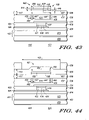
- Structure 412 of FIG. 43 corresponds to manufacturing stage 413 .
- Conductor layer 444 is planarized so that the upper surface of conductor 444 ′ remaining in channel 438 is substantially co-planar with surface 437 of dielectric layer 436 .
- Chemical-mechanical polishing is a non-limiting example of a suitable planarizing technique. It does not matter if the thickness of dielectric layer 436 is reduced somewhat in this process and reference number 437 in FIG. 43 is intended to refer to the surface after planarizing even if not identical to original upper surface 437 of layer 436 . Persons of skill in the art will understand this.
- MFS and/or upper write-line 445 analogous to MFS 34 of FIGS. 1 , 28 - 29 , 31 - 34 .
- Surface 437 and MFS 445 are covered by dielectric layer 446 of thickness 447 and with upper surface 467 .
- Oxides and/or nitrides of silicon, magnesium, magnesium oxides, and/or combinations thereof are non-limiting examples of materials suitable for layer 446 .
- Plasma deposited silicon nitride is preferred for dielectric layer 446 .
- Thickness 447 conveniently determines quiescent spacing or gap 43 between cladding 33 (see FIGS. 28-29 ) and MFS 34 , 445 .
- Cladding layer 448 of thickness 449 is deposited or formed on surface 467 of dielectric layer 446 .
- NiFe, CoFe and other cladding materials already described are non-limiting examples of suitable materials for layer 448 .
- Thickness 449 is usefully in the range of about 0.05 to 0.3 micrometers, more conveniently in the range of about 0.06 to 0.15 micrometers and preferably in the range of about 0.08 to 0.1 micrometers.
- Hard-mask layer 450 of thickness 451 is formed over cladding layer 448 . Tantalum, tantalum oxide, tantalum nitride, tantalum oxy-nitride, magnesium oxide and combinations thereof are non-limiting examples of materials useful for hard mask layer 450 .
- Thickness 451 is usefully in the range of about 0.025 to 0.5 micrometers, more conveniently in the range of about 0.05 to 0.3 micrometers and preferably in the range of about 0.1 to 0.15 micrometers.
- Layers 448 and 450 are then patterned using, for example, a conventional photoresist mask (not shown) and an etching operation to have lateral width 452 and shapes corresponding, for example but not limited to beams 47 , 49 and cladding 33 of FIGS. 31-34 . It is desirable that width 452 of remaining portion 460 of cladding layer 448 at least equal width 457 of channel 438 and therefore of MFS 445 . After such etching, remaining portion 460 of cladding layer 448 corresponds to cladding elements 33 of FIGS. 28-29 , 31 - 34 . Structure 412 results from manufacturing stage 413 .
- Structure 414 of FIG. 44 corresponds to manufacturing stage 415 .
- Masking dielectric layer 454 of thickness 453 is substantially conformally formed or deposited over surface 467 and layers 448 , 450 .
- Thickness 453 is usefully in the range of about 0.05 to 0.4 micrometers, more conveniently in the range of about 0.08 to 0.25 micrometers and preferably in the range of about 0.1 to 0.12 micrometers.
- Silicon oxide is a non-limiting example of a suitable material for layer 454 , but other etch resistant and preferably dielectric materials may also be used.
- Etch mask layer 456 is then desirably deposited or formed over layer 454 and patterned to have opening 461 of width 455 , generally centered above remaining portion 460 of cladding layer 448 . Width 455 should be larger than width 452 of remaining portion 460 of cladding layer 448 (and hard-mask 450 ).
- Structure 414 results from manufacturing stage 415 .
- Structure 416 of FIG. 45 corresponds to manufacturing stage 417 .
- Structure 414 is etched through opening 461 in mask layer 456 to remove those portions of layers 454 and 446 lying within opening 461 and especially those portions of layer 446 underlying remaining portion 460 of layers 448 , 450 .
- Portion 460 of cladding layer 448 (and hard mask 450 ) is now free to move relative to MFS 445 as indicated by deflection arrow 464 .
- Remaining portion 460 of cladding layer corresponds to moveable cladding element 33 described in connection with FIGS. 28-29 , 31 - 34 .
- Spacing 462 between remaining portion 460 and MFS 445 corresponds to gap 43 of FIGS. 28-29 and 31 - 34 .
- FIGS. 37-45 those portions of, for example, layer 450 and/or 448 analogous to regions 47 - 1 , 47 - 2 , 49 - 1 , 49 - 2 of FIGS. 31-34 needed to remotely support remaining portion 460 , are omitted.
- Persons of skill in the art will understand based on the desired configuration and operation of their sensors, how to laterally define beams, diaphragms, or other structures for moveably supporting portion 460 with remaining portion 448 ′ of layer 448 providing cladding element 33 , so as to meet the needs of their particular arrangement.
- FIGS. 46-47 are simplified schematic side views analogous to those of FIGS. 28-29 of sensor 470 employing moveable cladding, according to a still yet further embodiment of the invention.
- Sensor 470 comprises lower write-line 422 , lower interconnect electrode 426 , magnetic tunnel junction 432 and upper interconnect electrode 434 such as have already been described in connection with FIGS. 37-45 and prior figures.
- Sensor 470 further comprises magnetic field source 476 analogous to MFS 34 , 445 but without lateral edge cladding, and with moveable cladding 478 adapted to move in response to sensor input as shown by movement arrow 477 .
- sensor 470 has gap 479 of a first magnitude between cladding 478 and MFS 476 , and in FIG.
- analogous gap 479 ′ is much reduced compared to gap 479 , thereby changing the magnetic field at MTJ 432 , in the same manner as previously described.
- Sensor 470 differs from the implementations illustrated in FIGS. 28-29 and 31 - 45 in that MFS 476 has no lateral edge cladding. Instead, moveable cladding 478 has lateral edges that extend downward so as to slide over the lateral edges of MFS 476 as gap 479 , 479 ′ varies in size. In this manner, an analogous magnetic field focusing affect is provided so that the movement of cladding 478 affects the magnetic field at MTJ provided by MFS 476 . This arrangement is useful but not essential.
- a sensor comprising, a magnetic tunnel junction (MTJ), a magnetic field source (MFS) coupled to the MTJ and adapted to provide a magnetic field thereto, and a magnetic cladding element moveably coupled to the MFS so that when perturbed by an input to the sensor, movement of the cladding element causes the magnetic field at the MTJ provided by the MFS to vary in response to the input to the sensor.
- the MFS is fixedly coupled to the MTJ.
- the MFS comprises auxiliary cladding elements on lateral sides thereof and the magnetic cladding element has a lateral width relative to the MFS to overlap the combination of the MFS and the auxiliary cladding elements.
- the magnetic cladding element has extensions at some lateral edges thereof adapted to engage lateral edges of the MFS as the cladding element approaches the MFS.
- the sensor further comprises a write-line magnetically coupled to the MTJ on an opposite side of the MTJ from the MFS.
- the write-line has further auxiliary magnetic cladding on three sides not facing the MTJ.
- the sensor further comprises a deflectable element supporting the magnetic cladding and coupled to the sensor input.
- a sensor comprising, a magnetic tunnel junction (MTJ) comprising, a first magnetic electrode, a second magnetic electrode, and a dielectric separating the first and second electrodes, adapted to provide tunneling conduction therebetween, wherein the sensor further comprises a magnetic field source (MFS) for providing a magnetic field, fixedly located in proximity to the second magnetic electrode, and magnetic cladding moveably suspended in variable proximity to the MFS so that variation of the proximity of the magnetic cladding to the MFS in response to an input of the sensor causes the magnetic field of the MFS at the MTJ to vary, thereby altering the electrical properties of the MTJ.
- MFS comprises a current carrying conductor.
- the current carrying conductor is U-shaped.
- the MFS comprises a permanent magnet.
- the sensor further comprises a deflectable member for moveably supporting the magnetic cladding in variable proximity to the MFS.
- the magnetic cladding is located between the deflectable member and the MFS.
- the deflectable member comprises tantalum, tantalum oxide, tantalum nitride, silicon, silicon oxide, silicon oxy-nitride, silicon nitride and/or a combination thereof.
- the senor further comprises, a conductive write-line fixedly located spaced apart from a first side of the MTJ, and wherein the MFS is fixedly located spaced apart from a second, opposite, side of the MTJ, and wherein the magnetic cladding is moveably located spaced apart from a side of the MFS not facing the MTJ.
- a method for forming a sensor comprising providing a magnetic tunnel junction (MTJ), providing a magnetic field source (MFS) having a first side coupled to the MTJ, and forming a magnetic cladding, moveably coupled to the MFS on a second, opposite side of the MFS, and adapted to move relative to the MFS in response to input to the sensor, thereby altering the magnetic field provided by the MFS at the MTJ.
- MTJ magnetic tunnel junction
- MFS magnetic field source
- the forming step further comprises, adding a spacer over the MFS, forming the magnetic cladding on the spacer, and removing a portion of the spacer lying between the magnetic cladding and the MFS so that at least a part of the magnetic cladding can move relative to the MFS in response to the sensor input.
- the step of providing the MFS further comprises, providing second magnetic cladding on lateral sides of the MFS, wherein the moveable cladding responsive to the sensor input has sufficient lateral width to at least overlap the lateral width of the MFS plus the second cladding.
- the step of forming the magnetic cladding moveably coupled to the MFS further comprises, bonding a substantially non-magnetic material to the magnetic cladding.
- the substantially non-magnetic material comprises, tantalum, tantalum oxide, tantalum nitride, silicon, silicon oxide, silicon oxy-nitride, silicon nitride and/or a combination thereof.
Landscapes
- Physics & Mathematics (AREA)
- Condensed Matter Physics & Semiconductors (AREA)
- General Physics & Mathematics (AREA)
- Engineering & Computer Science (AREA)
- Computer Hardware Design (AREA)
- Manufacturing & Machinery (AREA)
- Measuring Magnetic Variables (AREA)
- Hall/Mr Elements (AREA)
Abstract
Description
Claims (12)
Priority Applications (1)
| Application Number | Priority Date | Filing Date | Title |
|---|---|---|---|
| US11/584,473 US7602177B2 (en) | 2005-07-29 | 2006-10-19 | Sensor having moveable cladding suspended near a magnetic field source |
Applications Claiming Priority (2)
| Application Number | Priority Date | Filing Date | Title |
|---|---|---|---|
| US11/192,569 US7541804B2 (en) | 2005-07-29 | 2005-07-29 | Magnetic tunnel junction sensor |
| US11/584,473 US7602177B2 (en) | 2005-07-29 | 2006-10-19 | Sensor having moveable cladding suspended near a magnetic field source |
Related Parent Applications (1)
| Application Number | Title | Priority Date | Filing Date |
|---|---|---|---|
| US11/192,569 Continuation-In-Part US7541804B2 (en) | 2005-07-29 | 2005-07-29 | Magnetic tunnel junction sensor |
Publications (2)
| Publication Number | Publication Date |
|---|---|
| US20070159735A1 US20070159735A1 (en) | 2007-07-12 |
| US7602177B2 true US7602177B2 (en) | 2009-10-13 |
Family
ID=37694039
Family Applications (2)
| Application Number | Title | Priority Date | Filing Date |
|---|---|---|---|
| US11/192,569 Expired - Fee Related US7541804B2 (en) | 2005-07-29 | 2005-07-29 | Magnetic tunnel junction sensor |
| US11/584,473 Expired - Fee Related US7602177B2 (en) | 2005-07-29 | 2006-10-19 | Sensor having moveable cladding suspended near a magnetic field source |
Family Applications Before (1)
| Application Number | Title | Priority Date | Filing Date |
|---|---|---|---|
| US11/192,569 Expired - Fee Related US7541804B2 (en) | 2005-07-29 | 2005-07-29 | Magnetic tunnel junction sensor |
Country Status (5)
| Country | Link |
|---|---|
| US (2) | US7541804B2 (en) |
| JP (1) | JP2009503858A (en) |
| KR (1) | KR20080033957A (en) |
| TW (1) | TW200713647A (en) |
| WO (1) | WO2007016011A2 (en) |
Cited By (3)
| Publication number | Priority date | Publication date | Assignee | Title |
|---|---|---|---|---|
| US20090243607A1 (en) * | 2008-03-26 | 2009-10-01 | Mather Phillip G | Magnetic Sensor Design for Suppression of Barkhausen Noise |
| US20110303994A1 (en) * | 2009-02-13 | 2011-12-15 | Colin Robert Jenkins | Mems device and process |
| CN107408986A (en) * | 2015-03-20 | 2017-11-28 | 甲骨文国际公司 | The laser array of security enhancing |
Families Citing this family (20)
| Publication number | Priority date | Publication date | Assignee | Title |
|---|---|---|---|---|
| US7547480B2 (en) * | 2005-10-28 | 2009-06-16 | Everspin Technologies, Inc. | Magnetic tunnel junction pressure sensors and methods |
| US7768083B2 (en) | 2006-01-20 | 2010-08-03 | Allegro Microsystems, Inc. | Arrangements for an integrated sensor |
| US7483295B2 (en) * | 2007-04-23 | 2009-01-27 | Mag Ic Technologies, Inc. | MTJ sensor including domain stable free layer |
| US7965077B2 (en) | 2008-05-08 | 2011-06-21 | Everspin Technologies, Inc. | Two-axis magnetic field sensor with multiple pinning directions |
| US8482968B2 (en) * | 2010-11-13 | 2013-07-09 | International Business Machines Corporation | Non-volatile magnetic tunnel junction transistor |
| US9395410B2 (en) * | 2011-06-06 | 2016-07-19 | Iii Holdings 1, Llc | Integrated circuit with sensing unit and method for using the same |
| US8767446B2 (en) | 2011-10-12 | 2014-07-01 | International Business Machines Corporation | Multi-bit spin-momentum-transfer magnetoresistence random access memory with single magnetic-tunnel-junction stack |
| US8975891B2 (en) | 2011-11-04 | 2015-03-10 | Honeywell International Inc. | Apparatus and method for determining in-plane magnetic field components of a magnetic field using a single magnetoresistive sensor |
| DE112013006523T5 (en) | 2013-03-15 | 2015-10-22 | Intel Corporation | Embedded magnetic tunnel contacts comprehensive logic chip |
| DE102013211626A1 (en) | 2013-06-20 | 2014-12-24 | Robert Bosch Gmbh | Sensor and method for detecting a position of an effective surface of the sensor |
| JP6105817B2 (en) * | 2013-11-01 | 2017-03-29 | 中国科学院物理研究所 | Nanomagnetic multilayer film for temperature sensor and its manufacturing method |
| US9543067B2 (en) | 2013-12-20 | 2017-01-10 | Nxp Usa, Inc. | Magnetic pre-conditioning of magnetic sensors |
| DE102014109701A1 (en) * | 2014-07-10 | 2016-01-14 | Epcos Ag | sensor |
| EP2966453B1 (en) * | 2014-07-11 | 2018-10-31 | Crocus Technology | MLU based accelerometer using a magnetic tunnel junction |
| US10082431B2 (en) | 2015-07-17 | 2018-09-25 | Honeywell International Inc. | System and methods for magnetic tunnel junction pressure sensors |
| US10996125B2 (en) * | 2017-05-17 | 2021-05-04 | Infineon Technologies Ag | Pressure sensors and method for forming a MEMS pressure sensor |
| US10935612B2 (en) | 2018-08-20 | 2021-03-02 | Allegro Microsystems, Llc | Current sensor having multiple sensitivity ranges |
| CN111863865B (en) * | 2019-04-24 | 2024-04-12 | 上海磁宇信息科技有限公司 | Pseudo-magnetic tunnel junction unit |
| US10830841B1 (en) | 2019-06-19 | 2020-11-10 | International Business Machines Corporation | Magnetic tunnel junction performance monitoring based on magnetic field coupling |
| US11567108B2 (en) | 2021-03-31 | 2023-01-31 | Allegro Microsystems, Llc | Multi-gain channels for multi-range sensor |
Citations (8)
| Publication number | Priority date | Publication date | Assignee | Title |
|---|---|---|---|---|
| US4916393A (en) * | 1987-12-16 | 1990-04-10 | Commissariat A L'energie Atomique | Continuous vectorial magnetometer with capacitive magnetostriction pickup and gradiometer involving the application of this pickup |
| US5900729A (en) * | 1997-03-20 | 1999-05-04 | International Business Machines Corporation | Magnetic force microscopy probe with integrated coil |
| US5925818A (en) * | 1994-08-15 | 1999-07-20 | The Regents Of The University Of Calif. | Method and apparatus for magnetic force control of a scanning probe |
| US6657431B2 (en) * | 2000-06-06 | 2003-12-02 | Brown University Research Foundation | Scanning magnetic microscope having improved magnetic sensor |
| US20040023365A1 (en) | 2002-07-31 | 2004-02-05 | Bradley N. Engel | High sensitivity sensor for tagged magnetic bead bioassays |
| US6714442B1 (en) | 2003-01-17 | 2004-03-30 | Motorola, Inc. | MRAM architecture with a grounded write bit line and electrically isolated read bit line |
| US6740947B1 (en) * | 2002-11-13 | 2004-05-25 | Hewlett-Packard Development Company, L.P. | MRAM with asymmetric cladded conductor |
| US6897650B2 (en) * | 2002-02-11 | 2005-05-24 | International Business Machines Corporation | Magnetic-field sensor device |
Family Cites Families (11)
| Publication number | Priority date | Publication date | Assignee | Title |
|---|---|---|---|---|
| US5166612A (en) * | 1990-11-13 | 1992-11-24 | Tektronix, Inc. | Micromechanical sensor employing a squid to detect movement |
| JPH0961454A (en) * | 1995-08-29 | 1997-03-07 | Tokin Corp | Semiconductor magnetic operation type acceleration sensor |
| US6185079B1 (en) * | 1998-11-09 | 2001-02-06 | International Business Machines Corporation | Disk drive with thermal asperity reduction circuitry using a magnetic tunnel junction sensor |
| US6414086B1 (en) * | 2000-02-29 | 2002-07-02 | Howmedica Osteonics Corp. | Compositions, processes and methods of improving the wear resistance of prosthetic medical devices |
| JP2002026419A (en) * | 2000-07-07 | 2002-01-25 | Sanken Electric Co Ltd | Magnetoelectric converter |
| US6555858B1 (en) * | 2000-11-15 | 2003-04-29 | Motorola, Inc. | Self-aligned magnetic clad write line and its method of formation |
| JP3498737B2 (en) * | 2001-01-24 | 2004-02-16 | ヤマハ株式会社 | Manufacturing method of magnetic sensor |
| US6906511B2 (en) * | 2001-05-08 | 2005-06-14 | Analog Devices, Inc. | Magnetic position detection for micro machined optical element |
| JP3835354B2 (en) * | 2001-10-29 | 2006-10-18 | ヤマハ株式会社 | Magnetic sensor |
| US7183765B2 (en) * | 2003-06-26 | 2007-02-27 | The Regents Of The University Of California | Micro-position sensor using faraday effect |
| ATE386949T1 (en) | 2003-12-23 | 2008-03-15 | Nxp Bv | HIGHLY SENSITIVE MAGNETIC BUILT-IN CURRENT SENSOR |
-
2005
- 2005-07-29 US US11/192,569 patent/US7541804B2/en not_active Expired - Fee Related
-
2006
- 2006-07-24 KR KR1020087002294A patent/KR20080033957A/en not_active Withdrawn
- 2006-07-24 JP JP2008524013A patent/JP2009503858A/en active Pending
- 2006-07-24 WO PCT/US2006/028576 patent/WO2007016011A2/en not_active Ceased
- 2006-07-28 TW TW095127621A patent/TW200713647A/en unknown
- 2006-10-19 US US11/584,473 patent/US7602177B2/en not_active Expired - Fee Related
Patent Citations (8)
| Publication number | Priority date | Publication date | Assignee | Title |
|---|---|---|---|---|
| US4916393A (en) * | 1987-12-16 | 1990-04-10 | Commissariat A L'energie Atomique | Continuous vectorial magnetometer with capacitive magnetostriction pickup and gradiometer involving the application of this pickup |
| US5925818A (en) * | 1994-08-15 | 1999-07-20 | The Regents Of The University Of Calif. | Method and apparatus for magnetic force control of a scanning probe |
| US5900729A (en) * | 1997-03-20 | 1999-05-04 | International Business Machines Corporation | Magnetic force microscopy probe with integrated coil |
| US6657431B2 (en) * | 2000-06-06 | 2003-12-02 | Brown University Research Foundation | Scanning magnetic microscope having improved magnetic sensor |
| US6897650B2 (en) * | 2002-02-11 | 2005-05-24 | International Business Machines Corporation | Magnetic-field sensor device |
| US20040023365A1 (en) | 2002-07-31 | 2004-02-05 | Bradley N. Engel | High sensitivity sensor for tagged magnetic bead bioassays |
| US6740947B1 (en) * | 2002-11-13 | 2004-05-25 | Hewlett-Packard Development Company, L.P. | MRAM with asymmetric cladded conductor |
| US6714442B1 (en) | 2003-01-17 | 2004-03-30 | Motorola, Inc. | MRAM architecture with a grounded write bit line and electrically isolated read bit line |
Non-Patent Citations (2)
| Title |
|---|
| Li et al. "MEMS Microbridge Vibration Monitoring Using Spin-Valve Sensors," IEEE Transactions on Magnetics, vol. 38, issue 5, pp. 3371-3373, 2002. |
| Papautsky et al., "A Low-Temperature IC-Compatible Process for Fabricating Surface-Micromachined Metallic Microchannels,". J. of MEMS, vol. 7, No. 2, pp. 267-273, 1998. |
Cited By (5)
| Publication number | Priority date | Publication date | Assignee | Title |
|---|---|---|---|---|
| US20090243607A1 (en) * | 2008-03-26 | 2009-10-01 | Mather Phillip G | Magnetic Sensor Design for Suppression of Barkhausen Noise |
| US8242776B2 (en) * | 2008-03-26 | 2012-08-14 | Everspin Technologies, Inc. | Magnetic sensor design for suppression of barkhausen noise |
| US20110303994A1 (en) * | 2009-02-13 | 2011-12-15 | Colin Robert Jenkins | Mems device and process |
| CN107408986A (en) * | 2015-03-20 | 2017-11-28 | 甲骨文国际公司 | The laser array of security enhancing |
| CN107408986B (en) * | 2015-03-20 | 2020-01-21 | 甲骨文国际公司 | Safety-enhanced laser array |
Also Published As
| Publication number | Publication date |
|---|---|
| TW200713647A (en) | 2007-04-01 |
| US7541804B2 (en) | 2009-06-02 |
| JP2009503858A (en) | 2009-01-29 |
| WO2007016011A3 (en) | 2008-09-12 |
| WO2007016011A2 (en) | 2007-02-08 |
| US20070159735A1 (en) | 2007-07-12 |
| KR20080033957A (en) | 2008-04-17 |
| US20070025027A1 (en) | 2007-02-01 |
Similar Documents
| Publication | Publication Date | Title |
|---|---|---|
| US7602177B2 (en) | Sensor having moveable cladding suspended near a magnetic field source | |
| US7414396B2 (en) | Sensor with magnetic tunnel junction and moveable magnetic field source | |
| US7355822B2 (en) | Superparamagnetic field sensing device | |
| JP5297075B2 (en) | Magnetic sensor, manufacturing method thereof, current detection method, and current detection apparatus | |
| EP3199964B1 (en) | Magnetic field sensor with permanent magnet biasing technical field of the invention | |
| CN102859382A (en) | Integrated magnetometer and method of manufacturing the same | |
| US11428758B2 (en) | High sensitivity TMR magnetic sensor | |
| US7220602B2 (en) | Magnetic tunnel junction sensor method | |
| US7444738B2 (en) | Method for tunnel junction sensor with magnetic cladding | |
| JP2022510249A (en) | Manufacturing method of magnetic sensor, Hall sensor and Hall sensor using the abnormal Hall effect | |
| EP1722207B1 (en) | Magnetic temperature sensor device, manufacturing process and detection process therefrom | |
| JP3705702B2 (en) | Magnetic device | |
| JP2008251796A (en) | Magnetic recording device | |
| US9368550B2 (en) | Application specific integrated circuit with integrated magnetic sensor | |
| US10096767B2 (en) | Elongated magnetoresistive tunnel junction structure | |
| KR100441779B1 (en) | Magnetoesistance-type vibration sensor and a method for sensing vibration using the same | |
| US7268543B2 (en) | Device for detecting magnetic fields and related detecting methods | |
| EP3022569A1 (en) | Application specific integrated circuit with integrated magnetic sensor |
Legal Events
| Date | Code | Title | Description |
|---|---|---|---|
| AS | Assignment |
Owner name: FREESCALE SEMICONDUCTOR, INC., TEXAS Free format text: ASSIGNMENT OF ASSIGNORS INTEREST;ASSIGNORS:BUTCHER, BRIAN R.;ENGEL, BRADLEY N.;SMITH, KENNETH H.;REEL/FRAME:018452/0351 Effective date: 20061016 |
|
| AS | Assignment |
Owner name: EVERSPIN TECHNOLOGIES, INC., ARIZONA Free format text: ASSIGNMENT OF ASSIGNORS INTEREST;ASSIGNOR:FREESCALE SEMICONDUCTOR, INC.;REEL/FRAME:022366/0467 Effective date: 20090225 Owner name: EVERSPIN TECHNOLOGIES, INC.,ARIZONA Free format text: ASSIGNMENT OF ASSIGNORS INTEREST;ASSIGNOR:FREESCALE SEMICONDUCTOR, INC.;REEL/FRAME:022366/0467 Effective date: 20090225 |
|
| AS | Assignment |
Owner name: EVERSPIN TECHNOLOGIES, INC., ARIZONA Free format text: RELEASE BY SECURED PARTY;ASSIGNOR:CITIBANK, N.A.;REEL/FRAME:024767/0398 Effective date: 20080605 |
|
| FPAY | Fee payment |
Year of fee payment: 4 |
|
| AS | Assignment |
Owner name: EVERSPIN TECHNOLOGIES, INC., ARIZONA Free format text: ASSIGNMENT OF ASSIGNORS INTEREST;ASSIGNOR:FREESCALE SEMICONDUCTOR, INC.;REEL/FRAME:036084/0057 Effective date: 20080606 |
|
| REMI | Maintenance fee reminder mailed | ||
| LAPS | Lapse for failure to pay maintenance fees |
Free format text: PATENT EXPIRED FOR FAILURE TO PAY MAINTENANCE FEES (ORIGINAL EVENT CODE: EXP.) |
|
| STCH | Information on status: patent discontinuation |
Free format text: PATENT EXPIRED DUE TO NONPAYMENT OF MAINTENANCE FEES UNDER 37 CFR 1.362 |
|
| FP | Lapsed due to failure to pay maintenance fee |
Effective date: 20171013 |