US7598542B2 - SRAM devices and methods of fabricating the same - Google Patents
SRAM devices and methods of fabricating the same Download PDFInfo
- Publication number
- US7598542B2 US7598542B2 US11/027,077 US2707704A US7598542B2 US 7598542 B2 US7598542 B2 US 7598542B2 US 2707704 A US2707704 A US 2707704A US 7598542 B2 US7598542 B2 US 7598542B2
- Authority
- US
- United States
- Prior art keywords
- layer
- gate electrode
- common gate
- forming
- drive transistor
- Prior art date
- Legal status (The legal status is an assumption and is not a legal conclusion. Google has not performed a legal analysis and makes no representation as to the accuracy of the status listed.)
- Expired - Fee Related, expires
Links
- 238000000034 method Methods 0.000 title claims abstract description 22
- 239000010410 layer Substances 0.000 claims description 112
- 238000002955 isolation Methods 0.000 claims description 24
- 229910021332 silicide Inorganic materials 0.000 claims description 23
- 239000000758 substrate Substances 0.000 claims description 21
- 239000011229 interlayer Substances 0.000 claims description 20
- FVBUAEGBCNSCDD-UHFFFAOYSA-N silicide(4-) Chemical compound [Si-4] FVBUAEGBCNSCDD-UHFFFAOYSA-N 0.000 claims description 20
- 239000004065 semiconductor Substances 0.000 claims description 12
- 239000002184 metal Substances 0.000 claims description 11
- 229910052751 metal Inorganic materials 0.000 claims description 11
- 238000004519 manufacturing process Methods 0.000 claims description 7
- 230000003647 oxidation Effects 0.000 claims description 7
- 238000007254 oxidation reaction Methods 0.000 claims description 7
- 229910052710 silicon Inorganic materials 0.000 claims description 7
- 239000010703 silicon Substances 0.000 claims description 7
- 239000004020 conductor Substances 0.000 claims description 6
- 229910052802 copper Inorganic materials 0.000 claims description 6
- 238000000137 annealing Methods 0.000 claims description 4
- 229910052759 nickel Inorganic materials 0.000 claims description 4
- 229910021420 polycrystalline silicon Inorganic materials 0.000 claims description 4
- 229920005591 polysilicon Polymers 0.000 claims description 4
- 229910052719 titanium Inorganic materials 0.000 claims description 4
- 239000005368 silicate glass Substances 0.000 claims description 3
- 125000006850 spacer group Chemical group 0.000 claims description 3
- XUIMIQQOPSSXEZ-UHFFFAOYSA-N Silicon Chemical compound [Si] XUIMIQQOPSSXEZ-UHFFFAOYSA-N 0.000 claims 3
- 239000000463 material Substances 0.000 claims 3
- 229910052750 molybdenum Inorganic materials 0.000 claims 3
- 229910045601 alloy Inorganic materials 0.000 claims 2
- 239000000956 alloy Substances 0.000 claims 2
- 238000000151 deposition Methods 0.000 claims 1
- 238000002844 melting Methods 0.000 claims 1
- 238000000059 patterning Methods 0.000 claims 1
- 230000010354 integration Effects 0.000 abstract description 6
- 238000010586 diagram Methods 0.000 description 6
- 238000005520 cutting process Methods 0.000 description 5
- 238000005468 ion implantation Methods 0.000 description 2
- 238000005549 size reduction Methods 0.000 description 2
- 238000005530 etching Methods 0.000 description 1
- 239000011261 inert gas Substances 0.000 description 1
- 230000003068 static effect Effects 0.000 description 1
Images


Classifications
-
- H—ELECTRICITY
- H10—SEMICONDUCTOR DEVICES; ELECTRIC SOLID-STATE DEVICES NOT OTHERWISE PROVIDED FOR
- H10B—ELECTRONIC MEMORY DEVICES
- H10B10/00—Static random access memory [SRAM] devices
-
- H—ELECTRICITY
- H10—SEMICONDUCTOR DEVICES; ELECTRIC SOLID-STATE DEVICES NOT OTHERWISE PROVIDED FOR
- H10B—ELECTRONIC MEMORY DEVICES
- H10B10/00—Static random access memory [SRAM] devices
- H10B10/12—Static random access memory [SRAM] devices comprising a MOSFET load element
-
- Y—GENERAL TAGGING OF NEW TECHNOLOGICAL DEVELOPMENTS; GENERAL TAGGING OF CROSS-SECTIONAL TECHNOLOGIES SPANNING OVER SEVERAL SECTIONS OF THE IPC; TECHNICAL SUBJECTS COVERED BY FORMER USPC CROSS-REFERENCE ART COLLECTIONS [XRACs] AND DIGESTS
- Y10—TECHNICAL SUBJECTS COVERED BY FORMER USPC
- Y10S—TECHNICAL SUBJECTS COVERED BY FORMER USPC CROSS-REFERENCE ART COLLECTIONS [XRACs] AND DIGESTS
- Y10S257/00—Active solid-state devices, e.g. transistors, solid-state diodes
- Y10S257/903—FET configuration adapted for use as static memory cell
Definitions
- the present disclosure relates to SRAM devices and methods of fabricating the same, by which a process margin and degree of device integration are enhanced by reducing the number of contact holes of an SRAM device unit cell using local interconnection.
- a unit cell of a static random access memory includes six transistors (6-Tr). More specifically, a unit cell typically includes two drive transistors, two access transistors, and two load elements.
- FIG. 1 is a circuit diagram of the prior art SRAM device unit cell.
- FIG. 2 is a layout of the prior art SRAM device unit cell.
- the SRAM device unit cell includes access transistors Q 1 ( 250 ) and Q 3 ( 260 ) having gates connected to a wordline WL and drains connected to positive and negative bitlines BL and/BL, respectively.
- the SRAM device unit cell also includes load elements Q 5 ( 210 ) and Q 6 ( 220 ) having their sources connected to a power voltage Vcc.
- the unit cell also includes a positive cell node N which is commonly connected to a drain of the load element Q 5 ( 210 ) and to the source of the access transistors Q 1 ( 250 ).
- the unit cell also has a negative cell node/N which is commonly connected to a drain of the load element Q 6 ( 220 ) and to the source of the access transistors Q 3 ( 260 ).
- the unit cell is further provided with drive transistors Q 2 ( 230 ) and Q 4 ( 240 ).
- the drive transistor Q 2 is connected to the drain of the load element Q 5 .
- the drive transistor Q 4 is connected to the drain of the load element Q 6 .
- the gates of the drive transistors Q 2 , Q 4 are respectively connected to the gates of the load elements Q 5 , Q 6 in a CMOS configuration. Further, the gates of the drive transistors Q 2 ( 230 ), Q 4 ( 240 ) are cross-linked to the positive and negative cell nodes N,/N, respectively.
- the area enclosed by a dotted-line square in FIG. 2 corresponds to the unit cell of the 6-Tr SRAM device. Each area enclosed by a solid line within the unit cell corresponds to an active area. Moreover, each hatched square indicates a contact hole 206 .
- a common gate electrode 271 is provided to apply a sync signal to the gates of the load element 210 and the drive transistor 230 .
- Upper metal lines (not shown in the drawing) are formed on an insulating inter layer covering the six transistors.
- Contact holes are formed in the insulating interlayer to connect the six transistors to the upper metal lines.
- Each of the contact holes 206 is filled with a conductive plug.
- eight and half (8.5) contact holes are formed for the connections between the transistors and the metal lines.
- the 8.5 contact holes include 6.5 contact holes for connections to the junctions (source/drain) of the transistors and 2 contact holes for connection to the common gate electrodes of the transistors.
- the unit cell area or size of the SRAM device is reduced as well.
- the unit cell of the 6-Tr SRAM device requires the 8.5 contact holes which occupy a considerable fixed area within the unit cell.
- the number of contact holes required for the unit cell of the SRAM device must be lowered as the design rule is reduced.
- FIG. 3 is a cross-sectional view of the SRAM device unit cell in FIG. 2 taken along cutting line A-A′.
- a field oxide layer 202 is provided in a field area to define an active area of a semiconductor substrate 201 .
- Gate electrodes 203 , 204 of a drive transistor and a load element are formed in the active areas of the substrate 201 .
- Sources S and drains D are provided to on opposite sides of the gate electrodes 203 , 204 .
- a gate insulating layer (not shown in the drawing) is provided beneath each of the gate electrodes 203 , 204 .
- a spacer (not shown in the drawing) may be provided on each sidewall of the gate electrodes 203 , 204 .
- a common gate electrode 271 is formed between the gate electrodes 203 , 204 to apply a sync signal to the gate electrodes 203 , 204 of the load element and the drive transistor.
- An insulating layer 205 is formed on the substrate 201 including the common gate electrode 271 .
- An upper line (not shown in the drawing) is formed on the insulating interlayer 205 .
- the source/drain S/D and the common gate electrode 271 are electrically connected to the upper line via respective plugs 207 .
- the plugs 207 fill contact holes 206 provided in the insulating interlayer 205 .
- the contact holes 206 are formed by selectively etching the insulating interlayer 205 to expose two junction layers (source or drain) of the two transistors and the common gate electrode 271 .
- the contact holes provided for the load element, the common gate electrode 271 , and the drive transistor are aligned on almost the same line. Since the contact holes are nearly aligned on the same straight line and are densely aggregated, the process margin is lowered due to the reduced design rule.
- FIG. 1 is a circuit diagram of a prior art SRAM device unit cell.
- FIG. 2 is a diagram illustrating the layout of the prior art SRAM device unit cell of FIG. 1 .
- FIG. 3 is a cross-sectional illustration of the SRAM device unit cell of FIG. 2 taken along cutting line A-A′ of FIG. 2 .
- FIG. 4 is a diagram illustrating the layout of an example SRAM device unit cell constructed in accordance with the teachings of the present invention.
- FIG. 5 is a cross-sectional view of the example SRAM device unit cell taken along cutting line B-B′ of FIG. 4 .
- FIGS. 6A to 6D are cross-sectional views illustrating an example method of fabricating an SRAM device performed in accordance with the teachings of the present invention.
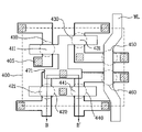
- FIG. 4 is a diagram illustrating the layout of an example SRAM device unit cell constructed in accordance with the teachings of the present invention.
- an example unit cell of the SRAM device includes six transistors. In particular, it includes a pair of load elements 410 , 420 , a pair of drive transistors 430 , 440 , and a pair of access transistors 450 , 460 aligned in a row.
- the load elements 410 , 420 and the drive transistors 430 , 440 are densely aggregated.
- the access transistors 450 , 460 are provided to one side of the drive transistors 430 , 440 .
- the gates of the access transistors 450 , 460 are connected to a wordline WL.
- the gate electrodes 411 , 431 of the first lead element and the first drive transistor are connected in one body.
- a common gate electrode 471 is provided at one end to transfer a sync signal to the first load element 410 and the first drive transistor 430 upon receiving an electric signal from an upper line (not shown in the drawing).
- another common gate electrode (not shown in the drawing) for the second load element 420 and the second drive transistor 440 are provided to another unit cell.
- the common gate electrode pattern 471 of the first load element and the first drive transistor is overlapped with active areas, (i.e., source/drain regions), of the second load element 420 and the second drive transistor 440 .
- the common gate electrode pattern 471 can be formed of doped polysilicon.
- a plurality of contact holes 405 for enabling electrical connections to upper lines are formed on the active areas and the gates such as the common gate electrodes and the like.
- the unit cell of the illustrated example SRAM device includes six and half (6.5) contact holes 405 . Specifically, there are two contact holes on the gate pattern of the transistors including the common gate electrode 471 , and four and one-half contact holes on the junction layers (source/drain regions) of the transistors. Thus, the total number (6.5) of contact holes in the illustrated example SRAM device is smaller than the total number (8.5) of contact holes in the prior art device described above.
- two contact holes are located on the gate pattern including the common gate electrode in both the example SRAM device of FIG. 4 and the prior art device described above.
- the example SRAM devices of FIG. 4 has four and one-half contact holes on the junction layers of the transistors, whereas the prior art SRAM device described above has six and one-half contact holes.
- the contact holes are provided for electrical connections to the upper line of the junction layers of the first load element 210 , the common gate electrode 271 , and the first drive transistor 230 aligned on the same line.
- one end of the common gate electrode pattern is overlapped with the junction layers of the second load element 420 and the second drive transistor 440 . Consequently, one contact hole is formed for the electrical connection to the upper line on one prescribed portion of the common gate electrode pattern.
- the common gate electrode pattern of FIG. 4 overlaps with the second load element and the second drive transistor, only one contact (and, thus, one contact hole) is needed.
- FIG. 5 is a cross-sectional diagram of the example SRAM device unit cell of FIG. 4 taken along cutting line B-B′ of FIG. 4 .
- a device isolation layer 402 is provided in a field area by STI (shallow trench isolation) or LOCOS (local oxidation of silicon) to define active areas in a semiconductor substrate 401 .
- Gate electrodes 421 , 441 of the second load element and the second drive transistor are respectively formed on the active areas isolated by the device isolation layer 402 .
- Junction layers, (i.e., source/drain regions S/D), are formed in the substrate on opposite sides of the gate electrodes 421 , 441 .
- a common gate electrode pattern 471 is formed on the substrate 401 above the device isolation layer 402 and portions of the junction layers of the second load element and the second drive transistor.
- the common gate electrode pattern 471 can be formed of doped polysilicon.
- a salicide (self-aligned silicide) layer 403 is formed on the common gate electrode pattern 411 and the junction layers D of the second load element and the second drive transistor.
- the salicide layer 403 is formed of Ti-silicide, Co-silicide, Mo-silicide, or the like.
- An insulating interlayer 404 is formed on the substrate 401 including on the salicide layer 403 .
- a contact hole 405 is formed in the insulating interlayer 404 to expose the salicide layer 403 .
- a metal layer fills the contact hole 405 to form a conductive plug 406 .
- An upper line formed, for example, of Al, Cu, or the like, is formed on the insulating interlayer 404 and on the plug 406 .
- the contact hole 405 may be formed on any portion of the salicide layer 403 as long as the salicide layer 403 is exposed.
- FIGS. 6A to 6D are cross-sectional views taken along cutting line B-B′ in FIG. 4 and illustrate the method of fabricating the SRAM device at various points in time.
- a device isolation layer 402 is formed in a field area of the semiconductor substrate 401 by STI (shallow trench isolation) or LOCOS (local oxidation of silicon) to define active areas in the semiconductor substrate 401 .
- STI shallow trench isolation
- LOCOS local oxidation of silicon
- An oxide layer (not shown in the drawing) is grown on the active areas of the semiconductor substrate 401 by thermal oxidation to form a gate oxide layer (not shown in the drawing).
- a conductor layer for forming gate electrodes is deposited on the oxide layer.
- the conductor layer is formed of heavily doped polysilicon.
- the conductor layer and the oxide layer are selectively patterned to form a gate electrode 421 of a second load element, a common gate electrode 471 , and a gate electrode 441 of a second drive transistor.
- junction layers i.e., sources S and drains D
- Spacers may be formed on the sidewalls of the gate electrodes 421 , 441 prior to forming the sources S and drains D. Further, LDD (lightly doped drain) regions can be formed in the active areas on opposite sides of the gate electrodes 421 , 441 by light ion implantation.
- junction layers i.e., sources and drains
- a low specific-resistance, high-melting-point metal layer is formed on the illustrated substrate 401 and on the gate electrode pattern 471 using Ti, Co, Ni, or the like.
- annealing is performed on the substrate in an ambience of inert gas such as N 2 , He, or Ar by RTP (rapid thermal processing) or using a furnace.
- inert gas such as N 2 , He, or Ar
- RTP rapid thermal processing
- the high-melting-point metal layer on the gate electrodes and junction layers reacts with the silicon of the semiconductor substrate and the gate electrodes to turn into a silicide layer.
- the portions of the high-melting-point metal layer which fail to react with silicon are removed. After those portions of the high-melting-point metal layer have been removed, a salicide layer 403 is formed.
- the salicide layer 403 can be selectively formed on only the common gate electrode pattern 471 and the junction layers.
- an insulating interlayer 404 is formed on the substrate 401 and on the salicide layer 403 .
- the insulating interlayer 404 is formed of oxide such as BPSG (borophosphorous silicate glass) or the like.
- a prescribed portion of the insulating interlayer 404 is then etched to form a contact hole 405 .
- the contact hole 405 is formed to expose a portion of the salicide layer 403 .
- Dotted lines in the drawing indicate alternate contact holes 405 that can be formed on the salicide layer 403 .
- the contact hole 405 is filled with a conductor metal layer to form a conductive plug 406 .
- an upper line (not shown in the drawing) is formed on the insulating interlayer 404 in contact with the plug 406 .
- the plug 406 and the upper line can be formed by a damascene process.
- the common gate electrode pattern 471 is formed on the area including: (a) the junction layer of the second load element and (b) the junction layer of the second drive transistor, and the salicide layer 403 is formed on the common gate electrode 471 and the corresponding junction layers.
- the contact hole 405 exposing a portion of the salicide layer 403 can function as the contact holes for the junction layer of the second load element, for the junction layer of the second drive transistor, and for the common gate electrode of the prior art. Therefore, the example device of FIG. 6D employs only one contact hole instead of the three contact holes in the prior art. As a result, the above disclosed method can achieve a simplified process and a device size reduction by providing one contact hole for electrical connections with an upper line of a load element, a drive transistor, and a common gate electrode.
- a disclosed example SRAM device includes first and second load elements; first and second drive transistors; a common gate electrode connected in one body to a gate electrode of the first load element and a gate electrode of the first drive transistor to apply a sync signal to the gate electrodes, the common gate electrode being overlapped with a junction layer of the second load element and a junction layer region of the second drive transistor, the common gate electrode being electrically connected to an upper line via one contact hole filled with a plug.
- the SRAM device further includes a silicide layer on the junction layer of the second load element, the junction layer region of the second drive transistor, and the common gate electrode.
- the contact hole is formed to expose a portion of the silicide layer.
- a disclosed example method of fabricating an SRAM device having first and second load elements and first and second drive transistors comprises: forming a device isolation layer on a semiconductor substrate to define active areas therein; forming gate electrodes of the second load element and the second drive transistor on the active areas isolated by the device isolation layer; forming a common gate electrode of the first load element and the first drive transistor on prescribed portions of the active areas and the device isolation layer; forming source/drain regions on opposite sides of each of the gate electrodes of the second load element and the second drive transistor; forming an insulating interlayer on the substrate including the gate electrodes and the common gate electrode; forming a contact hole in the insulating interlayer to expose a portion of the common gate electrode, and forming a plug filing the contact hole.
- the method further includes forming a silicide layer on the source/drain regions and the common gate electrode prior to forming the insulating layer.
- the contact hole is formed to expose a portion of the silicide layer.
- a disclosed example SRAM device includes a semiconductor substrate having active areas defined by a device isolation layer; gate electrodes of a second load element and a second drive transistor on the active areas isolated by the device isolation layer; a common gate electrode of a first load element and a first drive transistor on portions of the active areas and the device isolation layer; source/drain regions on opposite sides of the gate electrodes of the second load element and the second drive transistor; an insulating interlayer on the gate electrodes and the common gate electrode; a contact hole in the insulating interlayer to expose a portion of the common gate electrode, and a plug in the contact hole.
- the SRAM device further includes a silicide layer on the source/drain regions and the common gate electrode.
- the contact hole is formed to expose a portion of the silicide layer.
Landscapes
- Semiconductor Memories (AREA)
Abstract
Description
Claims (20)
Applications Claiming Priority (2)
| Application Number | Priority Date | Filing Date | Title |
|---|---|---|---|
| KR2003-0101390 | 2003-12-31 | ||
| KR1020030101390A KR100573276B1 (en) | 2003-12-31 | 2003-12-31 | SRAM device and its manufacturing method |
Publications (2)
| Publication Number | Publication Date |
|---|---|
| US20050141268A1 US20050141268A1 (en) | 2005-06-30 |
| US7598542B2 true US7598542B2 (en) | 2009-10-06 |
Family
ID=34698876
Family Applications (1)
| Application Number | Title | Priority Date | Filing Date |
|---|---|---|---|
| US11/027,077 Expired - Fee Related US7598542B2 (en) | 2003-12-31 | 2004-12-29 | SRAM devices and methods of fabricating the same |
Country Status (2)
| Country | Link |
|---|---|
| US (1) | US7598542B2 (en) |
| KR (1) | KR100573276B1 (en) |
Cited By (3)
| Publication number | Priority date | Publication date | Assignee | Title |
|---|---|---|---|---|
| US20150035083A1 (en) * | 2013-08-05 | 2015-02-05 | Semiconductor Manufacturing International (Shanghai) Corporation | Mos transistors and fabrication method thereof |
| US20160293590A1 (en) * | 2013-08-16 | 2016-10-06 | Taiwan Semiconductor Manufacturing Company, Ltd. | Mask Optimization For Multi-Layer Contacts |
| US9997403B2 (en) * | 2016-02-18 | 2018-06-12 | International Business Machines Corporation | Metal layer tip to tip short |
Families Citing this family (3)
| Publication number | Priority date | Publication date | Assignee | Title |
|---|---|---|---|---|
| KR100556747B1 (en) * | 2003-11-26 | 2006-03-10 | 엘지전자 주식회사 | Field emission devices |
| JP4899085B2 (en) | 2006-03-03 | 2012-03-21 | 富士通セミコンダクター株式会社 | Semiconductor device and manufacturing method thereof |
| US7791109B2 (en) * | 2007-03-29 | 2010-09-07 | International Business Machines Corporation | Metal silicide alloy local interconnect |
Citations (6)
| Publication number | Priority date | Publication date | Assignee | Title |
|---|---|---|---|---|
| US4939567A (en) * | 1987-12-21 | 1990-07-03 | Ibm Corporation | Trench interconnect for CMOS diffusion regions |
| US6015996A (en) * | 1996-08-05 | 2000-01-18 | Samsung Electronics Co., Ltd. | Cell structure of an improved CMOS static RAM and its fabrication method |
| US6090673A (en) * | 1998-10-20 | 2000-07-18 | International Business Machines Corporation | Device contact structure and method for fabricating same |
| US6255701B1 (en) * | 1995-11-06 | 2001-07-03 | Seiko Epson Corporation | Semiconductor device containing local interconnection and method of manufacturing the same |
| US6313510B1 (en) * | 1997-08-22 | 2001-11-06 | Samsung Electronics Co., Ltd. | Integrated circuits including metal silicide contacts extending between a gate electrode and a source/drain region |
| US7087493B1 (en) * | 2000-08-09 | 2006-08-08 | Texas Instruments Incorporated | Memory with 6T small aspect ratio cells having metal—1 elements physically connected to metal—0 elements |
-
2003
- 2003-12-31 KR KR1020030101390A patent/KR100573276B1/en not_active Expired - Fee Related
-
2004
- 2004-12-29 US US11/027,077 patent/US7598542B2/en not_active Expired - Fee Related
Patent Citations (6)
| Publication number | Priority date | Publication date | Assignee | Title |
|---|---|---|---|---|
| US4939567A (en) * | 1987-12-21 | 1990-07-03 | Ibm Corporation | Trench interconnect for CMOS diffusion regions |
| US6255701B1 (en) * | 1995-11-06 | 2001-07-03 | Seiko Epson Corporation | Semiconductor device containing local interconnection and method of manufacturing the same |
| US6015996A (en) * | 1996-08-05 | 2000-01-18 | Samsung Electronics Co., Ltd. | Cell structure of an improved CMOS static RAM and its fabrication method |
| US6313510B1 (en) * | 1997-08-22 | 2001-11-06 | Samsung Electronics Co., Ltd. | Integrated circuits including metal silicide contacts extending between a gate electrode and a source/drain region |
| US6090673A (en) * | 1998-10-20 | 2000-07-18 | International Business Machines Corporation | Device contact structure and method for fabricating same |
| US7087493B1 (en) * | 2000-08-09 | 2006-08-08 | Texas Instruments Incorporated | Memory with 6T small aspect ratio cells having metal—1 elements physically connected to metal—0 elements |
Cited By (5)
| Publication number | Priority date | Publication date | Assignee | Title |
|---|---|---|---|---|
| US20150035083A1 (en) * | 2013-08-05 | 2015-02-05 | Semiconductor Manufacturing International (Shanghai) Corporation | Mos transistors and fabrication method thereof |
| US9147746B2 (en) * | 2013-08-05 | 2015-09-29 | Semiconductor Manufacturing International (Shanghai) Corporation | MOS transistors and fabrication method thereof |
| US20160293590A1 (en) * | 2013-08-16 | 2016-10-06 | Taiwan Semiconductor Manufacturing Company, Ltd. | Mask Optimization For Multi-Layer Contacts |
| US10283495B2 (en) * | 2013-08-16 | 2019-05-07 | Taiwan Semiconductor Manufacturing Company, Ltd. | Mask optimization for multi-layer contacts |
| US9997403B2 (en) * | 2016-02-18 | 2018-06-12 | International Business Machines Corporation | Metal layer tip to tip short |
Also Published As
| Publication number | Publication date |
|---|---|
| KR100573276B1 (en) | 2006-04-24 |
| KR20050069366A (en) | 2005-07-05 |
| US20050141268A1 (en) | 2005-06-30 |
Similar Documents
| Publication | Publication Date | Title |
|---|---|---|
| US6413821B1 (en) | Method of fabricating semiconductor device including nonvolatile memory and peripheral circuit | |
| JP2520556B2 (en) | Method of making thin film pseudo-planar PFET device | |
| US5902121A (en) | Semiconductor device and method for manufacturing semiconductor device | |
| KR100344488B1 (en) | Semiconductor integrated circuit device | |
| KR100746220B1 (en) | Semiconductor integrated circuits employing stacked node contact structures and stacked thin film transistors and methods of fabricating the same | |
| JP2689888B2 (en) | Semiconductor device and manufacturing method thereof | |
| US6891271B2 (en) | Non-volatile memory device | |
| US6727557B2 (en) | Semiconductor device having well tap provided in memory cell | |
| US6518124B1 (en) | Method of fabricating semiconductor device | |
| US20050253267A1 (en) | Semiconductor device | |
| US5981369A (en) | Semiconductor integrated circuit device and process for manufacturing the same | |
| US20030006441A1 (en) | Semiconductor integrated circuit device and process for manufacturing | |
| JP2005509288A (en) | Method for forming metallized contact for peripheral transistor | |
| KR100276390B1 (en) | Semiconductor memory device and method of fabricating the same | |
| KR100306931B1 (en) | Semiconductor integrated circuit device and manufacturing method thereof | |
| KR970011054B1 (en) | Semiconductor Memory and Manufacturing Method | |
| US7214572B2 (en) | Semiconductor memory device and manufacturing method thereof | |
| US5497022A (en) | Semiconductor device and a method of manufacturing thereof | |
| US6815762B2 (en) | Semiconductor integrated circuit device and process for manufacturing the same including spacers on bit lines | |
| US7388264B2 (en) | Semiconductor device having LDD-type source/drain regions and fabrication method thereof | |
| US7598542B2 (en) | SRAM devices and methods of fabricating the same | |
| KR100310565B1 (en) | A semiconductor device and a method for fabricating the same | |
| JP3712313B2 (en) | SRAM cell structure and manufacturing method thereof | |
| US7432199B2 (en) | Method of fabricating semiconductor device having reduced contact resistance | |
| US20040188773A1 (en) | Semiconductor device having bit-line contacts, and method of manufacturing the same |
Legal Events
| Date | Code | Title | Description |
|---|---|---|---|
| AS | Assignment |
Owner name: DONGBUANAM SEMICONDUCTOR, INC., KOREA, REPUBLIC OF Free format text: ASSIGNMENT OF ASSIGNORS INTEREST;ASSIGNOR:AHN, HEUI GYUN;REEL/FRAME:016161/0828 Effective date: 20041224 |
|
| AS | Assignment |
Owner name: DONGBU ELECTRONICS CO., LTD.,KOREA, REPUBLIC OF Free format text: CHANGE OF NAME;ASSIGNOR:DONGANAM SEMICONDUCTOR INC.;REEL/FRAME:017654/0078 Effective date: 20060328 Owner name: DONGBU ELECTRONICS CO., LTD., KOREA, REPUBLIC OF Free format text: CHANGE OF NAME;ASSIGNOR:DONGANAM SEMICONDUCTOR INC.;REEL/FRAME:017654/0078 Effective date: 20060328 |
|
| AS | Assignment |
Owner name: DONGBU ELECTRONICS CO., LTD., KOREA, REPUBLIC OF Free format text: CORRECTIVE ASSIGNMENT TO CORRECT THE ASSIGNOR PREVIOUSLY RECORDED ON REEL 017654 FRAME 0078;ASSIGNOR:DONGBUANAM SEMICONDUCTOR INC.;REEL/FRAME:017829/0911 Effective date: 20060328 Owner name: DONGBU ELECTRONICS CO., LTD.,KOREA, REPUBLIC OF Free format text: CORRECTIVE ASSIGNMENT TO CORRECT THE ASSIGNOR PREVIOUSLY RECORDED ON REEL 017654 FRAME 0078. ASSIGNOR(S) HEREBY CONFIRMS THE ASSIGNOR SHOULD BE "DONGBUANAM SEMICONDUCTOR INC.";ASSIGNOR:DONGBUANAM SEMICONDUCTOR INC.;REEL/FRAME:017829/0911 Effective date: 20060328 Owner name: DONGBU ELECTRONICS CO., LTD., KOREA, REPUBLIC OF Free format text: CORRECTIVE ASSIGNMENT TO CORRECT THE ASSIGNOR PREVIOUSLY RECORDED ON REEL 017654 FRAME 0078. ASSIGNOR(S) HEREBY CONFIRMS THE ASSIGNOR SHOULD BE "DONGBUANAM SEMICONDUCTOR INC.";ASSIGNOR:DONGBUANAM SEMICONDUCTOR INC.;REEL/FRAME:017829/0911 Effective date: 20060328 |
|
| FEPP | Fee payment procedure |
Free format text: PAYOR NUMBER ASSIGNED (ORIGINAL EVENT CODE: ASPN); ENTITY STATUS OF PATENT OWNER: LARGE ENTITY |
|
| STCF | Information on status: patent grant |
Free format text: PATENTED CASE |
|
| FPAY | Fee payment |
Year of fee payment: 4 |
|
| FPAY | Fee payment |
Year of fee payment: 8 |
|
| AS | Assignment |
Owner name: DONGBU HITEK CO., LTD., KOREA, REPUBLIC OF Free format text: MERGER AND CHANGE OF NAME;ASSIGNORS:DONGBU ELECTRONICS CO., LTD.;DONGBU HITEK CO., LTD.;REEL/FRAME:044533/0523 Effective date: 20070503 |
|
| AS | Assignment |
Owner name: DB HITEK CO., LTD, KOREA, REPUBLIC OF Free format text: CHANGE OF NAME;ASSIGNOR:DONGBU HITEK CO., LTD.;REEL/FRAME:044555/0913 Effective date: 20171101 |
|
| AS | Assignment |
Owner name: COLUMBA TECHNOLOGIES INC., CANADA Free format text: ASSIGNMENT OF ASSIGNORS INTEREST;ASSIGNOR:DB HITEK CO., LTD.;REEL/FRAME:049709/0857 Effective date: 20190125 |
|
| AS | Assignment |
Owner name: TAIWAN SEMICONDUCTOR MANUFACTURING CO., LTD., TAIWAN Free format text: ASSIGNMENT OF ASSIGNORS INTEREST;ASSIGNOR:COLUMBA TECHNOLOGIES, INC.;REEL/FRAME:052845/0474 Effective date: 20200211 |
|
| FEPP | Fee payment procedure |
Free format text: MAINTENANCE FEE REMINDER MAILED (ORIGINAL EVENT CODE: REM.); ENTITY STATUS OF PATENT OWNER: LARGE ENTITY |
|
| LAPS | Lapse for failure to pay maintenance fees |
Free format text: PATENT EXPIRED FOR FAILURE TO PAY MAINTENANCE FEES (ORIGINAL EVENT CODE: EXP.); ENTITY STATUS OF PATENT OWNER: LARGE ENTITY |
|
| STCH | Information on status: patent discontinuation |
Free format text: PATENT EXPIRED DUE TO NONPAYMENT OF MAINTENANCE FEES UNDER 37 CFR 1.362 |
|
| FP | Lapsed due to failure to pay maintenance fee |
Effective date: 20211006 |