US7595143B2 - Photoresist composition and method of manufacturing a thin-film transistor substrate using the same - Google Patents
Photoresist composition and method of manufacturing a thin-film transistor substrate using the same Download PDFInfo
- Publication number
- US7595143B2 US7595143B2 US11/508,079 US50807906A US7595143B2 US 7595143 B2 US7595143 B2 US 7595143B2 US 50807906 A US50807906 A US 50807906A US 7595143 B2 US7595143 B2 US 7595143B2
- Authority
- US
- United States
- Prior art keywords
- photoresist film
- group
- manufacturing
- tft substrate
- semiconductor layer
- Prior art date
- Legal status (The legal status is an assumption and is not a legal conclusion. Google has not performed a legal analysis and makes no representation as to the accuracy of the status listed.)
- Expired - Fee Related, expires
Links
Images


Classifications
-
- G—PHYSICS
- G03—PHOTOGRAPHY; CINEMATOGRAPHY; ANALOGOUS TECHNIQUES USING WAVES OTHER THAN OPTICAL WAVES; ELECTROGRAPHY; HOLOGRAPHY
- G03F—PHOTOMECHANICAL PRODUCTION OF TEXTURED OR PATTERNED SURFACES, e.g. FOR PRINTING, FOR PROCESSING OF SEMICONDUCTOR DEVICES; MATERIALS THEREFOR; ORIGINALS THEREFOR; APPARATUS SPECIALLY ADAPTED THEREFOR
- G03F7/00—Photomechanical, e.g. photolithographic, production of textured or patterned surfaces, e.g. printing surfaces; Materials therefor, e.g. comprising photoresists; Apparatus specially adapted therefor
- G03F7/004—Photosensitive materials
- G03F7/038—Macromolecular compounds which are rendered insoluble or differentially wettable
- G03F7/0382—Macromolecular compounds which are rendered insoluble or differentially wettable the macromolecular compound being present in a chemically amplified negative photoresist composition
-
- G—PHYSICS
- G03—PHOTOGRAPHY; CINEMATOGRAPHY; ANALOGOUS TECHNIQUES USING WAVES OTHER THAN OPTICAL WAVES; ELECTROGRAPHY; HOLOGRAPHY
- G03F—PHOTOMECHANICAL PRODUCTION OF TEXTURED OR PATTERNED SURFACES, e.g. FOR PRINTING, FOR PROCESSING OF SEMICONDUCTOR DEVICES; MATERIALS THEREFOR; ORIGINALS THEREFOR; APPARATUS SPECIALLY ADAPTED THEREFOR
- G03F7/00—Photomechanical, e.g. photolithographic, production of textured or patterned surfaces, e.g. printing surfaces; Materials therefor, e.g. comprising photoresists; Apparatus specially adapted therefor
- G03F7/004—Photosensitive materials
- G03F7/0045—Photosensitive materials with organic non-macromolecular light-sensitive compounds not otherwise provided for, e.g. dissolution inhibitors
-
- G—PHYSICS
- G03—PHOTOGRAPHY; CINEMATOGRAPHY; ANALOGOUS TECHNIQUES USING WAVES OTHER THAN OPTICAL WAVES; ELECTROGRAPHY; HOLOGRAPHY
- G03F—PHOTOMECHANICAL PRODUCTION OF TEXTURED OR PATTERNED SURFACES, e.g. FOR PRINTING, FOR PROCESSING OF SEMICONDUCTOR DEVICES; MATERIALS THEREFOR; ORIGINALS THEREFOR; APPARATUS SPECIALLY ADAPTED THEREFOR
- G03F7/00—Photomechanical, e.g. photolithographic, production of textured or patterned surfaces, e.g. printing surfaces; Materials therefor, e.g. comprising photoresists; Apparatus specially adapted therefor
- G03F7/004—Photosensitive materials
- G03F7/09—Photosensitive materials characterised by structural details, e.g. supports, auxiliary layers
- G03F7/105—Photosensitive materials characterised by structural details, e.g. supports, auxiliary layers having substances, e.g. indicators, for forming visible images
-
- H—ELECTRICITY
- H10—SEMICONDUCTOR DEVICES; ELECTRIC SOLID-STATE DEVICES NOT OTHERWISE PROVIDED FOR
- H10D—INORGANIC ELECTRIC SEMICONDUCTOR DEVICES
- H10D30/00—Field-effect transistors [FET]
- H10D30/01—Manufacture or treatment
- H10D30/021—Manufacture or treatment of FETs having insulated gates [IGFET]
- H10D30/031—Manufacture or treatment of FETs having insulated gates [IGFET] of thin-film transistors [TFT]
- H10D30/0312—Manufacture or treatment of FETs having insulated gates [IGFET] of thin-film transistors [TFT] characterised by the gate electrodes
- H10D30/0316—Manufacture or treatment of FETs having insulated gates [IGFET] of thin-film transistors [TFT] characterised by the gate electrodes of lateral bottom-gate TFTs comprising only a single gate
-
- H—ELECTRICITY
- H10—SEMICONDUCTOR DEVICES; ELECTRIC SOLID-STATE DEVICES NOT OTHERWISE PROVIDED FOR
- H10D—INORGANIC ELECTRIC SEMICONDUCTOR DEVICES
- H10D30/00—Field-effect transistors [FET]
- H10D30/01—Manufacture or treatment
- H10D30/021—Manufacture or treatment of FETs having insulated gates [IGFET]
- H10D30/031—Manufacture or treatment of FETs having insulated gates [IGFET] of thin-film transistors [TFT]
- H10D30/0321—Manufacture or treatment of FETs having insulated gates [IGFET] of thin-film transistors [TFT] comprising silicon, e.g. amorphous silicon or polysilicon
-
- H—ELECTRICITY
- H10—SEMICONDUCTOR DEVICES; ELECTRIC SOLID-STATE DEVICES NOT OTHERWISE PROVIDED FOR
- H10D—INORGANIC ELECTRIC SEMICONDUCTOR DEVICES
- H10D30/00—Field-effect transistors [FET]
- H10D30/60—Insulated-gate field-effect transistors [IGFET]
- H10D30/67—Thin-film transistors [TFT]
- H10D30/6729—Thin-film transistors [TFT] characterised by the electrodes
- H10D30/673—Thin-film transistors [TFT] characterised by the electrodes characterised by the shapes, relative sizes or dispositions of the gate electrodes
- H10D30/6732—Bottom-gate only TFTs
-
- H—ELECTRICITY
- H10—SEMICONDUCTOR DEVICES; ELECTRIC SOLID-STATE DEVICES NOT OTHERWISE PROVIDED FOR
- H10D—INORGANIC ELECTRIC SEMICONDUCTOR DEVICES
- H10D30/00—Field-effect transistors [FET]
- H10D30/60—Insulated-gate field-effect transistors [IGFET]
- H10D30/67—Thin-film transistors [TFT]
- H10D30/674—Thin-film transistors [TFT] characterised by the active materials
- H10D30/6741—Group IV materials, e.g. germanium or silicon carbide
- H10D30/6743—Silicon
- H10D30/6746—Amorphous silicon
-
- H10P50/71—
-
- Y—GENERAL TAGGING OF NEW TECHNOLOGICAL DEVELOPMENTS; GENERAL TAGGING OF CROSS-SECTIONAL TECHNOLOGIES SPANNING OVER SEVERAL SECTIONS OF THE IPC; TECHNICAL SUBJECTS COVERED BY FORMER USPC CROSS-REFERENCE ART COLLECTIONS [XRACs] AND DIGESTS
- Y10—TECHNICAL SUBJECTS COVERED BY FORMER USPC
- Y10S—TECHNICAL SUBJECTS COVERED BY FORMER USPC CROSS-REFERENCE ART COLLECTIONS [XRACs] AND DIGESTS
- Y10S430/00—Radiation imagery chemistry: process, composition, or product thereof
- Y10S430/1053—Imaging affecting physical property or radiation sensitive material, or producing nonplanar or printing surface - process, composition, or product: radiation sensitive composition or product or process of making binder containing
- Y10S430/1055—Radiation sensitive composition or product or process of making
- Y10S430/106—Binder containing
-
- Y—GENERAL TAGGING OF NEW TECHNOLOGICAL DEVELOPMENTS; GENERAL TAGGING OF CROSS-SECTIONAL TECHNOLOGIES SPANNING OVER SEVERAL SECTIONS OF THE IPC; TECHNICAL SUBJECTS COVERED BY FORMER USPC CROSS-REFERENCE ART COLLECTIONS [XRACs] AND DIGESTS
- Y10—TECHNICAL SUBJECTS COVERED BY FORMER USPC
- Y10S—TECHNICAL SUBJECTS COVERED BY FORMER USPC CROSS-REFERENCE ART COLLECTIONS [XRACs] AND DIGESTS
- Y10S430/00—Radiation imagery chemistry: process, composition, or product thereof
- Y10S430/1053—Imaging affecting physical property or radiation sensitive material, or producing nonplanar or printing surface - process, composition, or product: radiation sensitive composition or product or process of making binder containing
- Y10S430/1055—Radiation sensitive composition or product or process of making
- Y10S430/114—Initiator containing
Definitions
- the present disclosure relates to a photoresist composition and a method of manufacturing a thin-film transistor substrate using the photoresist composition. More particularly, the present disclosure relates to a photoresist composition capable of forming a halftone photoresist film and a method of manufacturing a thin-film transistor substrate using the photoresist composition.
- a positive photoresist composition may be used for manufacturing a thin-film transistor (TFT) substrate using four masks.
- TFT thin-film transistor
- the residual uniformity of the photoresist film corresponding to a channel portion may be poor, thereby resulting in a short circuit or a pixel defect.
- a semiconductor layer may excessively protrude beneath source-drain electrodes, to decrease the aperture ratio of a display device. Consequently, skew may also be increased when etching processes are performed two or more times.
- a method of manufacturing a TFT which includes forming a photoresist film having an edge portion with a relatively high pattern angle, by using a negative photoresist composition has been developed.
- conventional negative photoresist compositions have relatively high contrast so that forming a halftone photoresist film by slit exposure may be difficult.
- a photoresist composition includes about 10 to about 70% by weight of a binder resin including a phenol-based polymer, about 0.5 to about 10% by weight of a photo-acid generator, about 1 to about 20% by weight of a cross-linker, about 0.1 to about 5% by weight of a dye and about 10 to about 80% by weight of a solvent.
- the binder resin may include a novolak resin.
- the dye may include an azo-based dye.
- a negative photoresist film may be formed using the photoresist composition in a process for manufacturing a TFT substrate.
- a method of manufacturing a TFT substrate includes forming a first metal layer on a substrate, forming a gate electrode pattern from the first metal layer through a photolithography process, depositing an insulating layer, a semiconductor layer, a second metal layer and a photoresist film on the gate electrode pattern, disposing a mask on the photoresist film and exposing the photoresist film to a light.
- the mask includes a slit exposure portion.
- the method further includes developing the photoresist film to expose the second metal layer, etching the exposed second metal layer and the semiconductor layer, firstly stripping a remaining photoresist film to expose a portion of a remaining second metal layer, etching the exposed portion of the remaining second metal layer to expose a portion of a remaining semiconductor layer and to form a source electrode and a drain electrode, etching a portion of the remaining semiconductor layer, which is exposed between the source electrode and the drain electrode and secondly stripping the remaining photoresist film to completely remove the remaining photoresist film.
- a halftone photoresist film may be stably formed through a slit exposure process using the photoresist composition.
- a negative photoresist film may be efficiently applied to a method of manufacturing a TFT substrate using four masks.
- a TFT substrate manufacturing process is provided in which a TFT substrate may be stably formed, and which also has the benefits associated with using a negative photoresist film.
- FIGS. 1 to 9 are cross-sectional views illustrating a method of manufacturing a thin-film transistor (TFT) substrate according to an exemplary embodiment of the present invention.
- TFT thin-film transistor
- a photosensitive resin composition includes a binder resin, a photo-acid generator, a cross-linker, a dye and a solvent.
- the binder resin may include a hydroxyl aromatic polymer that is soluble in an alkaline solution, such as, for example, an alkaline developing solution, and is not soluble in water.
- the binder resin may include a phenol-based polymer.
- the binder resin may be synthesized by polymerizing aldehyde-based compound and phenol-based compound.
- examples of the phenol-based compound include but are not limited ortho-cresol, meta-cresol, 2,4-xylenol, 2,5-xylenol, 3,4-xylenol, novolak derived therefrom, or mixtures thereof.
- binder resin examples include but are not limited to poly(vinylphenol) such as poly(para-hydroxystyrene), poly(para-hydroxy- ⁇ -methylstyrene), a copolymer polymerized from para-hydroxystyrene, para-hydroxy- ⁇ -methylstyrene, acetoxystyrene, acrylic acid, methacrylic acid, hydroxyphenyl carbonyl copolymer, or novolak/poly(vinylphenol) copolymer.
- the binder resin may include a novolak resin containing a repeating unit represented by the following chemical formula (1):
- R represents an alkyl group having 1 to 5 carbon atoms.
- a polyhydroxystyrene-reduced weight-average molecular weight of the novolak resin may be about 3,000 to about 20,000.
- the polyhydroxystyrene-reduced weight-average molecular weight of the novolak resin may be about 4,000 to about 12,000.
- the content of the binder resin is about 10 to about 70% by weight based on a total weight of the photoresist composition.
- the photo-acid generator absorbs light in an exposure process to generate an acid.
- the acid serves as a catalyst in a cross-linking reaction caused by the cross-linker.
- photo-acid generator examples include but are not limited to diazonium salt, iodonium salt, sulfonium salt, diazosulfonyl compound, sulfonyloxyimide, nitrobenzyl sulfonate ester, diphenyliodonium trifluoromethane sulfonate, diphenyliodonium nonafluorobutane sulfonate, triphenylsulfonium trifluoromethane sulfonate, triazine, oxazole, oxadiazole, tiazole, phenol-based sulfonic acid ester, bis-sulfonylmethane, bis-sulfonyldiazomethane, triphenylsulfonium tris(trifluoromethylsulfonyl)methide, diphenyliodonium bis(trifluoromethylsulfonyl)imide, a
- the content of the photo-acid generator is about 0.5 to about 10% by weight based on the total weight of the photoresist composition.
- the cross-linker includes an oligomer that generates a carbonium salt in the presence of the acid generated by the photo-acid generator, to cross-link the binder resin.
- the binder resin in an exposure area is not soluble in an alkaline solution due to the cross-linker so that a pattern of a photoresist film is formed.
- the cross-linker includes an amine compound and an aminoplast, such as, for example, urea, melamine, or glycol urea.
- examples of the cross-linker include but are not limited to urea-formaldehyde oligomer, melamine-formaldehyde oligomer, benzoguanamine-formaldehyde oligomer, glycoluril-formaldehyde oligomer, or hexa(methoxymethyl)melamine oligomer.
- a hexa(methoxymethyl)melamine oligomer may be used as the cross-linker.
- the content of the cross-linker is about 1 to about 20% by weight based on the total weight of the photoresist composition.
- the dye is used for adjusting the contrast of a negative photoresist film.
- a photoresist composition includes a dye
- the dye absorbs light energy properly so that the photoresist composition having the dye stably forms a halftone photoresist film.
- a four-mask process to which a negative photoresist film is applied may be performed.
- the dye examples include but are not limited to an azo-based dye, a triphenylmethane-based dye, an anthraquinone-based dye, an anthrapyridone-based dye, a benzylidene-based dye, an oxonol-based dye, a cyanine-based dye, a phenothiazine-based dye, a pyrolpyrazol azomethin-based dye, a xanthene-based dye, a phthalocyanine-based dye, a benzopyran-based dye, an indigo-based dye, or mixtures thereof.
- the azo-based dye may include a pyrazolazo-based compound, an anilinoazo-based compound, an arylazo-based compound, or a pyridonazo-based compound.
- the azo-based dye includes, for example, a dye compound represented by the following chemical formula (2):
- R represents a halogen atom, an alkyl group having 1 to 5 carbon atoms, a cyclohexyl group, a bicyclohexyl group, a phenyl group, a biphenyl group, an alkylene group having 1 to 5 carbon atoms.
- the cyclohexyl group, the bicyclohexyl group, the phenyl group and the biphenyl group may each include an alcoxy group substituent.
- the alkylene group may include an alcoxy group having 1 to 5 carbon atoms, a nitrile halogen, a hydroxyl group, a hydrogen atom, as a substituent.
- the alkylene group may include a phenyl group substituent including an alkyl group having 1 to 5 carbon atoms, a nitrile group, a halogen atom, or a hydrogen atom as a substituent.
- the content of the dye is about 0.1 to about 5% by weight based on the total weight of the photoresist composition.
- the content of the dye may be about 0.5 to about 3% by weight based on the total weight of the photbresist composition.
- the solvent examples include but are not limited to alcohols such as methanol and ethanol, ethers such as tetrahydrofurane, glycol ethers such as ethylene glycol monomethyl ether and ethylene glycol monoethyl ether, ethylene glycol alkyl ether acetates such as methyl cellosolve acetate and ethyl cellosolve acetate, diethylene glycols such as diethylene glycol monomethyl ether, diethylene glycol monoethyl ether and diethylene glycol dimethyl ether, propylene glycol monoalkyl ethers such as propylene glycol methyl ether, propylene glycol ethyl ether, propylene glycol propyl ether and propylene glycol butyl ether, propylene glycol alkyl ether acetates such as propylene glycol methyl ether acetate, propylene glycol ethyl ether acetate, propylene glycol propyl ether a
- glycol ethers ethylene glycol alkyl ether acetates and diethylene glycols may be used based on such factors as solubility, the reactivity of the components of the photoresist composition and the manufacturing condition of the coating layer.
- the content of the solvent is about 10 to about 80% by weight based on the total weight of the photoresist composition.
- the photoresist composition may further include, for example, an adhesion increaser, a surfactant, a photosensitive agent and/or a T-top-forming suppressant.
- the photosensitive agent may transfer energy of a first light to a second light of a wavelength different from the first light within a predetermined wavelength range.
- the T-top-forming suppressant may suppress T-top formed at a surface of a pattern.
- the T-top-forming suppressant includes a basic material. Examples of the T-top-forming suppressant include tetrabutylammonium hydroxide, triethanol amine, diethanol amine, trioctyl amine, n-octyl amine, trimethylsulfonium hydroxide, triphenylsulfonium hydroxide and mixtures thereof.
- the photoresist composition is coated on a substrate through a coating method such as, for example, a spray method, a roll-coating method, or a spin-coating method to form a coating layer through a pre-bake process.
- a coating method such as, for example, a spray method, a roll-coating method, or a spin-coating method to form a coating layer through a pre-bake process.
- the photoresist composition is for forming a negative photoresist film
- the photoresist composition may stably form a halftone photoresist film.
- the photoresist composition is beneficial with respect to heat resistance and developing characteristics, and is capable of forming a photoresist film having a taper angle no less than about 90° so that consumption of a photoresist film due to a number of etching processes is minimized.
- the protrusion of a semiconductor layer formed under a source-drain metal layer may be minimized.
- the photoresist compositions of Examples 1 to 4 and Comparative Example were coated and dried to form photoresist films.
- a sensitivity, a developing speed, a thermal flow temperature, the contrast and angles of an edge portion and a central portion, of each of the photoresist films were measured.
- the angles of the edge portion and the central portion were measured after developing. The results obtained are illustrated in Table 1.
- the photoresist films of Examples 1 to 4 have relatively high sensitivity and resolution, and relatively low contrast in comparison with the photoresist film of the Comparative Example. Furthermore, it is noted that the angles of the central portions of Examples 1 to 4 are no less than about 55° when a halftone is formed by a slit exposure. Also, the angles of the edge portions of Examples 1 to 4 are maintained relatively large. The photoresist films of Examples 1 to 4 have relatively improved developing characteristics so that a residue does not remain after developing.
- TFT thin-film transistor
- FIG. 1 is a cross-sectional view illustrating a gate electrode pattern formed on a substrate.
- a first metal layer for a gate electrode pattern 110 is formed on a substrate 100 .
- the first metal layer may include a single metal layer or two metal layers having metals different from each other.
- the first metal layer may include, for example, a conducting metal such as molybdenum, chrome, copper, or an alloy thereof.
- the first metal layer formed on the substrate 100 is patterned through a photolithography process to form the gate electrode pattern 110 .
- FIG. 2 is a cross-sectional view illustrating an insulating layer, a semiconductor layer, a second metal layer and a photoresist film sequentially formed on the gate electrode pattern illustrated in FIG. 1 .
- an insulating layer 120 is formed on the gate electrode pattern 110 .
- the insulating layer 110 may include, for example, silicon nitride (SiNx).
- a semiconductor layer 130 is formed on the insulating layer 120 .
- the semiconductor layer 130 may include a first semiconductor layer and a second semiconductor layer formed on the first semiconductor layer.
- the first semiconductor layer may include, for example, amorphous silicon.
- a surface of the first semiconductor layer may be highly ion-doped to form the second semiconductor layer.
- the second semiconductor layer may include, for example, n + amorphous silicon.
- the second metal layer 140 is formed on the semiconductor layer 130 .
- the second metal layer 140 may include, for example, a conducting metal such as molybdenum, chrome, copper, or an alloy thereof.
- a photoresist film 200 is formed on the second metal layer 140 .
- a photoresist composition is coated on the second metal layer 140 and is pre-baked at a temperature of about 70 to about 110° C. for about 1 to about 15 minutes to form the photoresist film 200 .
- the photoresist composition is a negative photoresist composition.
- an exposed portion of the photoresist film is developed by a developing solution.
- the photoresist composition includes about 10 to about 70% by weight of a binder resin including a phenol-based polymer, about 0.5 to about 10% by weight of a photo-acid generator, about 1 to about 20% by weight of a cross-linker, about 0.1 to about 5% by weight of an azo-based dye and about 10 to about 80% by weight of a solvent.
- a binder resin including a phenol-based polymer
- a photo-acid generator about 1 to about 20% by weight of a cross-linker
- 0.1 to about 5% by weight of an azo-based dye and about 10 to about 80% by weight of a solvent.
- the azo-based dye absorbs light energy during a slit exposure to reduce the contrast of a photoresist film so that a halftone photoresist film is stably formed.
- the azo-based dye may include an azo-based compound represented by the following chemical formula (2):
- R represents a halogen atom, an alkyl group having 1 to 5 carbon atoms, a cyclohexyl group, a bicyclohexyl group, a phenyl group, a biphenyl group, an alkylene group having 1 to 5 carbon atoms.
- the cyclohexyl group, the bicyclohexyl group, the phenyl group and the biphenyl group may each include an alcoxy group substituent.
- the alkylene group may include an alcoxy group having 1 to 5 carbon atoms, a nitrile halogen, a hydroxyl group, or a hydrogen atom as a substituent.
- the alkylene group may include a phenyl group substituent including an alkyl group having 1 to 5 carbon atoms, a nitrile group, a halogen atom, or a hydrogen atom as a substituent.
- FIG. 3 is a cross-sectional view illustrating a process that disposes a mask on the photoresist film illustrated in FIG. 2 and exposes the photoresist film to a light.
- FIG. 4 is a cross-sectional view illustrating the second metal layer etched after an exposure process and a developing process.
- a mask 300 include a slit exposure portion 310 that has a plurality of slits and is formed at a central portion of the mask 300 , which corresponds to the gate electrode pattern 110 .
- the mask 300 further includes openings 320 adjacent to the slit exposure portion 310 . The openings correspond to source-drain electrodes, respectively.
- the remaining photoresist film 201 includes a first area 210 corresponding to the slit exposure portion 310 and a second area 220 corresponding to the opening 320 .
- the photoresist film of the first area 210 is exposed to a light through a slit to form a halftone photoresist film.
- a portion of the photoresist film 200 is removed through the developing process.
- the remaining photoresist film of the first area 210 has a flat surface.
- An edge portion of the remaining photoresist film 201 has a taper angle of no less than about 90°.
- the photoresist film of the first area 210 has a height smaller than a height of the photoresist film of the second area 220 .
- the photoresist film of the first area 210 may have a height of about 40 to about 60% of the height of the photoresist film of the second area 220 .
- FIG. 5 is a cross-sectional view illustrating the semiconductor layer exposed by etching the second metal layer.
- the second metal layer 140 is etched to expose the semiconductor layer 130 .
- the exposed semiconductor layer 130 is completely etched by, for example, an etching solution.
- a portion ‘A’ of the remaining photoresist film 201 is lost while the semiconductor layer 130 is etched.
- the photoresist film is a negative photoresist film and has a relatively large taper angle.
- the lost amount of the photoresist film 201 is relatively small in comparison with a positive photoresist film.
- FIG. 6 is a cross-sectional view illustrating the remaining photoresist film firstly stripped.
- the remaining photoresist film 201 is firstly stripped through, for example, an ashing process using oxygen plasma.
- the photoresist film of the first area 210 is removed.
- the height of the photoresist film 202 of the second area 220 becomes substantially the same as a height of the removed photoresist film of the first area 220 .
- a portion ‘B’ of a peripheral portion of the remaining photoresist film 202 of the second area 220 is lost.
- the lost amount of the photoresist film 201 is relatively small in comparison with the lost amount of a positive photoresist film.
- the photoresist film 201 of the first area 210 is removed to expose the second metal layer 140 corresponding to the first area 210 .
- the semiconductor layer 130 includes a first semiconductor layer 132 including, for example, amorphous silicon and a second semiconductor layer 134 including, for example, n + amorphous silicon.
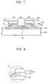
- FIG. 7 is a cross-sectional view illustrating the second metal layer corresponding to the first area and the semiconductor layer of which a portion is etched.
- the second metal layer 140 exposed by removing the photoresist film 201 of the first area 210 is etched, for example, by an etchant to form a source electrode 142 and a drain electrode 144 on the semiconductor layer 130 .
- the second metal layer 140 between the source electrode 142 and the drain electrode 144 is etched, the second semiconductor layer 134 corresponding to the first area 210 is exposed.
- the exposed second semiconductor layer 134 is etched by, for example, an etchant. In this process, a portion of the first semiconductor layer 132 may be etched. A portion ‘C’ of the remaining photoresist film 202 is lost while the second metal layer 140 and the second semiconductor layer 134 are etched.
- FIG. 8 is a partially enlarged view illustrating the portion ‘D’ illustrated in FIG. 7 .
- the first semiconductor layer 132 when a portion of the second semiconductor layer 134 and a portion of the first semiconductor layer 132 are etched, the first semiconductor layer 132 includes a protrusion ‘E’ protruding in a lateral direction. As the lost amount of the remaining photoresist film 202 is relatively small in an etching process, the protruding length of the protrusion ‘E’ the first semiconductor layer 132 is relatively small in comparison to when a positive photoresist film is used. Thus, the aperture ratio of a pixel is prevented from decreasing.
- FIG. 9 is a cross-sectional view illustrating the substrate wherein the remaining photoresist film is completely removed.
- the remaining photoresist film 202 is completely removed through an ashing process using oxygen plasma.
- the semiconductor layer 130 is hardly etched, as the etching selectivity of the semiconductor layer 130 is large with respect to the oxygen plasma.
- the TFT substrate is completely formed.
- a protecting layer may be formed on the substrate 100 to cover the source electrode 142 and the drain electrode 144 .
- a contact hole may be formed at the protecting layer corresponding to the drain electrode 144 through an exposure process and a developing process.
- a third metal layer may be formed on the protecting layer.
- the third metal layer may serve as a pixel electrode in the TFT substrate and be electrically connected to the drain electrode via the contact hole.
- the method of manufacturing a TFT substrate according to an exemplary embodiment of the present invention forms a negative photoresist film using a negative photoresist composition including a dye
- the method of manufacturing a TFT substrate may stably form a TFT substrate while also having the benefits associated with using negative photoresist films.
- a negative photoresist film formed using the photoresist composition of the exemplary embodiments of the present invention has a relatively large taper angle so that the lost amount of the negative photoresist film in an etching process is relatively small in comparison with a positive photoresist film.
- the protruding length of a semiconductor layer is reduced so that the aperture ratio of a pixel is prevented from decreasing.
- the photoresist composition of the exemplary embodiments of the present invention reduces the contrast of a negative photoresist film to stably form a halftone photoresist film. Also, a four-mask process using the photoresist composition may stably form a TFT substrate.
- a photoresist composition in accordance with exemplary embodiments of the present invention is also beneficial with respect to heat resistance and developing characteristics.
- the method of manufacturing a TFT substrate of exemplary embodiments of the present invention also increases the residual uniformity of a photoresist film between a source electrode and a drain electrode to prevent a short circuit and a pixel defect.
Landscapes
- Physics & Mathematics (AREA)
- Spectroscopy & Molecular Physics (AREA)
- General Physics & Mathematics (AREA)
- Engineering & Computer Science (AREA)
- Architecture (AREA)
- Structural Engineering (AREA)
- Materials For Photolithography (AREA)
- Exposure And Positioning Against Photoresist Photosensitive Materials (AREA)
- Thin Film Transistor (AREA)
- Photosensitive Polymer And Photoresist Processing (AREA)
- Heterocyclic Carbon Compounds Containing A Hetero Ring Having Oxygen Or Sulfur (AREA)
Abstract
Description


wherein R represents a halogen atom, an alkyl group having 1 to 5 carbon atoms, a cyclohexyl group, a bicyclohexyl group, a phenyl group, a biphenyl group, an alkylene group having 1 to 5 carbon atoms. The cyclohexyl group, the bicyclohexyl group, the phenyl group and the biphenyl group may each include an alcoxy group substituent. The alkylene group may include an alcoxy group having 1 to 5 carbon atoms, a nitrile halogen, a hydroxyl group, a hydrogen atom, as a substituent. Furthermore, the alkylene group may include a phenyl group substituent including an alkyl group having 1 to 5 carbon atoms, a nitrile group, a halogen atom, or a hydrogen atom as a substituent.
| TABLE 1 | ||||||
| Exam- | Exam- | Exam- | Comparative | |||
| ple 1 | ple 2 | ple 3 | Example 4 | Example | ||
| Sensitivity | 20 | 22 | 15 | 12 | 15 |
| (mj/cm2) | |||||
| Developing | 30 | 25 | 23 | 21 | 20 |
| Speed (sec) | |||||
| |
130 | 135 | 140 | 145 | 130 |
| Temperature | |||||
| (° C.) | |||||
| Contrast (λ) | 1.5 | 1.2 | 0.8 | 0.57 | 5.0 |
| Angle of Edge | 88 | 95 | 105 | 110 | 88 |
| Portion (°) | |||||
| Angle of Central | 55 | 60 | 63 | 67 | 55 |
| Portion (°) | |||||

Claims (30)


Applications Claiming Priority (2)
| Application Number | Priority Date | Filing Date | Title |
|---|---|---|---|
| KR1020050077308A KR101298940B1 (en) | 2005-08-23 | 2005-08-23 | Photoresist composition and method of manufacturing thin film transistor substrate using the same |
| KR2005-77308 | 2005-08-23 |
Publications (2)
| Publication Number | Publication Date |
|---|---|
| US20070048662A1 US20070048662A1 (en) | 2007-03-01 |
| US7595143B2 true US7595143B2 (en) | 2009-09-29 |
Family
ID=37804631
Family Applications (1)
| Application Number | Title | Priority Date | Filing Date |
|---|---|---|---|
| US11/508,079 Expired - Fee Related US7595143B2 (en) | 2005-08-23 | 2006-08-22 | Photoresist composition and method of manufacturing a thin-film transistor substrate using the same |
Country Status (5)
| Country | Link |
|---|---|
| US (1) | US7595143B2 (en) |
| JP (1) | JP4964534B2 (en) |
| KR (1) | KR101298940B1 (en) |
| CN (1) | CN1936705B (en) |
| TW (1) | TWI470344B (en) |
Cited By (10)
| Publication number | Priority date | Publication date | Assignee | Title |
|---|---|---|---|---|
| US20090002591A1 (en) * | 2007-06-29 | 2009-01-01 | Semiconductor Energy Laboratory Co., Ltd. | Liquid crystal display device |
| US20090001375A1 (en) * | 2007-06-29 | 2009-01-01 | Semiconductor Energy Laboratory Co., Ltd. | Light-emitting device |
| US8624237B2 (en) | 2008-07-31 | 2014-01-07 | Semiconductor Energy Laboratory Co., Ltd. | Semiconductor device and method for manufacturing the same |
| US8842230B2 (en) | 2007-07-06 | 2014-09-23 | Semiconductor Energy Laboratory Co., Ltd. | Liquid crystal display device |
| US8980685B2 (en) | 2008-10-24 | 2015-03-17 | Semiconductor Energy Laboratory Co., Ltd. | Method for manufacturing thin film transistor using multi-tone mask |
| US9660092B2 (en) | 2011-08-31 | 2017-05-23 | Semiconductor Energy Laboratory Co., Ltd. | Oxide semiconductor thin film transistor including oxygen release layer |
| US9766542B2 (en) | 2013-07-03 | 2017-09-19 | Kempur Microelectronics, Inc. | Negative chemically-amplified photoresist and imaging method thereof |
| US10256349B2 (en) | 2008-09-01 | 2019-04-09 | Semiconductor Energy Laboratory Co., Ltd. | Semiconductor device and method for manufacturing the semiconductor device |
| US10332996B2 (en) | 2009-12-04 | 2019-06-25 | Semiconductor Energy Laboratory Co., Ltd. | Semiconductor device and manufacturing method thereof |
| US10937897B2 (en) | 2008-07-31 | 2021-03-02 | Semiconductor Energy Laboratory Co., Ltd. | Semiconductor device and method for manufacturing the same |
Families Citing this family (25)
| Publication number | Priority date | Publication date | Assignee | Title |
|---|---|---|---|---|
| JP4850582B2 (en) * | 2006-05-24 | 2012-01-11 | 住友化学株式会社 | Colored photosensitive resin composition, color filter, image sensor and camera system |
| KR100849190B1 (en) * | 2007-03-19 | 2008-07-30 | 주식회사 하이닉스반도체 | Method of forming fine pattern of semiconductor device |
| KR101385946B1 (en) * | 2007-04-02 | 2014-04-16 | 주식회사 동진쎄미켐 | Photoresist composition and method of forming photoresist pattern using the same |
| KR101392291B1 (en) * | 2007-04-13 | 2014-05-07 | 주식회사 동진쎄미켐 | Photoresist composition and method of manufacturing a thin-film transistor substrate using the same |
| KR20080107314A (en) * | 2007-06-06 | 2008-12-10 | 후지필름 가부시키가이샤 | Thin metal film material and manufacturing method thereof |
| US8334537B2 (en) * | 2007-07-06 | 2012-12-18 | Semiconductor Energy Laboratory Co., Ltd. | Light-emitting device |
| US8786793B2 (en) * | 2007-07-27 | 2014-07-22 | Semiconductor Energy Laboratory Co., Ltd. | Display device and manufacturing method thereof |
| TWI605509B (en) * | 2007-09-03 | 2017-11-11 | 半導體能源研究所股份有限公司 | Thin film transistor and method of manufacturing display device |
| KR101523353B1 (en) * | 2007-12-03 | 2015-05-27 | 가부시키가이샤 한도오따이 에네루기 켄큐쇼 | Thin film transistor and semiconductor device |
| US8492459B2 (en) * | 2007-12-13 | 2013-07-23 | Lg Display Co., Ltd. | Ink composition and method of forming a pattern using the same |
| JP5336793B2 (en) * | 2008-08-29 | 2013-11-06 | 富士フイルム株式会社 | Pattern forming body manufacturing method and electromagnetic beam processing apparatus |
| US9082857B2 (en) * | 2008-09-01 | 2015-07-14 | Semiconductor Energy Laboratory Co., Ltd. | Semiconductor device comprising an oxide semiconductor layer |
| US8741702B2 (en) * | 2008-10-24 | 2014-06-03 | Semiconductor Energy Laboratory Co., Ltd. | Method for manufacturing semiconductor device |
| EP2180518B1 (en) * | 2008-10-24 | 2018-04-25 | Semiconductor Energy Laboratory Co, Ltd. | Method for manufacturing semiconductor device |
| WO2010047288A1 (en) * | 2008-10-24 | 2010-04-29 | Semiconductor Energy Laboratory Co., Ltd. | Method for manufacturing semiconductordevice |
| TWI490199B (en) * | 2009-03-11 | 2015-07-01 | Sumitomo Chemical Co | Compound and chemically amplified positive photoresist composition |
| US20110207527A1 (en) * | 2009-08-21 | 2011-08-25 | Aristocrat Technologies Australia Pty Limited | Method of gaming, a game controller and a gaming system |
| CN101907946A (en) * | 2010-08-13 | 2010-12-08 | 牧东光电(苏州)有限公司 | Method for externally expanding single edge of circuit of touch panel |
| US8536571B2 (en) * | 2011-01-12 | 2013-09-17 | Semiconductor Energy Laboratory Co., Ltd. | Manufacturing method of semiconductor device |
| TWI421638B (en) * | 2011-05-11 | 2014-01-01 | Chi Mei Corp | Positive photosensitive resin composition and method for forming patterns by using the same |
| US8932945B2 (en) * | 2012-07-09 | 2015-01-13 | Taiwan Semiconductor Manufacturing Company, Ltd. | Wafer alignment system and method |
| CN103809378A (en) * | 2014-01-26 | 2014-05-21 | 京东方科技集团股份有限公司 | Negative photoresist as well as preparation method and application method thereof |
| CN105742238A (en) * | 2016-03-02 | 2016-07-06 | 京东方科技集团股份有限公司 | Pore structure and array substrate, manufacturing methods of pore structure and array substrate, detection device and display device |
| KR102540963B1 (en) * | 2017-12-27 | 2023-06-07 | 삼성전자주식회사 | Method of forming a micropattern and substrate processing apparatus |
| CN108417583B (en) * | 2018-03-09 | 2021-10-29 | 惠科股份有限公司 | Method for manufacturing an array substrate and array substrate |
Citations (9)
| Publication number | Priority date | Publication date | Assignee | Title |
|---|---|---|---|---|
| US5731110A (en) * | 1993-02-02 | 1998-03-24 | Sumitomo Chemical Company, Limited | Photoresist composition for use in color filters |
| US6335276B1 (en) * | 1998-11-26 | 2002-01-01 | Samsung Electronics Co., Ltd. | Method for manufacturing a thin film transistor array panel for a liquid crystal display and a photolithography method for fabricating thin films |
| US6576394B1 (en) * | 2000-06-16 | 2003-06-10 | Clariant Finance (Bvi) Limited | Negative-acting chemically amplified photoresist composition |
| US6762802B2 (en) * | 2000-05-12 | 2004-07-13 | Renesas Technology Corp. | Liquid crystal display device and fabrication method thereof |
| US6872514B2 (en) * | 2002-03-25 | 2005-03-29 | Shin-Etsu Chemical Co., Ltd. | Polymers, resist compositions and patterning process |
| US7026091B2 (en) * | 2003-07-22 | 2006-04-11 | Industrial Technology Research Institute | Positive photoresist composition and patterning process using the same |
| US7291439B2 (en) * | 2005-07-08 | 2007-11-06 | Samsung Electronics Co., Ltd. | Photoresist composition, method for forming film pattern using the same, and method for manufacturing thin film transistor array panel using the same |
| US7297452B2 (en) * | 2004-12-24 | 2007-11-20 | Samsung Electronics Co., Ltd. | Photosensitive resin composition, thin film panel made with photosensitive composition, and method for manufacturing thin film panel |
| US7338737B2 (en) * | 2004-12-16 | 2008-03-04 | Samsung Electronics Co., Ltd. | Photosensitive resin composition, thin film panel made with photosensitive resin composition, and method for manufacturing thin film panel |
Family Cites Families (9)
| Publication number | Priority date | Publication date | Assignee | Title |
|---|---|---|---|---|
| JPH0736179A (en) * | 1993-07-19 | 1995-02-07 | Tokyo Ohka Kogyo Co Ltd | Negative photosensitive resin composition |
| JPH10228109A (en) * | 1997-02-14 | 1998-08-25 | Fuji Photo Film Co Ltd | Negative image recording material |
| JP2000258904A (en) * | 1999-03-04 | 2000-09-22 | Fujifilm Olin Co Ltd | Negative chemically amplified photosensitive composition |
| US6678018B2 (en) * | 2000-02-10 | 2004-01-13 | Samsung Electronics Co., Ltd. | Thin film transistor array substrate for a liquid crystal display and the method for fabricating the same |
| KR100869458B1 (en) * | 2000-02-21 | 2008-11-19 | 제온 코포레이션 | Resist composition |
| JP4370668B2 (en) * | 2000-03-29 | 2009-11-25 | Jsr株式会社 | Positive-type radiation-sensitive resin composition for plating model production and method for producing plating model |
| JP4401033B2 (en) * | 2001-03-19 | 2010-01-20 | Azエレクトロニックマテリアルズ株式会社 | Negative photosensitive resin composition and display device using the same |
| KR100947525B1 (en) * | 2003-03-12 | 2010-03-12 | 삼성전자주식회사 | Thin film transistor substrate for liquid crystal display device and manufacturing method thereof |
| JP4522660B2 (en) * | 2003-03-14 | 2010-08-11 | シャープ株式会社 | Method for manufacturing thin film transistor substrate |
-
2005
- 2005-08-23 KR KR1020050077308A patent/KR101298940B1/en not_active Expired - Fee Related
-
2006
- 2006-08-22 US US11/508,079 patent/US7595143B2/en not_active Expired - Fee Related
- 2006-08-22 JP JP2006224979A patent/JP4964534B2/en active Active
- 2006-08-23 CN CN2006101447713A patent/CN1936705B/en not_active Expired - Fee Related
- 2006-08-23 TW TW95130994A patent/TWI470344B/en not_active IP Right Cessation
Patent Citations (9)
| Publication number | Priority date | Publication date | Assignee | Title |
|---|---|---|---|---|
| US5731110A (en) * | 1993-02-02 | 1998-03-24 | Sumitomo Chemical Company, Limited | Photoresist composition for use in color filters |
| US6335276B1 (en) * | 1998-11-26 | 2002-01-01 | Samsung Electronics Co., Ltd. | Method for manufacturing a thin film transistor array panel for a liquid crystal display and a photolithography method for fabricating thin films |
| US6762802B2 (en) * | 2000-05-12 | 2004-07-13 | Renesas Technology Corp. | Liquid crystal display device and fabrication method thereof |
| US6576394B1 (en) * | 2000-06-16 | 2003-06-10 | Clariant Finance (Bvi) Limited | Negative-acting chemically amplified photoresist composition |
| US6872514B2 (en) * | 2002-03-25 | 2005-03-29 | Shin-Etsu Chemical Co., Ltd. | Polymers, resist compositions and patterning process |
| US7026091B2 (en) * | 2003-07-22 | 2006-04-11 | Industrial Technology Research Institute | Positive photoresist composition and patterning process using the same |
| US7338737B2 (en) * | 2004-12-16 | 2008-03-04 | Samsung Electronics Co., Ltd. | Photosensitive resin composition, thin film panel made with photosensitive resin composition, and method for manufacturing thin film panel |
| US7297452B2 (en) * | 2004-12-24 | 2007-11-20 | Samsung Electronics Co., Ltd. | Photosensitive resin composition, thin film panel made with photosensitive composition, and method for manufacturing thin film panel |
| US7291439B2 (en) * | 2005-07-08 | 2007-11-06 | Samsung Electronics Co., Ltd. | Photoresist composition, method for forming film pattern using the same, and method for manufacturing thin film transistor array panel using the same |
Cited By (27)
| Publication number | Priority date | Publication date | Assignee | Title |
|---|---|---|---|---|
| US20090002591A1 (en) * | 2007-06-29 | 2009-01-01 | Semiconductor Energy Laboratory Co., Ltd. | Liquid crystal display device |
| US20090001375A1 (en) * | 2007-06-29 | 2009-01-01 | Semiconductor Energy Laboratory Co., Ltd. | Light-emitting device |
| US8921858B2 (en) | 2007-06-29 | 2014-12-30 | Semiconductor Energy Laboratory Co., Ltd. | Light-emitting device |
| US9176353B2 (en) | 2007-06-29 | 2015-11-03 | Semiconductor Energy Laboratory Co., Ltd. | Liquid crystal display device |
| US12066730B2 (en) * | 2007-07-06 | 2024-08-20 | Semiconductor Energy Laboratory Co., Ltd. | Liquid crystal display device |
| US8842230B2 (en) | 2007-07-06 | 2014-09-23 | Semiconductor Energy Laboratory Co., Ltd. | Liquid crystal display device |
| US11726378B2 (en) | 2007-07-06 | 2023-08-15 | Semiconductor Energy Laboratory Co., Ltd. | Liquid crystal display device |
| US9188825B2 (en) | 2007-07-06 | 2015-11-17 | Semiconductor Energy Laboratory Co., Ltd. | Liquid crystal display device |
| US11194207B2 (en) | 2007-07-06 | 2021-12-07 | Semiconductor Energy Laboratory Co., Ltd. | Liquid crystal display device |
| US10338447B2 (en) | 2007-07-06 | 2019-07-02 | Semiconductor Energy Laboratory Co., Ltd. | Liquid crystal display device |
| US9766526B2 (en) | 2007-07-06 | 2017-09-19 | Semiconductor Energy Laboratory Co., Ltd. | Liquid crystal display device |
| US10712625B2 (en) | 2007-07-06 | 2020-07-14 | Semiconductor Energy Laboratory Co., Ltd. | Liquid crystal display device |
| US10678107B2 (en) | 2007-07-06 | 2020-06-09 | Semiconductor Energy Laboratory Co., Ltd. | Liquid crystal display device |
| US10937897B2 (en) | 2008-07-31 | 2021-03-02 | Semiconductor Energy Laboratory Co., Ltd. | Semiconductor device and method for manufacturing the same |
| US9496406B2 (en) | 2008-07-31 | 2016-11-15 | Semiconductor Energy Laboratory Co., Ltd. | Semiconductor device and method for manufacturing the same |
| US12074210B2 (en) | 2008-07-31 | 2024-08-27 | Semiconductor Energy Laboratory Co., Ltd. | Semiconductor device and method for manufacturing the same |
| US8624237B2 (en) | 2008-07-31 | 2014-01-07 | Semiconductor Energy Laboratory Co., Ltd. | Semiconductor device and method for manufacturing the same |
| US12068329B2 (en) | 2008-07-31 | 2024-08-20 | Semiconductor Energy Laboratory Co., Ltd. | Semiconductor device and method for manufacturing the same |
| US11296121B2 (en) | 2008-07-31 | 2022-04-05 | Semiconductor Energy Laboratory Co., Ltd. | Semiconductor device and method for manufacturing the same |
| US11201249B2 (en) | 2008-09-01 | 2021-12-14 | Semiconductor Energy Laboratory Co., Ltd. | Liquid crystal display device comprising an oxide semiconductor |
| US11824124B2 (en) | 2008-09-01 | 2023-11-21 | Semiconductor Energy Laboratory Co., Ltd. | Liquid crystal display device including transistor comprising oxide semiconductor |
| US10734530B2 (en) | 2008-09-01 | 2020-08-04 | Semiconductor Energy Laboratory Co., Ltd. | Semiconductor device comprising oxide semiconductor |
| US10256349B2 (en) | 2008-09-01 | 2019-04-09 | Semiconductor Energy Laboratory Co., Ltd. | Semiconductor device and method for manufacturing the semiconductor device |
| US8980685B2 (en) | 2008-10-24 | 2015-03-17 | Semiconductor Energy Laboratory Co., Ltd. | Method for manufacturing thin film transistor using multi-tone mask |
| US10332996B2 (en) | 2009-12-04 | 2019-06-25 | Semiconductor Energy Laboratory Co., Ltd. | Semiconductor device and manufacturing method thereof |
| US9660092B2 (en) | 2011-08-31 | 2017-05-23 | Semiconductor Energy Laboratory Co., Ltd. | Oxide semiconductor thin film transistor including oxygen release layer |
| US9766542B2 (en) | 2013-07-03 | 2017-09-19 | Kempur Microelectronics, Inc. | Negative chemically-amplified photoresist and imaging method thereof |
Also Published As
| Publication number | Publication date |
|---|---|
| TW200722910A (en) | 2007-06-16 |
| JP4964534B2 (en) | 2012-07-04 |
| JP2007058216A (en) | 2007-03-08 |
| KR20070023103A (en) | 2007-02-28 |
| TWI470344B (en) | 2015-01-21 |
| CN1936705A (en) | 2007-03-28 |
| KR101298940B1 (en) | 2013-08-22 |
| CN1936705B (en) | 2011-12-21 |
| US20070048662A1 (en) | 2007-03-01 |
Similar Documents
| Publication | Publication Date | Title |
|---|---|---|
| US7595143B2 (en) | Photoresist composition and method of manufacturing a thin-film transistor substrate using the same | |
| KR101392291B1 (en) | Photoresist composition and method of manufacturing a thin-film transistor substrate using the same | |
| US9366959B2 (en) | Negative photosensitive resin composition and application thereof | |
| KR101415545B1 (en) | Alkali soluble polymer and positive working photosensitive resin composition using the same | |
| KR20090109432A (en) | Photosensitive resin, the formation method of the pattern using the said photosensitive resin, and the manufacturing method of a display panel | |
| US20110294243A1 (en) | Photoresist composition and method of forming photoresist pattern using the same | |
| CN101236356A (en) | Photoresist composition, method of patterning thin film and method of making liquid crystal display panel | |
| US20070003860A1 (en) | Substrate adhesion improver for photosensitive resin composition and photosensitive resin composition containing the same | |
| KR101430962B1 (en) | Photoresist composition and method for manufacturing array substrate using the same | |
| US20230037563A1 (en) | Metal containing photoresist developer composition, and method of forming patterns including developing step using the same | |
| KR100585301B1 (en) | Chemical amplified type positive resist composition for liquid crystal element | |
| US20250123568A1 (en) | Composition for removing edge bead from metal containing resists, developer composition of metal containing resists, and method of forming patterns using the composition | |
| KR101034347B1 (en) | Photosensitive resin composition | |
| US8808963B2 (en) | Photoresist composition and method of manufacturing array substrate using the same | |
| KR20070066445A (en) | Manufacturing Method of Display Board | |
| KR101564403B1 (en) | Method of fabricating thin film transistor substrate and negative photoresist composition used therein | |
| KR20090040584A (en) | A photosensitive resin composition and a liquid crystal display device produced thereby. | |
| JP4446181B2 (en) | Pattern formation method | |
| KR101205471B1 (en) | Photosensitive resin composition for tft-lcd | |
| CN116880125A (en) | Positive photosensitive resin composition, use thereof, and metal patterning method using the same | |
| KR20070008924A (en) | Manufacturing method of field forming electrode and manufacturing method of liquid crystal display device using same | |
| JP2007272002A (en) | Resist pattern forming method and photosensitive resin composition |
Legal Events
| Date | Code | Title | Description |
|---|---|---|---|
| AS | Assignment |
Owner name: SAMSUNG ELECTRONICS CO., LTD., KOREA, REPUBLIC OF Free format text: ASSIGNMENT OF ASSIGNORS INTEREST;ASSIGNORS:PARK, JEONG-MIN;LEE, HI-KUK;YOUN, HYOC-MIN;AND OTHERS;REEL/FRAME:018222/0494;SIGNING DATES FROM 20060802 TO 20060817 |
|
| STCF | Information on status: patent grant |
Free format text: PATENTED CASE |
|
| FEPP | Fee payment procedure |
Free format text: PAYOR NUMBER ASSIGNED (ORIGINAL EVENT CODE: ASPN); ENTITY STATUS OF PATENT OWNER: LARGE ENTITY |
|
| AS | Assignment |
Owner name: SAMSUNG DISPLAY CO., LTD., KOREA, REPUBLIC OF Free format text: ASSIGNMENT OF ASSIGNORS INTEREST;ASSIGNOR:SAMSUNG ELECTRONICS CO., LTD.;REEL/FRAME:029045/0860 Effective date: 20120904 |
|
| FEPP | Fee payment procedure |
Free format text: PAYOR NUMBER ASSIGNED (ORIGINAL EVENT CODE: ASPN); ENTITY STATUS OF PATENT OWNER: LARGE ENTITY Free format text: PAYER NUMBER DE-ASSIGNED (ORIGINAL EVENT CODE: RMPN); ENTITY STATUS OF PATENT OWNER: LARGE ENTITY |
|
| FPAY | Fee payment |
Year of fee payment: 4 |
|
| FPAY | Fee payment |
Year of fee payment: 8 |
|
| FEPP | Fee payment procedure |
Free format text: MAINTENANCE FEE REMINDER MAILED (ORIGINAL EVENT CODE: REM.); ENTITY STATUS OF PATENT OWNER: LARGE ENTITY |
|
| LAPS | Lapse for failure to pay maintenance fees |
Free format text: PATENT EXPIRED FOR FAILURE TO PAY MAINTENANCE FEES (ORIGINAL EVENT CODE: EXP.); ENTITY STATUS OF PATENT OWNER: LARGE ENTITY |
|
| STCH | Information on status: patent discontinuation |
Free format text: PATENT EXPIRED DUE TO NONPAYMENT OF MAINTENANCE FEES UNDER 37 CFR 1.362 |
|
| FP | Lapsed due to failure to pay maintenance fee |
Effective date: 20210929 |