US7594968B2 - Ultratough CVD single crystal diamond and three dimensional growth thereof - Google Patents
Ultratough CVD single crystal diamond and three dimensional growth thereof Download PDFInfo
- Publication number
- US7594968B2 US7594968B2 US11/222,224 US22222405A US7594968B2 US 7594968 B2 US7594968 B2 US 7594968B2 US 22222405 A US22222405 A US 22222405A US 7594968 B2 US7594968 B2 US 7594968B2
- Authority
- US
- United States
- Prior art keywords
- diamond
- crystal diamond
- cvd
- diamonds
- single crystal
- Prior art date
- Legal status (The legal status is an assumption and is not a legal conclusion. Google has not performed a legal analysis and makes no representation as to the accuracy of the status listed.)
- Active, expires
Links
- 239000010432 diamond Substances 0.000 title claims abstract description 182
- 229910003460 diamond Inorganic materials 0.000 title claims abstract description 140
- 239000013078 crystal Substances 0.000 title claims abstract description 85
- 238000005229 chemical vapour deposition Methods 0.000 claims abstract description 61
- 238000005520 cutting process Methods 0.000 claims description 6
- 239000010437 gem Substances 0.000 claims description 6
- 230000003287 optical effect Effects 0.000 claims description 5
- 238000005491 wire drawing Methods 0.000 claims 1
- 238000000034 method Methods 0.000 abstract description 32
- 239000000758 substrate Substances 0.000 abstract description 28
- 230000008569 process Effects 0.000 abstract description 13
- IJGRMHOSHXDMSA-UHFFFAOYSA-N Atomic nitrogen Chemical compound N#N IJGRMHOSHXDMSA-UHFFFAOYSA-N 0.000 description 30
- 238000000137 annealing Methods 0.000 description 20
- VNWKTOKETHGBQD-UHFFFAOYSA-N methane Chemical compound C VNWKTOKETHGBQD-UHFFFAOYSA-N 0.000 description 19
- 229910052757 nitrogen Inorganic materials 0.000 description 16
- 238000007373 indentation Methods 0.000 description 13
- 238000000151 deposition Methods 0.000 description 7
- 230000008021 deposition Effects 0.000 description 7
- 230000007547 defect Effects 0.000 description 6
- 230000008901 benefit Effects 0.000 description 5
- 239000007789 gas Substances 0.000 description 5
- 239000000463 material Substances 0.000 description 5
- OKTJSMMVPCPJKN-UHFFFAOYSA-N Carbon Chemical compound [C] OKTJSMMVPCPJKN-UHFFFAOYSA-N 0.000 description 4
- UFHFLCQGNIYNRP-UHFFFAOYSA-N Hydrogen Chemical compound [H][H] UFHFLCQGNIYNRP-UHFFFAOYSA-N 0.000 description 4
- 238000010521 absorption reaction Methods 0.000 description 3
- 230000015572 biosynthetic process Effects 0.000 description 3
- 230000008859 change Effects 0.000 description 3
- 229910052739 hydrogen Inorganic materials 0.000 description 3
- 239000012535 impurity Substances 0.000 description 3
- 238000004519 manufacturing process Methods 0.000 description 3
- 238000005424 photoluminescence Methods 0.000 description 3
- 238000005033 Fourier transform infrared spectroscopy Methods 0.000 description 2
- 241000078511 Microtome Species 0.000 description 2
- 229910003481 amorphous carbon Inorganic materials 0.000 description 2
- 238000004458 analytical method Methods 0.000 description 2
- 229910052799 carbon Inorganic materials 0.000 description 2
- 239000011248 coating agent Substances 0.000 description 2
- 238000000576 coating method Methods 0.000 description 2
- 239000012530 fluid Substances 0.000 description 2
- 229910001751 gemstone Inorganic materials 0.000 description 2
- 229910002804 graphite Inorganic materials 0.000 description 2
- 239000010439 graphite Substances 0.000 description 2
- 239000001257 hydrogen Substances 0.000 description 2
- 238000011835 investigation Methods 0.000 description 2
- 230000007246 mechanism Effects 0.000 description 2
- 238000002844 melting Methods 0.000 description 2
- 230000008018 melting Effects 0.000 description 2
- 230000008439 repair process Effects 0.000 description 2
- 238000011160 research Methods 0.000 description 2
- 239000004065 semiconductor Substances 0.000 description 2
- 230000035939 shock Effects 0.000 description 2
- 238000003786 synthesis reaction Methods 0.000 description 2
- XLYOFNOQVPJJNP-UHFFFAOYSA-N water Substances O XLYOFNOQVPJJNP-UHFFFAOYSA-N 0.000 description 2
- ZOXJGFHDIHLPTG-UHFFFAOYSA-N Boron Chemical compound [B] ZOXJGFHDIHLPTG-UHFFFAOYSA-N 0.000 description 1
- 239000004215 Carbon black (E152) Substances 0.000 description 1
- 241000735235 Ligustrum vulgare Species 0.000 description 1
- 238000001069 Raman spectroscopy Methods 0.000 description 1
- 238000001237 Raman spectrum Methods 0.000 description 1
- 238000000429 assembly Methods 0.000 description 1
- 230000000712 assembly Effects 0.000 description 1
- 229910052796 boron Inorganic materials 0.000 description 1
- 238000004364 calculation method Methods 0.000 description 1
- 239000003086 colorant Substances 0.000 description 1
- 238000011109 contamination Methods 0.000 description 1
- 238000001816 cooling Methods 0.000 description 1
- 238000005336 cracking Methods 0.000 description 1
- 230000003247 decreasing effect Effects 0.000 description 1
- 239000002019 doping agent Substances 0.000 description 1
- 230000005670 electromagnetic radiation Effects 0.000 description 1
- 230000005284 excitation Effects 0.000 description 1
- 229930195733 hydrocarbon Natural products 0.000 description 1
- 150000002430 hydrocarbons Chemical class 0.000 description 1
- 238000004631 ion microprobe analysis Methods 0.000 description 1
- 230000001788 irregular Effects 0.000 description 1
- 238000011031 large-scale manufacturing process Methods 0.000 description 1
- 229910052744 lithium Inorganic materials 0.000 description 1
- 229910052749 magnesium Inorganic materials 0.000 description 1
- 238000005259 measurement Methods 0.000 description 1
- 239000013080 microcrystalline material Substances 0.000 description 1
- 238000012986 modification Methods 0.000 description 1
- 230000004048 modification Effects 0.000 description 1
- 239000002159 nanocrystal Substances 0.000 description 1
- 239000002245 particle Substances 0.000 description 1
- 238000000103 photoluminescence spectrum Methods 0.000 description 1
- 239000000843 powder Substances 0.000 description 1
- 239000000126 substance Substances 0.000 description 1
- 239000002887 superconductor Substances 0.000 description 1
- 230000001131 transforming effect Effects 0.000 description 1
- UONOETXJSWQNOL-UHFFFAOYSA-N tungsten carbide Chemical compound [W+]#[C-] UONOETXJSWQNOL-UHFFFAOYSA-N 0.000 description 1
Images


Classifications
-
- C—CHEMISTRY; METALLURGY
- C30—CRYSTAL GROWTH
- C30B—SINGLE-CRYSTAL GROWTH; UNIDIRECTIONAL SOLIDIFICATION OF EUTECTIC MATERIAL OR UNIDIRECTIONAL DEMIXING OF EUTECTOID MATERIAL; REFINING BY ZONE-MELTING OF MATERIAL; PRODUCTION OF A HOMOGENEOUS POLYCRYSTALLINE MATERIAL WITH DEFINED STRUCTURE; SINGLE CRYSTALS OR HOMOGENEOUS POLYCRYSTALLINE MATERIAL WITH DEFINED STRUCTURE; AFTER-TREATMENT OF SINGLE CRYSTALS OR A HOMOGENEOUS POLYCRYSTALLINE MATERIAL WITH DEFINED STRUCTURE; APPARATUS THEREFOR
- C30B25/00—Single-crystal growth by chemical reaction of reactive gases, e.g. chemical vapour-deposition growth
- C30B25/02—Epitaxial-layer growth
- C30B25/10—Heating of the reaction chamber or the substrate
- C30B25/105—Heating of the reaction chamber or the substrate by irradiation or electric discharge
-
- C—CHEMISTRY; METALLURGY
- C23—COATING METALLIC MATERIAL; COATING MATERIAL WITH METALLIC MATERIAL; CHEMICAL SURFACE TREATMENT; DIFFUSION TREATMENT OF METALLIC MATERIAL; COATING BY VACUUM EVAPORATION, BY SPUTTERING, BY ION IMPLANTATION OR BY CHEMICAL VAPOUR DEPOSITION, IN GENERAL; INHIBITING CORROSION OF METALLIC MATERIAL OR INCRUSTATION IN GENERAL
- C23C—COATING METALLIC MATERIAL; COATING MATERIAL WITH METALLIC MATERIAL; SURFACE TREATMENT OF METALLIC MATERIAL BY DIFFUSION INTO THE SURFACE, BY CHEMICAL CONVERSION OR SUBSTITUTION; COATING BY VACUUM EVAPORATION, BY SPUTTERING, BY ION IMPLANTATION OR BY CHEMICAL VAPOUR DEPOSITION, IN GENERAL
- C23C16/00—Chemical coating by decomposition of gaseous compounds, without leaving reaction products of surface material in the coating, i.e. chemical vapour deposition [CVD] processes
- C23C16/22—Chemical coating by decomposition of gaseous compounds, without leaving reaction products of surface material in the coating, i.e. chemical vapour deposition [CVD] processes characterised by the deposition of inorganic material, other than metallic material
- C23C16/26—Deposition of carbon only
- C23C16/27—Diamond only
- C23C16/274—Diamond only using microwave discharges
-
- C—CHEMISTRY; METALLURGY
- C23—COATING METALLIC MATERIAL; COATING MATERIAL WITH METALLIC MATERIAL; CHEMICAL SURFACE TREATMENT; DIFFUSION TREATMENT OF METALLIC MATERIAL; COATING BY VACUUM EVAPORATION, BY SPUTTERING, BY ION IMPLANTATION OR BY CHEMICAL VAPOUR DEPOSITION, IN GENERAL; INHIBITING CORROSION OF METALLIC MATERIAL OR INCRUSTATION IN GENERAL
- C23C—COATING METALLIC MATERIAL; COATING MATERIAL WITH METALLIC MATERIAL; SURFACE TREATMENT OF METALLIC MATERIAL BY DIFFUSION INTO THE SURFACE, BY CHEMICAL CONVERSION OR SUBSTITUTION; COATING BY VACUUM EVAPORATION, BY SPUTTERING, BY ION IMPLANTATION OR BY CHEMICAL VAPOUR DEPOSITION, IN GENERAL
- C23C16/00—Chemical coating by decomposition of gaseous compounds, without leaving reaction products of surface material in the coating, i.e. chemical vapour deposition [CVD] processes
- C23C16/22—Chemical coating by decomposition of gaseous compounds, without leaving reaction products of surface material in the coating, i.e. chemical vapour deposition [CVD] processes characterised by the deposition of inorganic material, other than metallic material
- C23C16/26—Deposition of carbon only
- C23C16/27—Diamond only
- C23C16/277—Diamond only using other elements in the gas phase besides carbon and hydrogen; using other elements besides carbon, hydrogen and oxygen in case of use of combustion torches; using other elements besides carbon, hydrogen and inert gas in case of use of plasma jets
-
- C—CHEMISTRY; METALLURGY
- C23—COATING METALLIC MATERIAL; COATING MATERIAL WITH METALLIC MATERIAL; CHEMICAL SURFACE TREATMENT; DIFFUSION TREATMENT OF METALLIC MATERIAL; COATING BY VACUUM EVAPORATION, BY SPUTTERING, BY ION IMPLANTATION OR BY CHEMICAL VAPOUR DEPOSITION, IN GENERAL; INHIBITING CORROSION OF METALLIC MATERIAL OR INCRUSTATION IN GENERAL
- C23C—COATING METALLIC MATERIAL; COATING MATERIAL WITH METALLIC MATERIAL; SURFACE TREATMENT OF METALLIC MATERIAL BY DIFFUSION INTO THE SURFACE, BY CHEMICAL CONVERSION OR SUBSTITUTION; COATING BY VACUUM EVAPORATION, BY SPUTTERING, BY ION IMPLANTATION OR BY CHEMICAL VAPOUR DEPOSITION, IN GENERAL
- C23C16/00—Chemical coating by decomposition of gaseous compounds, without leaving reaction products of surface material in the coating, i.e. chemical vapour deposition [CVD] processes
- C23C16/22—Chemical coating by decomposition of gaseous compounds, without leaving reaction products of surface material in the coating, i.e. chemical vapour deposition [CVD] processes characterised by the deposition of inorganic material, other than metallic material
- C23C16/26—Deposition of carbon only
- C23C16/27—Diamond only
- C23C16/279—Diamond only control of diamond crystallography
-
- C—CHEMISTRY; METALLURGY
- C30—CRYSTAL GROWTH
- C30B—SINGLE-CRYSTAL GROWTH; UNIDIRECTIONAL SOLIDIFICATION OF EUTECTIC MATERIAL OR UNIDIRECTIONAL DEMIXING OF EUTECTOID MATERIAL; REFINING BY ZONE-MELTING OF MATERIAL; PRODUCTION OF A HOMOGENEOUS POLYCRYSTALLINE MATERIAL WITH DEFINED STRUCTURE; SINGLE CRYSTALS OR HOMOGENEOUS POLYCRYSTALLINE MATERIAL WITH DEFINED STRUCTURE; AFTER-TREATMENT OF SINGLE CRYSTALS OR A HOMOGENEOUS POLYCRYSTALLINE MATERIAL WITH DEFINED STRUCTURE; APPARATUS THEREFOR
- C30B23/00—Single-crystal growth by condensing evaporated or sublimed materials
-
- C—CHEMISTRY; METALLURGY
- C30—CRYSTAL GROWTH
- C30B—SINGLE-CRYSTAL GROWTH; UNIDIRECTIONAL SOLIDIFICATION OF EUTECTIC MATERIAL OR UNIDIRECTIONAL DEMIXING OF EUTECTOID MATERIAL; REFINING BY ZONE-MELTING OF MATERIAL; PRODUCTION OF A HOMOGENEOUS POLYCRYSTALLINE MATERIAL WITH DEFINED STRUCTURE; SINGLE CRYSTALS OR HOMOGENEOUS POLYCRYSTALLINE MATERIAL WITH DEFINED STRUCTURE; AFTER-TREATMENT OF SINGLE CRYSTALS OR A HOMOGENEOUS POLYCRYSTALLINE MATERIAL WITH DEFINED STRUCTURE; APPARATUS THEREFOR
- C30B28/00—Production of homogeneous polycrystalline material with defined structure
- C30B28/12—Production of homogeneous polycrystalline material with defined structure directly from the gas state
- C30B28/14—Production of homogeneous polycrystalline material with defined structure directly from the gas state by chemical reaction of reactive gases
-
- C—CHEMISTRY; METALLURGY
- C30—CRYSTAL GROWTH
- C30B—SINGLE-CRYSTAL GROWTH; UNIDIRECTIONAL SOLIDIFICATION OF EUTECTIC MATERIAL OR UNIDIRECTIONAL DEMIXING OF EUTECTOID MATERIAL; REFINING BY ZONE-MELTING OF MATERIAL; PRODUCTION OF A HOMOGENEOUS POLYCRYSTALLINE MATERIAL WITH DEFINED STRUCTURE; SINGLE CRYSTALS OR HOMOGENEOUS POLYCRYSTALLINE MATERIAL WITH DEFINED STRUCTURE; AFTER-TREATMENT OF SINGLE CRYSTALS OR A HOMOGENEOUS POLYCRYSTALLINE MATERIAL WITH DEFINED STRUCTURE; APPARATUS THEREFOR
- C30B29/00—Single crystals or homogeneous polycrystalline material with defined structure characterised by the material or by their shape
- C30B29/02—Elements
- C30B29/04—Diamond
Definitions
- the present invention relates to an annealed single-crystal CVD diamond having an extremely high toughness.
- the invention also relates to a process for producing a single-crystal CVD diamond in three dimensions on a single crystal diamond substrate using Microwave Plasma Chemical Vapor Deposition (MPCVD) within a deposition chamber.
- MPCVD Microwave Plasma Chemical Vapor Deposition
- Diamond in addition to its gem properties, is the hardest known material, has the highest known thermal conductivity, and is transparent to a wide variety of electromagnetic radiation.
- Monocrystalline diamond in particular possess a wide range of important properties, including a low coefficient of thermal expansion, the highest known thermal conductivity, chemical inertness, wear resistance, low friction, and optical transparency from the ultra-violet (UV) to the far infrared (IR). Therefore, it is valuable because of its wide range of applications in a number of industries and research applications, in addition to its value as a gemstone.
- SC-CVD single-crystal chemical vapor deposition
- U.S. Pat. No. 6,858,078 to Hemley et al. is directed to an apparatus and method for diamond production.
- the disclosed apparatus and method can lead to the production of diamonds that are light brown to colorless.
- U.S. patent application Ser. No. 10/889,171 is directed to annealing single-crystal chemical vapor deposition diamonds. Important inventive features include raising the CVD diamond to a set temperature of at least 1500° C. and a pressure of at least 4.0 GPa outside of the diamond stable phase.
- U.S. patent application Ser. No. 10/889,170 is directed to diamonds with improved hardness.
- the application discloses a single-crystal diamond with a hardness greater than 120 GPa.
- U.S. patent application Ser. No. 10/889,169 is directed to diamonds with improved toughness.
- the application discloses a single-crystal diamond with a fracture toughness of 11-20 MPam 1/2 and a hardness of 50-90 GPa.
- the present invention is directed to a single-crystal diamond and a method of producing such a diamond that substantially obviates one or more of the problems due to limitations and disadvantages of the related art.
- An object of the present invention relates to an ultratough diamond and a method of producing such a diamond in a microwave plasma chemical vapor deposition system. Another object of the present invention relates to a method to produce single-crystal diamond with growth in three dimensions on a single crystal diamond substrate.
- an embodiment of the invention comprises a single-crystal diamond grown by microwave plasma chemical vapor deposition that has a toughness of at least about 30 MPa m 1/2 .
- Another embodiment of the invention relates to a method for growing an ultratough, single-crystal diamond comprising:
- Another embodiment of the invention relates to a process for producing a single crystal CVD diamond in three dimensions on a single crystal diamond substrate, comprising:
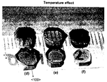
- FIG. 1 provides photographs of CVD and aCVD diamonds grown under different conditions.
- FIG. 2 depicts indentation patterns for various CVD and aCVD diamonds.
- FIG. 3 is a photoluminescence spectra of various CVD and aCVD diamonds.
- FIG. 4 shows infrared absorption (FTIR) data for various CVD and aCVD diamonds.
- One embodiment of the invention includes a single-crystal diamond grown by microwave plasma chemical vapor deposition that has a toughness of at least about 30 MPa m 1/2 . In another embodiment, the toughness of the single-crystal diamond is at least about 35 MPa m 1/2 . In another embodiment, the toughness of the single-crystal diamond is at least about 40 MPa m 1/2 .
- the diamonds in these embodiments of the invention were subjected to annealing, for example, at temperatures of about 2000° C. to about 2700° C. for about 10 minutes using a belt-type apparatus. This caused a dramatic increase in the hardness of the diamonds. In another embodiment, the hardness is from about 100 to about 160 GPa.
- Another embodiment includes a method for growing an ultratough, single-crystal diamond comprising:
- the aforementioned method further comprises annealing the single-crystal diamond at pressures in excess of about 5 to about 7 GPa and temperatures of from about 2000° C. to about 2700° C. such that the hardness is from about 100 to about 160 GPa.
- the single crystal diamond prior to annealing is substantially colorless.
- Another embodiment of the invention includes a process for producing a single crystal CVD diamond in three dimensions on a single crystal diamond substrate, comprising:
- the color change is achieved by placing the Ib diamond on a substrate holder with only modest thermal conductivity (e.g., hBN powder or Mo wires to hold the substrate).
- the color change appears similar to that reported for natural diamond on HPHT annealing. See I. M. Reinitz, et al., Gems & Gemology (2000) 36, 128.
- CVD diamond did not undergo obvious color changes and transformed to graphite at temperatures above 1800° C. in the same process. It was therefore of interest to anneal CVD diamond at higher temperature over 2000° C. by High Pressure/High Temperature (HPHT) methods.
- HPHT High Pressure/High Temperature
- Single crystal diamonds were synthesized by microwave plasma chemical vapor deposition (CVD) at 8-20% CH 4 /H 2 , 0.2-3% N 2 /CH 4 , 160-220 torr at various temperatures.
- the diamonds shown in FIG. 1 were grown at the following temperatures: (a) 1300° C.; (b) 1250° C.; (c) 1400° C.; (d) 1200° C.; (e) 1050° C.
- Diamond (f) is the type Ib diamond substrate (4 ⁇ 4 ⁇ 1.5 mm 3 ). All substrates were HPHT synthetic type Ib yellow diamonds with ⁇ 100 ⁇ faces on top and on the sides. Morphologies and colors of the as-grown CVD diamonds strongly depend on the deposition temperature.
- the top growth surface of the sample has been enlarged by a factor of two relative to the substrate [ FIG. 1( d )], whereas the shape of the sample in FIG. 1( a ) remains similar.
- colorless CVD diamond with nitrogen added can be enlarged along three ⁇ 100> directions at deposition temperatures around 1200° C.
- Such three-dimensional enlargement of the structures at around 1200° C. is important for continued growth to produce gem-quality diamond with much larger lateral dimensions than the substrates.
- gem-quality CVD diamond can be grown individually and sequentially on the 6 ⁇ 100 ⁇ faces of the substrate. By this method, a one inch cube of single crystal diamond ( ⁇ 300 carat) is achievable.
- FIG. 2( a ) shows the indentation pattern of Natural IIa diamond that has a hardness of approximately 110 GPa.
- FIG. 2( b ) shows the indentation pattern of annealed IIa diamond with a hardness of approximately 140 GPa.
- FIG. 2( c ) shows the indentation pattern of unannealed CVD diamond with a hardness of about 60 GPa.
- FIG. 2( d ) shows the indentation pattern of annealed, colorless, ultrahard aCVD diamond grown under low nitrogen conditions, which has a hardness of about 160 GPa.
- FIG. 2( a ) shows the indentation pattern of Natural IIa diamond that has a hardness of approximately 110 GPa.
- FIG. 2( b ) shows the indentation pattern of annealed IIa diamond with a hardness of approximately 140 GPa.
- FIG. 2( c ) shows the indentation pattern of unannealed CVD diamond with a hardness
- FIG. 2( e ) shows the indentation pattern of ultrahard aCVD diamond grown under high nitrogen conditions, which has a hardness of about 160 GPa.
- FIG. 2( f ) shows the indentation pattern of colorless, ultratough aCVD diamond grown under high nitrogen conditions, with a hardness of from about 100 to about 160 GPa.
- the circular indentation patterns seen after annealing in the colorless diamonds grown at low nitrogen/methane ratio (about 0.4% N 2 /CH 4 ) and about 1200° C. ( FIG. 2( d )) are similar to those of annealed natural type IIa diamonds ( FIG. 2( b )).
- FIG. 3 shows Photoluminescence (PL) and Raman spectra that were measured with 488 nm excitation.
- CVD diamonds showed an obvious nitrogen-vacancy (N-V) center at 575 nm; the intensity of this band is higher for the brown relative to the colorless CVD diamonds.
- N-V nitrogen-vacancy
- the as-grown brown CVD diamond that had been annealed to colorless possesses a strong nitrogen aggregate (H3) center (see S. J. Charles et al., (2004) Physica Status Solidi (a): 1-13) at 503 nm with a decrease in the band associated with the N-V center. Note that the H3 peak is strongest for the unindented (ultrahard) diamond.
- the annealed as-grown colorless CVD diamond possesses both H3 and N-V centers, but the intensities of these bands decreased by two orders after annealing, and the second-order Raman band of diamond appeared.
- the N-V centers in the annealed CVD may imply vacancy-rich CVD transforms to denser structures after HPHT annealing.
- FIG. 4 shows the C—H stretching of infrared absorption in the range of 2800-3200 cm ⁇ 1 .
- the broad band at 2930 cm ⁇ 1 attributed to hydrogenated amorphous carbon (a-C:H) is observed in the brown CVD diamond. This intensity correlates with the brown color of the diamond and its high toughness.
- the a-C:H peak was annealed to various well-resolved C—H stretching bands at 2830 cm ⁇ 1 (sp 3 ⁇ 111 ⁇ defects), 2875 (sp 3 -CH 3 defects), and 2900 cm ⁇ 1 (sp 3 ⁇ 100 ⁇ defects) as well as 2972, 3032 and 3107 cm ⁇ 1 (sp 2 defects) (see K. M.
- the ⁇ 111 ⁇ surfaces within the aCVD implies the relatively open a-C:H structure in the as-grown ⁇ 100 ⁇ CVD transformed on annealing to locally denser structure. For example, there is an increase in internal ⁇ 111 ⁇ defects and sp 2 carbon on the boundary. This change may contribute to the square ⁇ 111> or ⁇ 110> indented pattern in FIG. 2 .
- the colorless CVD diamond has lower intensity bands associated with a-C:H exhibited a broad and intense band at 2800 cm ⁇ 1 . This feature could be associated with unintentional contamination of boron (see Z.
- FWHM full width at half-maximum
- brown CVD is ⁇ 80 arcsec
- aCVD is ⁇ 150-300 arcsec.
- the mechanism of the very high fracture toughness documented here may be associated with the small amount of amorphous carbon or dislocations that exist in these single-crystal CVD diamonds. Denser sp 2 or sp 3 hybridized nanocrystals combined with changes in nitrogen and hydrogen impurities on their grain boundary may occur during HPHT annealing.
- the ultratough diamonds of the invention and diamonds produced by the above methods will be sufficiently large, tough, defect free and translucent so as to be useful as, for example, windows in high power laser or synchrotron applications, as anvils in high pressure apparatuses, as cutting instruments, as wire dies, as components for electronics (heat sinks, substrates for electronic devices), or as gems.
- Other examples of uses or applications for the above ultratough diamonds and diamonds made by the above methods include the following:
- the ultratough diamonds disclosed herein are particularly useful in applications, including, but not limited to, water/fluid jet nozzles, razors, surgical blades, microtone, hardness indentor, graphical tools, stichels, instruments used in the repair of lithographic pieces, missile radomes, bearings, including those used in ultra-high speed machines, diamond-biomolecule devices, microtomes, hardness indentors, and anvils in high pressure apparatuses.
- the present invention is directed to anvils in high pressure apparatuses, wherein the anvils comprise ultratough single-crystal CVD diamond.
- Anvils comprising ultratough single-crystal CVD diamond can be used at higher pressures than anvils made of other materials, such as tungsten carbide.
- Examples of anvil designs that can comprise single crystal CVD diamonds include Bridgman anvils, including, but not limited to, Bridgman anvils that are relatively large, include variable heights, and include major angles and Paris-Edinburgh toroid anvils, including, but not limited to, those discussed in Khvostantsev, L. G., Vereshchagin, L. F., and Novikov, A. P., Device of toroid type for high pressure generation, High Temperatures-High Pressures, 1977, vol. 9, pp 637-638.
- the present invention is directed to an ultratough single-crystal CVD diamond that is laser inscribed with identifying marks (e.g., name, date, number) and a method of preparing such a diamond.
- identifying marks e.g., name, date, number
- the identifying marks can be laser inscribed onto a diamond substrate prior to starting the CVD process to prepare a single-crystal diamond.
- the mark is transferred to the single-crystal diamond through this process.
Landscapes
- Chemical & Material Sciences (AREA)
- Engineering & Computer Science (AREA)
- Organic Chemistry (AREA)
- Metallurgy (AREA)
- Materials Engineering (AREA)
- Chemical Kinetics & Catalysis (AREA)
- General Chemical & Material Sciences (AREA)
- Crystallography & Structural Chemistry (AREA)
- Mechanical Engineering (AREA)
- Inorganic Chemistry (AREA)
- Physics & Mathematics (AREA)
- Combustion & Propulsion (AREA)
- Plasma & Fusion (AREA)
- Crystals, And After-Treatments Of Crystals (AREA)
- Chemical Vapour Deposition (AREA)
- Carbon And Carbon Compounds (AREA)
Abstract
Description
-
- i) placing a seed diamond in a heat sink holder made of a material that has a high melting point and high thermal conductivity to minimize temperature gradients across the growth surface of the diamond;
- ii) controlling the temperature of a growth surface of the diamond such that the temperature of the growing diamond crystals is in the range of about 1050-1200° C.; and
- iii) growing single-crystal diamond by microwave plasma chemical vapor deposition on the growth surface of a diamond in a deposition chamber, wherein the atmosphere comprises a nitrogen to methane ratio of about 4% N2/CH4,
- iv) annealing the single-crystal diamond such that the annealed single-crystal diamond has a toughness of at least about 30 MPa m1/2.
-
- i) growing single crystal diamond in a first <100> face of the single crystal diamond substrate;
- ii) repositioning the single crystal diamond substrate with the grown single crystal diamond thereon; and
- iii) growing single crystal diamond in a second <100> face of the single crystal diamond substrate.
Kc=(0.016±0.004)(E/Hv)1/2(P/C3/2),
in which E is the Young's modulus of diamond, d is the average length of the indentation cavity in the single crystal diamond, and c is the average length of the radial cracks in the single crystal diamond.
-
- i) placing a seed diamond in a heat sink holder made of a material that has a high melting point and high thermal conductivity to minimize temperature gradients across the growth surface of the diamond;
- ii) controlling the temperature of a growth surface of the diamond such that the temperature of the growing diamond crystals is in the range of about 1050-1200° C.; and
- iii) growing single-crystal diamond by microwave plasma chemical vapor deposition on the growth surface of a diamond in a deposition chamber, wherein the atmosphere comprises a nitrogen to methane ratio of about 4% N2/CH4,
- iv) annealing the single-crystal diamond such that the annealed single-crystal diamond has a toughness of at least about 30 MPa m1/2.
-
- i) growing single crystal diamond in a first <100> face of the single crystal diamond substrate;
- ii) repositioning the single crystal diamond substrate with the grown single crystal diamond thereon; and
- iii) growing single crystal diamond in a second <100> face of the single crystal diamond substrate. In another embodiment for producing single crystal CVD diamond in three dimensions, the deposition temperature is from about 1150° C. to about 1250° C. In another embodiment, the three dimensional diamond produced is larger than about one cubic inch.
| TABLE 1 |
| Summary of analyses |
| FWHM | |||||
| As-grown | PL | FTIR at | X-ray | ||
| Ultrahard |
| 4% N2/CH4, | H3 | {111} {100} | No | |
| aCVD | brown | face, sp2 | data | |
| Superhard | 4% N2/CH4, | Strong | Sharp strong | 300 |
| aCVD | Dark brown | H3 | {111}, {100} | arcsec |
| face, sp2 | ||||
| Supertough | 0.4% N2/CH4, | Weak | Boron or | 150 |
| aCVD | colorless | N-V, H3 | unknown center | arcsec |
- a.) wear resistant material—including, but not limited to, water/fluid jet nozzles, razors, surgical blades, microtone, hardness indentor, graphical tools, stichels, instruments used in the repair of lithographic pieces, missile radomes, bearings, including those used in ultra-high speed machines, diamond-biomolecule devices, microtomes, and hardness indentors;
- b.) optical parts—including, but not limited to, optical windows, reflectors, refractors, lenses, gratings, etalons, alpha particle detectors, and prims;
- c.) electronics—including, but not limited to, microchannel cooling assemblies; high purity SC-CVD diamonds for semiconductor components, SC-CVD doped with impurities for semiconductor components
- d.) anvils in high pressure apparatuses—including, but not limited to, the “Khvostantsev” or “Paris-Edinburgh” toroid shaped anvils that can be used with multiple optical, electrical, magnetic, and acoustic sensors; Bridgman anvils that are relatively large, have variable heights, and include major angles [15]; Multianviles, Drickamer cells, belt apparatus, piston-cylinder apparatus; precompressing samples for laser or magnetic shock wave studies; colorless, smooth coating for hydrogen and other applications, apparatus for pre-compressing samples for lasers or magnetic shock;
- e.) containers—including, but not limited to, 6 edge {100} plated diamonds can be connected to each other to form a container, CVD diamond coating can be further employed to form a vacuum tight container;
- f.) laser source—including, but not limited to, annealing SC-CVD diamond to form a stable H3 center (nitrogen aggregate, N-V center, Si center, or other dopants;
- g.) superconductor and conducting diamond—including, but not limited to, HPHT annealing with SC-CVD diamond grown with an impurity such as H, Li, N, Mg, or another low atomic weight element with a size approaching that of carbon;
- h.) substrate for other CVD diamond growth—using CVD plates as substrates for CVD growth has the advantage over natural or HPT substrates in large size and toughness (to avoid cracking during growth).
Claims (12)
Priority Applications (1)
| Application Number | Priority Date | Filing Date | Title |
|---|---|---|---|
| US11/222,224 US7594968B2 (en) | 2004-09-10 | 2005-09-09 | Ultratough CVD single crystal diamond and three dimensional growth thereof |
Applications Claiming Priority (2)
| Application Number | Priority Date | Filing Date | Title |
|---|---|---|---|
| US60851604P | 2004-09-10 | 2004-09-10 | |
| US11/222,224 US7594968B2 (en) | 2004-09-10 | 2005-09-09 | Ultratough CVD single crystal diamond and three dimensional growth thereof |
Publications (2)
| Publication Number | Publication Date |
|---|---|
| US20060065187A1 US20060065187A1 (en) | 2006-03-30 |
| US7594968B2 true US7594968B2 (en) | 2009-09-29 |
Family
ID=37727751
Family Applications (1)
| Application Number | Title | Priority Date | Filing Date |
|---|---|---|---|
| US11/222,224 Active 2026-08-11 US7594968B2 (en) | 2004-09-10 | 2005-09-09 | Ultratough CVD single crystal diamond and three dimensional growth thereof |
Country Status (13)
| Country | Link |
|---|---|
| US (1) | US7594968B2 (en) |
| EP (1) | EP1807346A4 (en) |
| JP (1) | JP4972554B2 (en) |
| KR (1) | KR101277232B1 (en) |
| CN (1) | CN101023028A (en) |
| AU (1) | AU2005335208B2 (en) |
| BR (1) | BRPI0515347A (en) |
| CA (1) | CA2589299C (en) |
| IL (1) | IL181789A0 (en) |
| RU (1) | RU2389833C2 (en) |
| TW (1) | TWI411710B (en) |
| WO (1) | WO2007018555A2 (en) |
| ZA (1) | ZA200702010B (en) |
Cited By (7)
| Publication number | Priority date | Publication date | Assignee | Title |
|---|---|---|---|---|
| US20090291287A1 (en) * | 2002-09-06 | 2009-11-26 | Daniel James Twitchen | Coloured diamond |
| US20100012022A1 (en) * | 2005-11-15 | 2010-01-21 | Hemley Russell J | Diamond Uses/Applications Based on Single-Crystal CVD Diamond Produced at Rapid Growth Rate |
| US20110226016A1 (en) * | 2010-03-16 | 2011-09-22 | Terrence Dashon Howard | Diamond earring with washer |
| US9023307B2 (en) | 2010-05-17 | 2015-05-05 | Carnegie Institution Of Washington | Production of large, high purity single crystal CVD diamond |
| US20170085055A1 (en) * | 2015-09-21 | 2017-03-23 | Uchicago Argonne, Llc | Mechanical design of thin-film diamond crystal mounting apparatus with optimized thermal contact and crystal strain for coherence preservation x-ray optics |
| US9976231B2 (en) | 2012-11-21 | 2018-05-22 | National Oilwell DHT, L.P. | Fixed cutter drill bit cutter elements including hard cutting tables made from CVD synthetic diamonds |
| US10564351B2 (en) * | 2017-03-06 | 2020-02-18 | Fraunhofer-Gesellschaft zur Förderung der angewandten Forschung e.V. | Semi-finished product, method for the production thereof and component produced therewith |
Families Citing this family (17)
| Publication number | Priority date | Publication date | Assignee | Title |
|---|---|---|---|---|
| DE102008047591B4 (en) | 2007-09-18 | 2019-08-14 | Samsung Electronics Co., Ltd. | A method of manufacturing a semiconductor device of reduced thickness |
| WO2009045445A1 (en) * | 2007-10-02 | 2009-04-09 | Carnegie Institution Of Washington | Low pressure method annealing diamonds |
| TWI457475B (en) * | 2008-05-05 | 2014-10-21 | Carnegie Inst Of Washington | Ultratough single crystal boron-doped diamond |
| US20100055022A1 (en) * | 2008-05-09 | 2010-03-04 | Apollo Diamond Gemstone Corporation | Diamond identifier |
| US20100104494A1 (en) * | 2008-10-24 | 2010-04-29 | Meng Yu-Fei | Enhanced Optical Properties of Chemical Vapor Deposited Single Crystal Diamond by Low-Pressure/High-Temperature Annealing |
| AU2009324921A1 (en) * | 2008-11-25 | 2010-06-17 | Carnegie Institution Of Washington | Production of single crystal CVD diamond rapid growth rate |
| GB2476478A (en) * | 2009-12-22 | 2011-06-29 | Element Six Ltd | Chemical vapour deposition diamond synthesis |
| WO2011151414A2 (en) * | 2010-06-03 | 2011-12-08 | Element Six Limited | Diamond tools |
| EP2868780B1 (en) * | 2012-06-29 | 2020-11-04 | Sumitomo Electric Industries, Ltd. | Diamond single crystal and production method thereof, and single crystal diamond tool |
| CN107109691B (en) * | 2015-07-22 | 2021-05-25 | 住友电气工业株式会社 | Single crystal diamond material, single crystal diamond chips and piercing tools |
| CN104988578B (en) * | 2015-07-24 | 2017-08-25 | 哈尔滨工业大学 | A kind of method that utilization plasma screen optimizes single-crystal diamond isoepitaxial growth |
| CN110387533B (en) * | 2019-07-24 | 2021-04-06 | 珠海中纳金刚石有限公司 | Automatic control method of hot wire CVD nano diamond coating |
| US11753740B2 (en) * | 2019-11-18 | 2023-09-12 | Shin-Etsu Chemical Co., Ltd. | Diamond substrate and method for manufacturing the same |
| CN113005517B (en) * | 2021-02-25 | 2022-07-12 | 廊坊西波尔钻石技术有限公司 | Treatment method for reducing internal stress of single crystal diamond |
| CN113026001B8 (en) * | 2021-05-26 | 2021-09-14 | 上海征世科技股份有限公司 | Method for preparing diamond by metastable state control |
| KR102775490B1 (en) | 2022-01-11 | 2025-03-04 | 서울시립대학교 산학협력단 | Method and apparatus for manufacturing diamond based on artificial intelligence |
| CN114941173B (en) * | 2022-05-26 | 2023-10-10 | 曲阜师范大学 | Preparation and application of a highly coherent diamond nitrogen hole and diamond anvil |
Citations (16)
| Publication number | Priority date | Publication date | Assignee | Title |
|---|---|---|---|---|
| US4985226A (en) | 1988-06-20 | 1991-01-15 | Sumitomo Electric Industries, Ltd. | Hole-burning material and production thereof |
| US5099788A (en) | 1989-07-05 | 1992-03-31 | Nippon Soken, Inc. | Method and apparatus for forming a diamond film |
| US5209182A (en) | 1989-12-01 | 1993-05-11 | Kawasaki Steel Corporation | Chemical vapor deposition apparatus for forming thin film |
| US5562769A (en) | 1991-12-20 | 1996-10-08 | Kobe Steel Usa, Inc. | Methods of forming diamond semiconductor devices and layers on nondiamond substrates |
| US5704976A (en) | 1990-07-06 | 1998-01-06 | The United States Of America As Represented By The Secretary Of The Navy | High temperature, high rate, epitaxial synthesis of diamond in a laminar plasma |
| US5743957A (en) | 1995-08-04 | 1998-04-28 | Kabushiki Kaisha Kobe Seiko Sho | Method for forming a single crystal diamond film |
| US5792256A (en) | 1995-08-03 | 1998-08-11 | Eneco, Inc. | Method for producing N-type semiconducting diamond |
| US5955155A (en) | 1995-07-05 | 1999-09-21 | Ngk Spark Plug Co., Ltd. | CVD method of depositing a plurality of polycrystalline diamond film layers |
| US5980982A (en) | 1995-04-13 | 1999-11-09 | Sunitomo Electric Industries, Ltd. | Coated particles for synthesizing diamond and process for production of diamond abrasive for sawing |
| US6129900A (en) * | 1991-02-15 | 2000-10-10 | Sumitomo Electric Industries, Ltd. | Process for the synthesis of diamond |
| WO2001031082A1 (en) | 1999-10-28 | 2001-05-03 | P1 Diamond, Inc. | Improved diamond thermal management components |
| WO2001096633A1 (en) | 2000-06-15 | 2001-12-20 | Element Six (Pty) Ltd | Single crystal diamond prepared by cvd |
| US6582513B1 (en) | 1998-05-15 | 2003-06-24 | Apollo Diamond, Inc. | System and method for producing synthetic diamond |
| US20030230232A1 (en) | 2002-06-03 | 2003-12-18 | Frushour Robert H. | Method of making enhanced CVD diamond |
| US6913424B2 (en) * | 2000-10-27 | 2005-07-05 | Sumitomo Electric Industries, Ltd. | Cutting tip for rotating cutting tool and rotating cutting tool using the tip, and method of machining using the tool |
| US20060185583A1 (en) * | 2003-07-14 | 2006-08-24 | Carnegie Institution Of Washington | Ultrahard diamonds and method of making thereof |
Family Cites Families (7)
| Publication number | Priority date | Publication date | Assignee | Title |
|---|---|---|---|---|
| US3661758A (en) * | 1970-06-26 | 1972-05-09 | Hewlett Packard Co | Rf sputtering system with the anode enclosing the target |
| JPH0798521B2 (en) * | 1986-08-20 | 1995-10-25 | 澁谷工業株式会社 | Rotary weight filling device |
| JPH07331441A (en) * | 1994-03-11 | 1995-12-19 | General Electric Co <Ge> | Enhanced chemical vapor deposition diamond |
| US5451430A (en) * | 1994-05-05 | 1995-09-19 | General Electric Company | Method for enhancing the toughness of CVD diamond |
| US6858080B2 (en) * | 1998-05-15 | 2005-02-22 | Apollo Diamond, Inc. | Tunable CVD diamond structures |
| US6221221B1 (en) * | 1998-11-16 | 2001-04-24 | Applied Materials, Inc. | Apparatus for providing RF return current path control in a semiconductor wafer processing system |
| UA81614C2 (en) * | 2001-11-07 | 2008-01-25 | Карнеги Инститьюшн Ов Вашингтон | Device for producing of diamonts, unit for sample holding (variants) and method for producing of diamonds (variants) |
-
2005
- 2005-09-09 AU AU2005335208A patent/AU2005335208B2/en not_active Ceased
- 2005-09-09 BR BRPI0515347-6A patent/BRPI0515347A/en not_active IP Right Cessation
- 2005-09-09 CA CA2589299A patent/CA2589299C/en not_active Expired - Fee Related
- 2005-09-09 TW TW094131127A patent/TWI411710B/en not_active IP Right Cessation
- 2005-09-09 JP JP2007531378A patent/JP4972554B2/en not_active Expired - Fee Related
- 2005-09-09 EP EP05858406A patent/EP1807346A4/en not_active Withdrawn
- 2005-09-09 CN CNA2005800305329A patent/CN101023028A/en active Pending
- 2005-09-09 RU RU2007113175/15A patent/RU2389833C2/en not_active IP Right Cessation
- 2005-09-09 WO PCT/US2005/032199 patent/WO2007018555A2/en not_active Ceased
- 2005-09-09 US US11/222,224 patent/US7594968B2/en active Active
- 2005-09-09 KR KR1020077008041A patent/KR101277232B1/en not_active Expired - Fee Related
-
2007
- 2007-03-07 ZA ZA200702010A patent/ZA200702010B/en unknown
- 2007-03-08 IL IL181789A patent/IL181789A0/en unknown
Patent Citations (17)
| Publication number | Priority date | Publication date | Assignee | Title |
|---|---|---|---|---|
| US4985226A (en) | 1988-06-20 | 1991-01-15 | Sumitomo Electric Industries, Ltd. | Hole-burning material and production thereof |
| US5099788A (en) | 1989-07-05 | 1992-03-31 | Nippon Soken, Inc. | Method and apparatus for forming a diamond film |
| US5209182A (en) | 1989-12-01 | 1993-05-11 | Kawasaki Steel Corporation | Chemical vapor deposition apparatus for forming thin film |
| US5704976A (en) | 1990-07-06 | 1998-01-06 | The United States Of America As Represented By The Secretary Of The Navy | High temperature, high rate, epitaxial synthesis of diamond in a laminar plasma |
| US6129900A (en) * | 1991-02-15 | 2000-10-10 | Sumitomo Electric Industries, Ltd. | Process for the synthesis of diamond |
| US5562769A (en) | 1991-12-20 | 1996-10-08 | Kobe Steel Usa, Inc. | Methods of forming diamond semiconductor devices and layers on nondiamond substrates |
| US5980982A (en) | 1995-04-13 | 1999-11-09 | Sunitomo Electric Industries, Ltd. | Coated particles for synthesizing diamond and process for production of diamond abrasive for sawing |
| US5955155A (en) | 1995-07-05 | 1999-09-21 | Ngk Spark Plug Co., Ltd. | CVD method of depositing a plurality of polycrystalline diamond film layers |
| US5792256A (en) | 1995-08-03 | 1998-08-11 | Eneco, Inc. | Method for producing N-type semiconducting diamond |
| US5743957A (en) | 1995-08-04 | 1998-04-28 | Kabushiki Kaisha Kobe Seiko Sho | Method for forming a single crystal diamond film |
| US6582513B1 (en) | 1998-05-15 | 2003-06-24 | Apollo Diamond, Inc. | System and method for producing synthetic diamond |
| WO2001031082A1 (en) | 1999-10-28 | 2001-05-03 | P1 Diamond, Inc. | Improved diamond thermal management components |
| WO2001096633A1 (en) | 2000-06-15 | 2001-12-20 | Element Six (Pty) Ltd | Single crystal diamond prepared by cvd |
| US6913424B2 (en) * | 2000-10-27 | 2005-07-05 | Sumitomo Electric Industries, Ltd. | Cutting tip for rotating cutting tool and rotating cutting tool using the tip, and method of machining using the tool |
| US20030230232A1 (en) | 2002-06-03 | 2003-12-18 | Frushour Robert H. | Method of making enhanced CVD diamond |
| US20060185583A1 (en) * | 2003-07-14 | 2006-08-24 | Carnegie Institution Of Washington | Ultrahard diamonds and method of making thereof |
| US20070077192A1 (en) * | 2003-07-14 | 2007-04-05 | Carnegie Institution Of Washington | Tough diamonds and method of making thereof |
Non-Patent Citations (32)
| Title |
|---|
| A. Afzal et al., "HFCVD Diamond Grown With Added Nitrogen: Film Characterization and Gas-Phase Composition Studies", Diamond and Related Materials 7 (1998) pp. 1033-1038. |
| A.T. Collins, "Vacancy enhanced aggregation of nitrogen in diamond", J. Phys. C: Solid St. Phys., 13 (1980), pp. 2641-2650. |
| Alan T. Collins et al., "Color changes produced in natural brown diamonds by high-pressure, high-temperature treatment", Diamond and Related Materials 9 (2000), pp. 113-122. |
| B.V. Spitsyn et al., "Vapor Growth of Diamond on Diamond and Other Surfaces", Journal of Crystal Growth 52 (1981) pp. 219-226. |
| C. Wild et al., "Oriented CVD diamond films: twin formation, structure and morphology", Diamond and Related Materials, 3 (1994) pp. 373-381. |
| C.F.O Graeff et al. "Optical excitation of paramagnetic nitrogen in chemical vapor deposited diamond", Applied Physics Letters, vol. 69, No. 21, Nov. 18, 1996, pp. 3215-3217. |
| Chih-Shiue Yan et al., "Multiple Twinning and Nitrogen Defect Center in Chemical Vapor Deposited Homoepitaxial Diamond" Diamond and Related Materials 8 (1999), pp. 2022-2031. |
| Chih-Shiue Yan et al., "Very high growth rate chemical vapor deposition of single-crystal diamond", vol. 99 (Oct. 1, 2002) pp. 12523-12525. |
| Diamond 2003-Oral Programme, 14 European Conference on Diamond, Diamond-like Materials, Carbon Nanotubes, Nitrides and Silicon Carbide. |
| Dr. R.S. Sussmann, A New Diamond Material for Optics & Electronics, IDR 2/93 New Products. pp. 63-72. |
| G.Z. Cao et al., "Growth of {100} Textured Diamond Films by the Addition of Nitrogen" Journal of Applied Physics, vol. 79, No. 3, Feb. 1, 1996, pp. 1357-1364. |
| Isao Sakaguchi et al., "Suppression of surface cracks on (111) homoepitaxial diamond through impurity limitation by oxygen addition", Applied Physics Letters, vol. 73, No. 18, Nov. 2, 1998, pp. 2675-2677. |
| J. te Nijenhuis et al., "Red luminescence is phosphorous-doped chemically vapor deposited diamond", Journal of Applied Physics, vol. 82 (1), Jul. 1, 1997, pp. 419-422. |
| J.E. Shigley, et al., "Gemological Identification of HPHT-Annealed Diamonds", Seventh Annual V.M. Goldschmidt Conference (2001). |
| Jan Isberg et al., "High Carrier Mobility in Single-Crystal Plasma-Deposited Diamond" Science, vol. 297, Issue 5587, 1670-1672, Sep. 6, 2002 [DOI: 10.1126/science.1074374]. |
| Jean-Pierre Vitton et al., "High Quality Homoepitaxial Growth of Diamond Films", Diamond and Related Materials, 2 (1993) pp. 713-717. |
| Ji-an Xu et al., Moissanite: A Window for High-Pressure Experiments, Science vol. 290, Oct. 27, 2000, pp. 783-785. |
| M. D. Drory et al. "Fracture of Synthetic Diamond", Department of Materials Science and Engineering, (Received Mar. 10, 1995; accepted for publication May 11, 1995). |
| M. Schreck et al., "Diamond Nucleation on Iridium Buffer Layers and Subsequent Textured Growth: A Route for the Realization of Single-Crystal Diamond Films" Applied Physics Letters, vol. 78, No. 2, Jan. 8, 2001, pp. 192-194. |
| M.A. Tamor et al., "On the role of penetration twins in the morphological development of vapor-grown diamond films", Journal of Materials Research, vol. 9, No. 7, Jul. 1994, pp. 1839-1848. |
| Mikka Nishitani-Gamo et al., "Confocal Raman spectroscopic observation of hexagonal diamond formation from dissolved carbon in nickel under chemical vapor conditions" Applied Physics Letters, vol. 73, No. 6, Aug. 10, 1998, pp. 765-767. |
| Mutsukazu Kamo et al., "Diamond Synthesis From Gas Phase in Microwave Plasma", Journal of Crystal Growth 62 (1983) pp. 642-644. |
| Patrick Doering et al., Large Area Single Crystal CVD Diamond: Properties and Applications. |
| R.E. Stallcup II et al., "Scanning Tunneling Microscopy Studies of Temperature-Dependent Etching of Diamond (100) by Atomic Hydrogen", Physical Review Letters, vol. 86, No. 15, Apr. 9, 2001, pp. 3368-3371. |
| S. Jin et al., "Effect of Nitrogen on the Growth of Diamond Films", Applied Physics Letters, vol. 65, No. 4, Jul. 25, 1994, pp. 403-405. |
| Takahiro Imai et al., Synthesis of Large Free-Standing Diamond Single Crystals By Homoepitaxial Growth. |
| Tetsuo Irifune et al., "Materials: Ultrahard Polycrystalline Diamond From Graphite", Nature 421, 599-600 (Feb. 6, 2003); doi:10.1038/421599b. |
| W. Müller-Sebert et al., "Nitrogen Induced Increase of Growth Rate in Chemical Vapor Deposition of Diamond" Applied Physics Letters. vol. 68, No. 1, Jan. 1, 1996, pp. 759-760. |
| Wuyi Wang, Featured Lab Note: Another Commercial U.S. Facility Offers HPHT Annealing, Summer 2002, Gems & Gemology, vol. 38, Issue 2, Jul. 29, 2004. |
| X. Jiang et al., "The Coalescence of [001] Diamond Grains Heteroepitaxially Grown on (001) Silicon" Applied Physics Letters, vol. 69, No. 24, Dec. 9, 1996, pp. 3902-3904. |
| Y. Liou et al. "The effect of oxygen in diamond deposition by microwave plasma enhanced chemical vapor deposition", Journal of Materials Research, vol. 5, No. 11, Nov. 1990, pp. 2305-2312. |
| Yogesh K. Vohra et al., "Resonance Raman and photoluminescence investigations of micro-twins in homoepitaxially grown chemical vapor deposited diamond", Applied Physics Letters, vol. 71, No. 3, Jul. 21, 1997, pp. 321-323. |
Cited By (10)
| Publication number | Priority date | Publication date | Assignee | Title |
|---|---|---|---|---|
| US20090291287A1 (en) * | 2002-09-06 | 2009-11-26 | Daniel James Twitchen | Coloured diamond |
| US8110041B2 (en) | 2002-09-06 | 2012-02-07 | Daniel James Twitchen | Coloured diamond |
| US20100012022A1 (en) * | 2005-11-15 | 2010-01-21 | Hemley Russell J | Diamond Uses/Applications Based on Single-Crystal CVD Diamond Produced at Rapid Growth Rate |
| US7820131B2 (en) * | 2005-11-15 | 2010-10-26 | Carnegie Institution Of Washington | Diamond uses/applications based on single-crystal CVD diamond produced at rapid growth rate |
| US20110226016A1 (en) * | 2010-03-16 | 2011-09-22 | Terrence Dashon Howard | Diamond earring with washer |
| US9023307B2 (en) | 2010-05-17 | 2015-05-05 | Carnegie Institution Of Washington | Production of large, high purity single crystal CVD diamond |
| US9976231B2 (en) | 2012-11-21 | 2018-05-22 | National Oilwell DHT, L.P. | Fixed cutter drill bit cutter elements including hard cutting tables made from CVD synthetic diamonds |
| US20170085055A1 (en) * | 2015-09-21 | 2017-03-23 | Uchicago Argonne, Llc | Mechanical design of thin-film diamond crystal mounting apparatus with optimized thermal contact and crystal strain for coherence preservation x-ray optics |
| US9966161B2 (en) * | 2015-09-21 | 2018-05-08 | Uchicago Argonne, Llc | Mechanical design of thin-film diamond crystal mounting apparatus with optimized thermal contact and crystal strain for coherence preservation x-ray optics |
| US10564351B2 (en) * | 2017-03-06 | 2020-02-18 | Fraunhofer-Gesellschaft zur Förderung der angewandten Forschung e.V. | Semi-finished product, method for the production thereof and component produced therewith |
Also Published As
| Publication number | Publication date |
|---|---|
| JP2008512342A (en) | 2008-04-24 |
| ZA200702010B (en) | 2010-06-30 |
| WO2007018555A2 (en) | 2007-02-15 |
| RU2389833C2 (en) | 2010-05-20 |
| KR20070094725A (en) | 2007-09-21 |
| WO2007018555A8 (en) | 2007-08-23 |
| RU2007113175A (en) | 2008-10-27 |
| BRPI0515347A (en) | 2008-07-22 |
| TWI411710B (en) | 2013-10-11 |
| US20060065187A1 (en) | 2006-03-30 |
| WO2007018555A3 (en) | 2007-04-05 |
| IL181789A0 (en) | 2007-07-04 |
| CA2589299A1 (en) | 2007-02-15 |
| CN101023028A (en) | 2007-08-22 |
| JP4972554B2 (en) | 2012-07-11 |
| EP1807346A2 (en) | 2007-07-18 |
| WO2007018555B1 (en) | 2007-05-24 |
| KR101277232B1 (en) | 2013-06-26 |
| TW200628642A (en) | 2006-08-16 |
| EP1807346A4 (en) | 2010-04-28 |
| AU2005335208A1 (en) | 2007-02-15 |
| AU2005335208B2 (en) | 2010-06-24 |
| CA2589299C (en) | 2014-04-01 |
Similar Documents
| Publication | Publication Date | Title |
|---|---|---|
| US7594968B2 (en) | Ultratough CVD single crystal diamond and three dimensional growth thereof | |
| US7820131B2 (en) | Diamond uses/applications based on single-crystal CVD diamond produced at rapid growth rate | |
| JP5296533B2 (en) | Colorless single crystal CVD diamond at high growth rate | |
| RU2323281C2 (en) | Ultrahard diamonds and a method for preparation thereof | |
| US12065756B2 (en) | Method of manufacture of single crystal synthetic diamond material | |
| AU2001281404B2 (en) | System and method for producing synthetic diamond | |
| AU2001281404A1 (en) | System and method for producing synthetic diamond | |
| HK1106486A (en) | Ultratough cvd single crystal diamond and three dimensional growth thereof | |
| HK1101705B (en) | Ultrahard diamonds and method of making thereof | |
| HK1144449A (en) | System and method for producing synthetic diamond |
Legal Events
| Date | Code | Title | Description |
|---|---|---|---|
| AS | Assignment |
Owner name: CARNEGIE INSTITUTION OF WASHINGTON, DISTRICT OF CO Free format text: ASSIGNMENT OF ASSIGNORS INTEREST;ASSIGNORS:HEMLEY, RUSSELL J.;MAO, HO-KWANG;YAN, CHIH-SHIUE;REEL/FRAME:017225/0828 Effective date: 20051122 |
|
| AS | Assignment |
Owner name: ENTREPRISE NOVY INC., CANADA Free format text: SECURITY AGREEMENT;ASSIGNOR:FUEL TRANSFER TECHNOLOGIES, INC.;REEL/FRAME:022740/0211 Effective date: 20090331 Owner name: 510667 N.B. INC., CANADA Free format text: SECURITY AGREEMENT;ASSIGNOR:FUEL TRANSFER TECHNOLOGIES, INC.;REEL/FRAME:022740/0211 Effective date: 20090331 Owner name: ENTREPRISE NOVY INC.,CANADA Free format text: SECURITY AGREEMENT;ASSIGNOR:FUEL TRANSFER TECHNOLOGIES, INC.;REEL/FRAME:022740/0211 Effective date: 20090331 Owner name: 510667 N.B. INC.,CANADA Free format text: SECURITY AGREEMENT;ASSIGNOR:FUEL TRANSFER TECHNOLOGIES, INC.;REEL/FRAME:022740/0211 Effective date: 20090331 |
|
| STCF | Information on status: patent grant |
Free format text: PATENTED CASE |
|
| FPAY | Fee payment |
Year of fee payment: 4 |
|
| FPAY | Fee payment |
Year of fee payment: 8 |
|
| MAFP | Maintenance fee payment |
Free format text: PAYMENT OF MAINTENANCE FEE, 12TH YR, SMALL ENTITY (ORIGINAL EVENT CODE: M2553); ENTITY STATUS OF PATENT OWNER: SMALL ENTITY Year of fee payment: 12 |